

Page 1
AN232
28-pin SOP 24-pin SOIC/TSSOP 24-pin SOIC/TSSOP
AK5393 to CS5361/81 Conversion
by Kevi n L Tr etter
1. Introduction
The CS5361 and CS5381 are complete analog-to-digital converters for digital audio systems. They perform sam pling, a nalog-to -digita l convers ion and a nti-alias filtering , gener ating 24 -bit va lues for bo th left
and right ch annels.
The CS5361 and CS5381 offer some unique advantages over the AK5393 including:
- Over 70% REDUCTION in package size (TSSOP)
- 50% less power consumption
- 192kHz sampling capability
- Overflow detect
- Integrated level shifters
- Over 65% less group delay (48kHz output sample rate)
- External components consume less board space (See Section 2)
Table 1 sho w s a c om parison of the key specificat ions of these th ree devices.
AK5393 CS5361 CS5381
Conversion (Bits) 24 24 24
Dynamic Range (A-weighted) dB 117 114 120
THD+N dB -105 -105 -110
Analog Core Power Supply (VA) V +5.0 V +5.0 V +5.0 V
Digital Core Power Supply (VD) +3.3 V to +5.0 V +3.3 V to +5.0 V +3.3 V to +5.0 V
Digital Interface Power Supply (VL) N/A +2.5 V to +5.0 V +2.5 V to +5.0 V
Maximum Power mW 680 161 348
Maximum Sample Rate kHz 108 200 200
Package
Table 1. Comparison of Key Specifications
http://www.cirrus.com
Copyright Cirrus Logic, Inc. 2003
(All Rights Reserved)
JUL ‘03
AN232REV1
1
Page 2
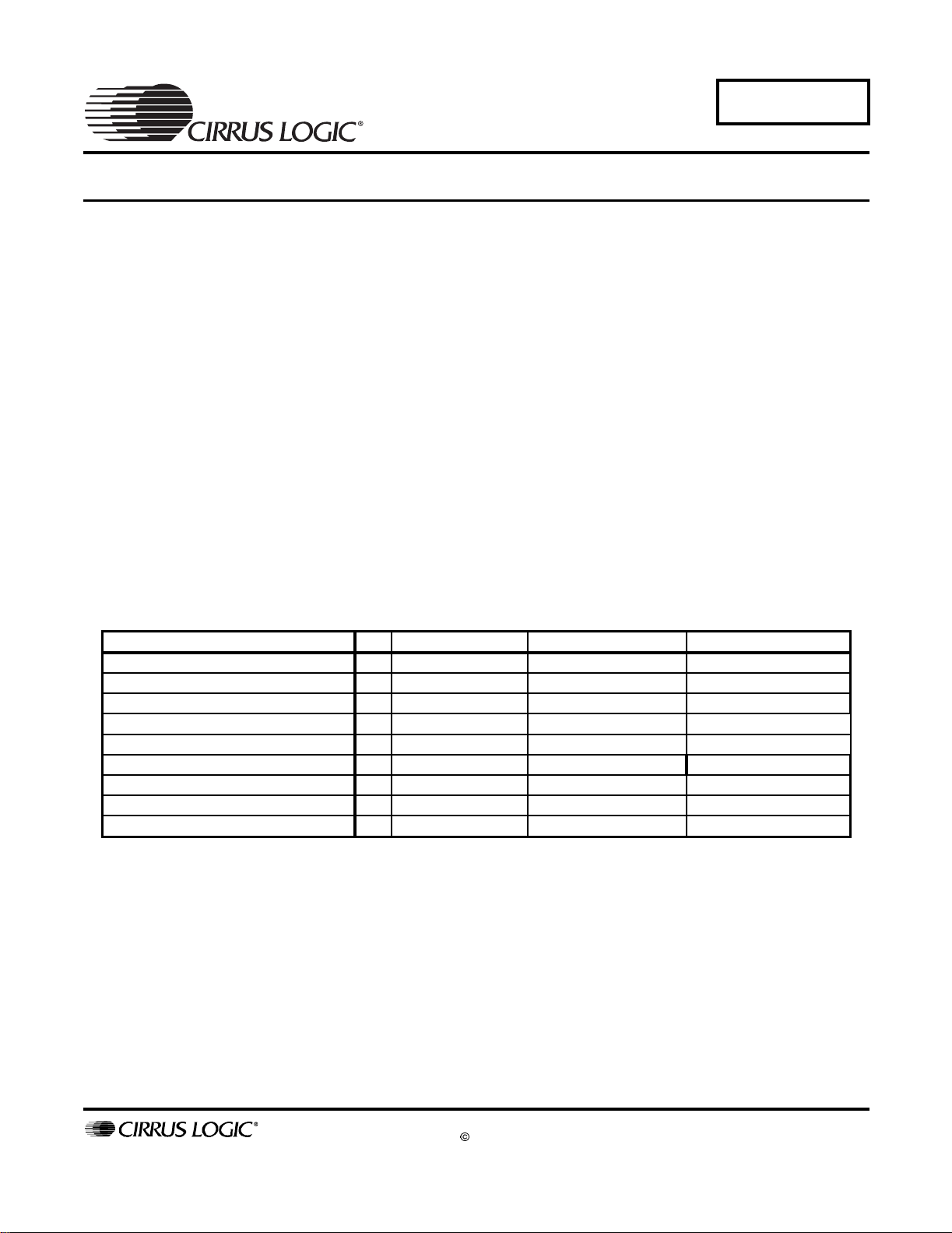
2. Typical Connection Diagrams
AN232
+5V
47µF
+
+5 V to 3.3 V
+
+
1µF
Analog
Input
Buffer
(Section 8)
Analog
Input
Buffer
(Section 8)
1µF
0.01µF
0.01µF
1µF
0.01µF
FILT+
REFGND
VQ
AINL+
AINL-
AINR+
AINR-
GND
+
VA V
*
Ω
5.1
D
CS5361
A/D CONVERTER
0.01 µF
L
V
0.01µF0.01µF
OVFL
2
I
S/LJ
HPF
MDIV
SDOUT
LRCK
SCLK
MCLK
GND
Figure 1. CS5361 Typical Connecti on Diagr am
RST
M/S
M0
M1
* Resistor may only be
used if VD is derived
from VA. If used , do
not drive any ot her
+
1µF
VL
10 kΩ
logic from VD
+5V to 2.5V
Power Down
and Mode
Settings
Audio Data
Processor
Timing Logic
andClock
200µ
+5 V to 3.3 V
+5V
+
F
1µF
+
Analog
Buffer
(Section 8)
Analog
Buffer
(Section 8)
+
1µF 0.1µF
+
1µF
0.1µF
0.1
FILT+
µ
F
*
Ω
5.1
VA V L
0.1
µF
µ
0.1
F
VD
REFGND
µ
F
Input
Input
0.1
VQ
AINL+
AINL-
AINR+
AINR-
GND
CS5381
A/D CONVERTER
OVFL
2
S/LJ
I
HPF
MDIV
SDOUT
LRCK
SCLK
MCLK
GND
RST
M/S
M0
M1
Figure 2. CS5381 Typical Connecti on Diagr am
+
1µF
VL
10 k
*
Resistor may only
be used if VD is
derived from VA. If
used, do not drive
any other log ic
from VD.
+5V to 2.5V
Power Down
and Mode
Settings
AudioData
Processor
Timing Logic
and Clock
2
Page 3
AN232
1
+5V
0µF
10µF
+
Analog
Input
Buffer
(Section 8)
Analog
Input
Buffer
(Section 8)
+
+
µ
10
0.1
0.22
0.22µF
µF 0.1
0.1
F
VA D
VREFL
µF
GNDL
µF
VCOML
AINL+
A/D CONVERTER
AINL-
AINR+
AINR-
VREFR
µF
0.1
GNDR
VCO MR
AGND
BGND
AK5393
TEST
V
ZCAL
HPFE
SMODE2
SMODE1
SDATA
LRCK
SCLK
MCLK
FSYNC
DGND
RST
CAL
DFS
10
µ
F
Reset and
Calibration
+5V to 3.3V
Control
Mode
Control
Audio Data
Processor
Timing Logic
and Clock
+
µF
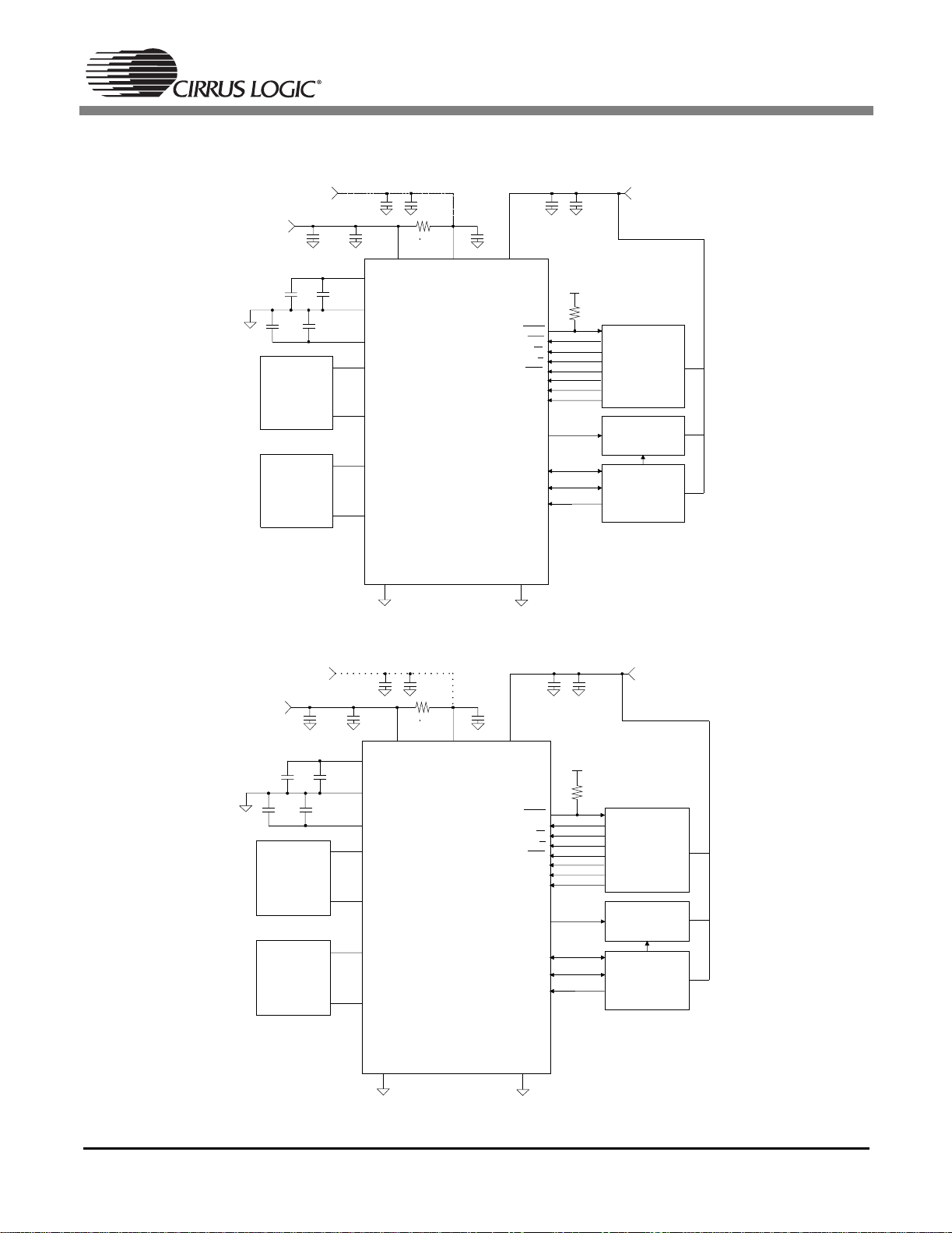
Figure 3. AK5393 Typical Connecti on Diagr am
3
Page 4

AN232
Pin Name
FILT+
Positive reference voltage
REFGND
Ground reference
VQ
Internal quiescent reference voltage
AINL+
Differential Left Channel Input
AINL-
Differential Left Channel Input
-
Zero Calibration Control
VD
Digital power
GND
Ground reference
-
Calibration Active Signal
RST
I2S/LJ
M/S
LRCK
Left right clock
SCLK
Serial clock
SDOUT
Serial data
-
Frame Synchronization Signal
MCLK
Master clock
M0
Mode Selection
HPF
-
Test
-
Substrate Ground
GND
Ground reference
VA
Analog power
AINR-
Differential Right Channel Input
AINR+
Differential Right Channel Input
M1
Mode Selection
VL
Logic Power
MDIV
MCLK divider
OVFL
3. Pin Compatibility
Table 2 sho ws t he pi ns of t he AK5 393 an d t he c or re sp ondi n g pi ns of the CS 5361 /8 1. Pl eas e no te th at th e
AK5393 has 28 pins, and the CS5361/81 has 24 pins.
AK5393 CS5361/81 Description
Pin Number Pin Name Pin Number
1, 28 VREFL, VREFR 24
2, 27 GNDL, GNDR 23
3, 26 VCOML, VCOMR 22
4 AINL+ 16
5 AINL- 17
6ZCAL 7VD 6
8DGND 7
9CAL -
10
11 SMODE2 12
RST
1
Reset
Serial Audio Interface Format Select
12 SMODE1 2
13 LRCK 3
14 SCLK 4
15 SDATA 9
16 FSYNC 17 MCLK 5
18 DFS 13
19 HPFE 11
20 TEST -
21 BGND 22 AGND 18
23 VA 19
24 AINR- 20
25 AINR+ 21
14
8
10
15
Table 2. Pin Compatibility Between AK5393 and CS5361/81
Master/Slave Mode Select
High Pass Filter Enable
Overflow
4. Offset Calibration
The CS5361, CS5381, and AK5393 all have offset calibration capability. However, the calibration process
varies slightly betwee n t he AK5393 and t he CS5361/CS5381.
4.1 CS5361 an d CS 5381
The CS5 361 and C S5381 im plem ent a hi gh pas s filte r that can be contro lle d via th e HPF
high pass filter continuously subtracts a measure of the DC offset from the output of the decimation filter.
If the HPF pin is tak en high during normal operation, th e current value of the D C offset reg is te r is frozen
and this DC of f se t wi ll co nt inue to be subtr ac t ed from the con v ers ion result.
4
pin (pi n 11). The
Page 5

AN232
A system calibration can then be performed by first running the CS5361 or CS5381 with the high pass
filter enable d (HPF = LO W) until t he filter se ttles. At th is point, d isable th e high pas s filter (HP F = HI),
thereby freezing the st ored DC offset.
4.2 AK5393
The AK5393 will autom at ic ally initiate a c alibration sequence following a reset. The CAL pin (pin 9) is an
output that indicates when a calibration sequence is in progress. This calibration technique is very similar
to that des cr ibed above fo r th e C S5361 and CS 5381.
The AK5393 also has a ZCAL pin (p in 6) whic h allows t he cal i brati on input t o be obtained from eith er the
analog input pins or the VCOM pins. The high pass filter can be controlled via the HPFE pin (pin 19). In
the AK5393, the high pass filter is either continuously running or completely removed from the signal path.
5. Master/Slave Selection and Digital Interface Format
The CS53 61, CS5381, and AK5393 are pin compatible in terms of sele c t ing Master/Sl av e operation and
digitial interface format. The pins match up as noted in Table 2.
6. Speed Mode Selection
The AK53 93 sup port s tw o sp eed m ode s, “norm al” a nd “doub le ” as dete rmin ed by th e DFS p in (pin 18 ).
This pin is c omp atibl e with t he M0 pin (pin 13) of the C S536 1 an d CS 5381, as sho wn in Tabl e 2. In this
case, the M1 pin (pin 14) of the CS5361 and CS5381 must be tied low.
7. System Clock ing
The CS 5361 an d CS 5381 ar e fu lly com pat ible wit h the clo cking re quirem ent s o f the AK 5393 . H owe ver,
there is a sligh t dif fere nce wh en o perat ing in M as ter m ode. If DFS = LOW , the AK 53 93 wil l gen erat e an
SCLK that is 128×Fs. The CS5361 and CS5381 generat e an SCLK that is 64×Fs.
The C S536 1 and C S53 8 1 of fe r a n i nt egr at ed M CLK di vi de r, whi ch ca n be co nt ro ll ed vi a th e MD I V pi n ( pi n
10). This pin all ows m ultip le ex tern al MCL K/LR CK ratio s to be supp orted . In ord er to m aint ain c om plete
compatibility between the AK5393 and the CS5361/CS5381, connect the MDIV pin (pin 10) of the
CS5361/CS5381 to GND.
8. Input Buffer Topology
The analog input buff ers shown in Figures 7 and 8 of the AK5393 data s heet (dated April, 2000) will also
work for the CS5361/81. In this case, the “Bias” reference should be sourced from the VQ pin of the
CS5361/81. However , t hese in put buffers require a la rge input voltage level at the inpu t t o t he buff er and
attenuate the signal p rior to the converter. Th is muc h signal swing is not always p ossible in a real system,
and not nec es s ary to achiev e t he full performa nc e of the CS5361 and CS538 1.
The follo win g se ctions co ntai n a d esc riptio n of a s ingle- en ded t o dif fere ntia l inpu t bu ffer (co mpa rable to
Figure 7 of the AK5393 da tashe et) and a fully diff erential input buf fer (com parable to Figure 8 of the
AK5393 datasheet). These two buffer topologies are unity gain, and therefore do not rely on a large input
voltage at the buffer input.
8.1 Single-Ended to Differential Input Buffer
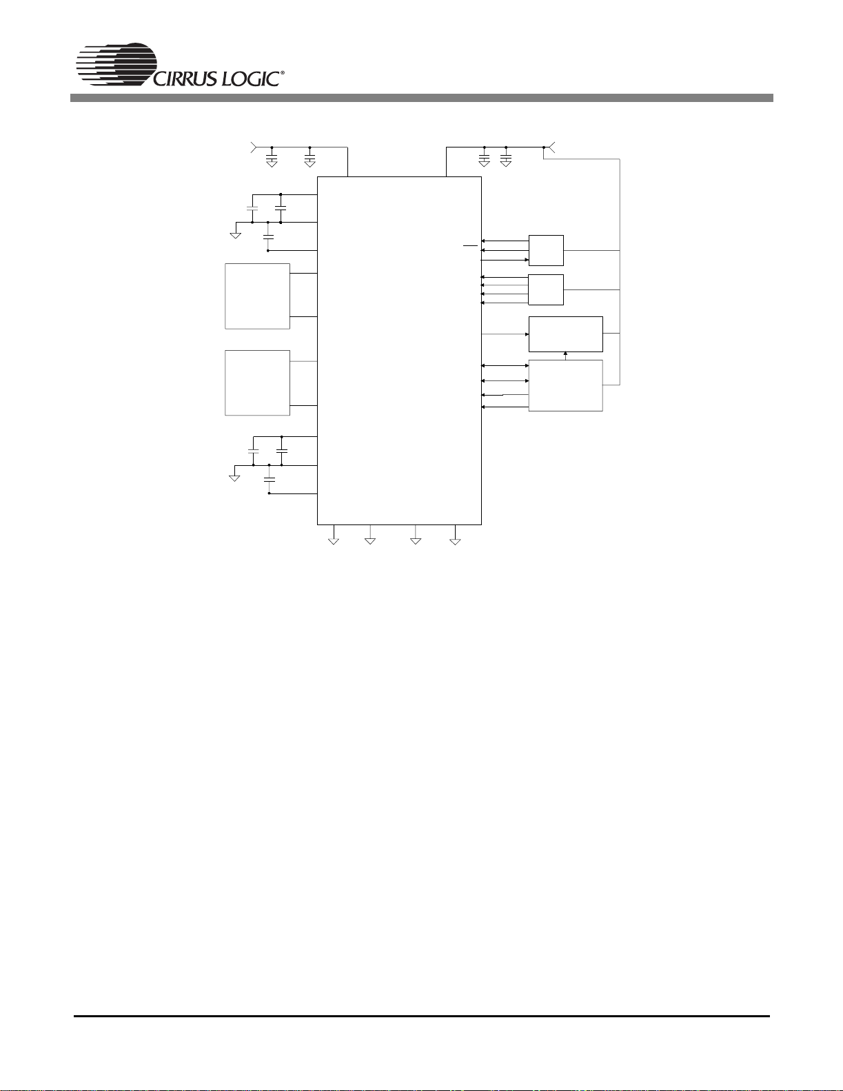
Figure 4 shows a single-ended to differential analog input buffer. This buffer provides the proper biasing,
isolation from the switched capacitor currents, low output impedance, and anti-alias filtering. The second
op-a m p s tage is s et up in an in v ertin g c onfiguration to produce t he negative node of t he diff erent ial in put.
In the inpu t buffer show n below, the second stag e has unity ga in, and the single-end ed input level will
effectively be doubled when presented differentially to the converter. For example, a 2.8 Vpp single-ended input will provide a full-scale 5.6 Vpp differential input to the CS5361/CS5381.
5
Page 6

100 kΩ
1
00 kΩ
3.3 kΩ
3.3 kΩ
3.3 kΩ
3.3 kΩ
1 µF
VA
1 µF
VA
470 pF
C0G
+
100 kΩ
0.01 µF 100 µF
470 pF
C0G
+
100 kΩ
0.01 µF100 µF
634 Ω
634 Ω
634 Ω
634 Ω
91 Ω
91 Ω
470 pF
+
470 pF
+
C0G
C0G
634 Ω
634 Ω
91 Ω
91 Ω
2700 pF
C0G
0.01 µF1 µF
2700 pF
C0G
AN232
CS5361/81
AIN+
AIN-
VQ
AIN+
AIN-
Figure 4. Single-Ended to Differential Input Buffer
8.2 Fully Differential Input Buffer
Figure 5 sh ows a fully diffe rential analo g input buf fer. This buffer provides the proper bia sing, isolation
from the swit ched capac itor currents, low output impe dance, an d anti-alias fil tering. This inpu t buffer is
unity gain, so a 5.6 Vpp differential input will provide a full-scale 5.6 Vpp differential input into the
CS5361/CS5381.
634 Ω
100 kΩ
100 kΩ
100 kΩ
100 kΩ
10 µF
10 kΩ
10 kΩ
10 µF
10 µF
10 kΩ
10 kΩ
10 µF
0.01 µF
0.01 µF
470 pF
C0G
+
-
+
-
+
-
+
470 pF
C0G
470 pF
C0G
470 pF
C0G
91 Ω
634 Ω
91 Ω
634 Ω
91 Ω
634 Ω
91 Ω
1 µF
2700 pF
C0G
0.01 µF
2700 pF
C0G
CS5361/81
AIN+
AIN-
VQ
AIN+
AIN-
Figure 5. Fully Differential Input Buffer
6
Page 7

AN232
t
,
r
r
l
-
-
-
,
Contacting Cirrus Logic Support
For all product questions and inquiries cont act a Cirrus Logic Sales Repr esentative.
To find one nearest you go to www.ci rrus.com/
IMPORTANT NOTICE
Cirrus Logic, Inc. and its subsidiaries ("Cirrus") believe that the information contained in this document is accurate and reliable. However, the information
is subject to change without notice and is provided "AS IS" without warranty of any kind (express or implied). Customers are advised to obtain the lates
version of rel evant information to verify, before placing orde rs, that informat i on being relied on is cu rrent and complete. All products are sold subject to
the terms and conditions of sale supplied at the time of order acknowledgment, including those pertaining to warranty, patent infringement, and limitation
of liability. No responsibility is assumed by Cirrus for the use of this information, including use of this information as the basis f or manufacture or sale
of any i tems, or f or i nfrin geme nt of p atent s or othe r r ight s of thir d p arties . T his do cu ment is t he prope rty of Ci rru s a nd by f urni shing thi s information
Cirrus g rants no l ice nse, expre ss or im plied und er any pa tents, mas k wo rk ri ghts , co pyri ghts , tr adem arks , tr ade se cret s or o th er in tellectual property
rights. Cirrus owns the copyrights associated with the information contained herein and gives consent for copies to be made of the information only fo
use within y our orga niz ati on with res pe ct to Ci rrus i ntegr ated circ uits or ot her pro duc ts of Ci rrus . This conse nt does not ext end to other copying such
as copying for general distribution, ad vertising or pr om otional purposes, or for creating any work for resale.
An export pe rm i t needs to be obtained fr om the competent authorities of the Ja panese Governm ent if any of the produc ts or technologies described in
this mat erial and c on troll ed un der the "For eign Exc ha nge an d Fo reig n Tr ad e Law" is to be ex port ed or ta ken o ut of Japa n. An expor t license and/o
quota needs to be obtained from the competent authorities of the Chinese Government if any of the products or technologies described in this materia
is subject to the PRC Foreign Trade Law and is to be exported or tak en out of the PRC.
CERTAIN APPLICATIONS USING SEMICONDUCTOR PRODUCTS MAY INVOLVE POTENTIAL RISKS OF DEATH, PERSONAL INJURY, OR SE
VERE PROPERTY OR ENVIRONMENTAL DAMAGE ("CRITICAL APPLICATIONS"). CIRRUS PRODUCTS ARE NOT DESIGNED, AUTHORIZED
OR WARRANTED FOR USE IN AIRCRAFT SYST EMS, MIL ITARY APPL ICATIONS, PR ODUCTS SU RGICALLY IMP LANTED I NTO THE BODY, LIFE
SUPPORT PRODUCTS O R OTH ER CRI T ICA L AP PLI CATI ONS ( IN CL UDING MED IC AL DEVICES, AIRCRAFT SYSTEMS OR COMPONENTS A ND
PERSONAL OR AUTOMOTIVE SAFETY OR SECURITY DEVICES). INCLUSION OF CIRRUS PRODUCTS IN SUCH APPLICATIONS IS UNDER
STOOD TO BE FULLY AT THE CUSTOMER'S RISK AND CIRRUS DISCLAIMS AND MAKES NO WARRANTY, EXPRESS, STATUTORY OR IM
PLIED, INCLU DI NG THE IMPLIED WARRANTI ES O F MERCHANTABILITY AN D FIT NES S FO R PA RTIC UL AR PUR POSE, WITH REGARD TO ANY
CIRRUS PRODUCT TH AT IS U SED IN SUC H A MANNER. IF TH E CU ST OMER O R CUS TOMER' S C USTOM ER USES OR PER MIT S TH E US E O F
CIRRUS PRODUCTS IN CRITICAL APPLICATIONS, CUSTOMER AGREES, BY SUCH USE, TO FULLY INDEMNIFY CIRRUS, ITS OFFICERS, DI
RECTORS, EMPLO YEES, DIST RIBUTORS A ND OTHER A GENTS FR OM ANY AND ALL LIABI LITY, I NCLUDING ATTORNEYS' FEES AND COSTS
THAT MAY RESULT FROM OR ARISE IN CONNECTION WITH THESE USES.
Cirrus Logic, Cirr us, and the Ci rrus Logic logo designs are tr ademarks of Cirrus L ogi c, Inc. Al l other brand and pro duct names in this document may
be tradema rks or service marks of their respective owner s.
7
 Loading...