

Page 1
AN229
Application Note
TRANSITIONING FROM THE CS8405A TO THE CS8406
by Sean Davis
1. Introduction
The CS8406 was designed as a pin and function compatible update for the CS8405A to add
192 kHz sample rate capability and offer over 1/3 less total power consumption than the
CS8405A. This document outlines the considerations that need to be accounted for when making the transition. Please refer to the latest revision of each part’s datasheet for a detailed
description of part operation.
2. Power Supply
The VD+ supply of the CS8405A operates only at 5.0 V ±10%, while the VD supply of the
CS8406 operates at either 3.3 V or 5.0 V ±5%. However, when the CS8406 is operated with
VD = 5.0 V, certain conditions apply:
V
In power down mode, it is recommended that all inputs be driven low to minimize current
(Min) for the CS8406 = 2.75 V. VIH (Min) for the CS8405A = 2.0 V.
IH
consumption.
3. Software Mode
Shown in Table 2 on page 2 is a list of pin numbers and their corresponding pin names for both
parts when operated in Software mode. The register settings for the CS8405A are compatible
with the CS8406.
4. Hardware Mode
Shown in Table 3 on page 3 is a list of pin numbers and their corresponding pin names for both
parts when operated in Hardware mode.
5. CS8406 Test Pins
The CS8406 has several pins labeled as TEST. These pins are unused inputs in either Software
or Hardware mode. It is recommended that these pins be tied to a supply (VL or GND) to minimize leakage current.
When transitioning from the CS8405A to the CS8406, some of the TEST pins on the CS8406
may be left floating due to corresponding pins on the CS8405A being labeled as no connects.
The CS8406 will operate the same if these pins are left floating, however current consumption
from VL will increase by 25 μA per pin that is left floating. As the CS8406 consumes much less
current than the CS8405A, this should not be a concern to the user.
http://www.cirrus.com
Copyright Cirrus Logic, Inc. 2009
(All Rights Reserved)
APRIL ‘09
AN229REV2
1
Page 2
AN229
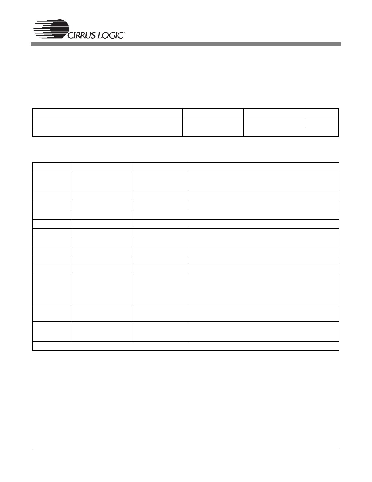
6. Output Resistance
The typical output resistance of the transmitter pins changed from the CS8405A to the CS8406.
The value of the external series resistor placed on the transmitter pins should be modified appropriately to account for this change. See the latest CS8406 datasheet for details on selecting the
value of the external resistor.
Parameter VL = 3.3 V VL = 5 V Unit
TXP/TXN CS8405A Output Resistance 40 26 Ω
TXP/TXN CS8406 Output Resistance 33.5 26.5 Ω
Table 1. Transmitter Output Resistance
Pin Number CS8405A Pin Name CS8406 Pin Name Differences
CS8405A I
1 SDA / CDOUT SDA / CDOUT
5 DGND2 TEST See “CS8406 Test Pins” on page 1.
6 VD+ VD See “Power Supply” on page 1.
7 DGND4 TEST See “CS8406 Test Pins” on page 1.
8 DGND3 TEST See “CS8406 Test Pins” on page 1.
10 NC1 TEST See “CS8406 Test Pins” on page 1.
11 NC2 TEST See “CS8406 Test Pins” on page 1.
16 NC3 TEST See “CS8406 Test Pins” on page 1.
17 NC4 TEST See “CS8406 Test Pins” on page 1.
18 NC5 TEST See “CS8406 Test Pins” on page 1.
21 OMCK OMCK
23 VL+ VL
28 SCL / CCLK SCL / CCLK
Pins 2, 3, 4, 9, 12, 13, 14, 15, 19, 20, 22, 24, 25, 26, and 27 have the same functions on both parts.
Table 2. Software Mode Comparison
CS8406 allows I
CS8405A OMCK clock ratios can be 256*Fs, 384*Fs,
or 512*Fs.
CS8406 OMCK clock ratios can be 128*Fs, 256*Fs,
384*Fs, or 512*Fs.
For both parts, the VL supply can operate at 3.3 V
or 5.0 V.
CS8405A I
CS8406 allows I
2CTM
is only supported at VL+ = 5.0 V.
2
C operation at VL = 3.3 V or 5.0 V.
2
C is only supported at VL+ = 5.0 V.
2
C operation at VL = 3.3 V or 5.0 V.
2
Page 3

AN229
Pin Number CS8405A Pin Name CS8406 Pin Name Differences
2 VL2+ TEST See “CS8406 Test Pins” on page 1.
6 VD+ VD See “Power Supply” on page 1.
7 DGND4 TEST See “CS8406 Test Pins” on page 1.
8 DGND3 TEST See “CS8406 Test Pins” on page 1.
Pins 20 and 27 set the OMCK clock ratio for the
CS8406. Setting both pins to VL (the recommended
setting from the CS8405A datasheet) or both pins to
GND will cause the clock ratio to be 256*Fs, the only
20 VL3+ HWCK0
21 OMCK OMCK
23 VL+ VL
27 VL4+ HWCK1
Pins 1, 3, 4, 5, 9, 10, 11, 12, 13, 14, 15, 16, 17, 18, 19, 22, 24, 25, 26, and 28 have the same functions on both parts.
Table 3. Hardware Mode Comparison
mode available for the CS8405A.
CS8405A OMCK clock ratio is 256*Fs.
CS8406 OMCK clock ratios can be 128*Fs, 256*Fs, or
512*Fs, set by HWCK[0:1].
For both parts, the VL supply can operate at 3.3 V
or 5.0 V.
Pins 20 and 27 set the OMCK clock ratio for the
CS8406. Setting both pins to VL (the recommended
setting from the CS8405A datasheet) or both pins to
GND will cause the clock ratio to be 256*Fs, the only
mode available for the CS8405A.
3
Page 4

7. Revision History
Contacting Cirrus Logic Support
For all product questions and inquiries contact a Cirrus Logic Sales Representative.
To find one nearest you go to
www.cirrus.com
IIMPORTANT NOTICE
Cirrus Logic, Inc. and its subsidiaries ("Cirrus" ) believ e that the i nformat ion contained in this docu ment is accur ate and rel iabl e. However, the informa-
tion is subject to change without notice and is provide d "AS IS" with out war ranty of any kind (e xpress o r implie d) . Cu stome rs a re advis ed to obtain th e
latest version of relevant information to verify, before placing orders, that information being relied on is current and complete. All products are sold subject to the terms and con dit io ns of sa le sup pl ied at the t ime of o rder a ckn owle dgme nt, i nclu di ng t h ose per taining t o war r anty, indemnification, and limitation of liability. No responsibility is assumed by Cirrus for the use of this in format ion , inclu ding use of thi s info rmatio n as t he b asi s for ma nufa ct ure or
sale of any items, or for infringement of patents or other rights of third parties. This document is the property of Cirrus and by furnishing this information,
Cirrus grants no license, express or implied under any patents, mask wo rk rights, copyrights, tradema rks, trade secrets or othe r intellectual property
rights. Cirrus owns the copyrights associated with the information contained herein and gives consent for copies to be made of the information only for
use within your organizatio n wi th resp ect t o Cir rus int egra ted c ircu it s or o th er pr oduc t s of C irrus . Th is co nsen t do es not extend to othe r co pyin g su ch as
copying for general distribu tion, advertising or promotional purposes, or for creating any work for resale.
CERTAIN APPLICATIONS USING SEMICONDUCTOR PRODUCTS MAY INVOLVE POTENTIAL RISKS OF DEATH, PERSONAL INJURY, OR
SEVERE PROPERTY OR ENVIRONMENTAL DAMAGE (“CRITICAL APPLICATIONS”). CIRRUS PRODUCTS ARE NOT DESIGNED, AUTHORIZED
OR WARRANTED FOR USE IN PRODUCTS SURGICALLY IMPLANTED INTO THE BODY, AUTOMOTIVE SAFETY OR SECURITY DEVICES, LIFE
SUPPORT PRODUCTS OR OTHER CRITICAL APPLICATIONS. INCLUSION OF CIRRUS PRODUCTS IN SUCH APPLICATIONS IS UNDERSTOOD
TO BE FULLY AT THE CUSTOMER’S RISK AND CIRRUS DISCLAIMS AND MAKES NO WARRANTY, EXPRESS, STATUTORY OR IMPLIED,
INCLUDING THE IMPLIED WARRANTIES OF MERCHANTABILITY AND FITNESS FOR PARTICULAR PURPOSE, WITH REGARD TO ANY CIRRUS PRODUCT THAT IS USED IN SUCH A MANNER. IF THE CUSTOMER OR CUSTOMER’S CUSTOMER USES OR PERMITS THE USE OF CIRRUS PRODUCTS IN CRITICAL APPLICATIONS, CUSTOMER AGREES, BY SUCH USE, TO FULLY INDEMNIFY CIRRUS, ITS OFFICERS,
DIRECTORS, EMPLOYEES, DISTRIBUTORS AND OTHER AGENTS FROM ANY AND ALL LIABILITY, INCLUDING ATTORNEYS’ FEES AND
COSTS, THAT MAY RESULT FROM OR ARISE IN CONNECTION WITH THESE USES.
Cirrus Logic, Cirrus, and the Cirrus Logic logo designs are trademarks of Cirrus Logic, Inc. All other brand and product names in this document may be
trademarks or service marks of th eir respective owners.
I2C is a trademark of Philips Semiconductor.
Revision Changes
REV1 Initial Release
REV2 Added “Output Resistance” on page 2
.
AN229
4
 Loading...