

Page 1
Application Note
CALIBRATING THE CS5460A
1. Is Calibration Required?
The CS5460A does not have to be calibrated. After
CS5460A is powered on and then reset, the device
is functional. This is called the active state.Upon
receiving a ‘Start Conversions’ command,
CS5460A can perform measurements without being calibrated. But the CS5460A’s output is always
affected by the values inside the various calibration registers. If no calibrations are executed by the
user, then these registers will contain the default
values (Gains = 1.0, DC Offsets = 0.0,
AC Offsets = 0). Although the CS5460A can be
used without performing an offset or gain calibration, the guaranteed ranges for accuracy of ±0.1%
of reading (with respect to a known voltage and
current level) will not be valid until a gain/offset calibration is performed. Although the CS5460A will
always exhibit the linearity+variation tolerances
that are specified in Table 1, the exact reference
AN227
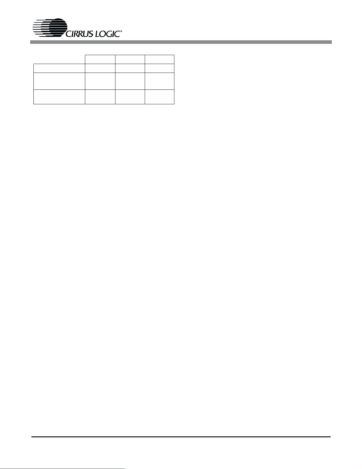
Before AC Gain Calibration (Vgain Register = 1)
250 mV
230 mV
DC Si gnal
INPUT
0V
SIGNAL
-250 mV
V
Register =
RMS
After AC Gain Calibration (Vgai n Regi ster changed to ~0.65217)
250 mV
230 mV
DC Si gnal
INPUT
0V
SIGNAL
-250 mV
V
RMS
230
/
=
250
Register = 0.6000...
0.92
Figure 2. Another Example of AC Gain Calibration
0.9999...
0.92
Instantaneous Voltage
Register Values
-1.0000...
0.65217
0.6000
Instantaneous Voltage
Register Values
-0.65217
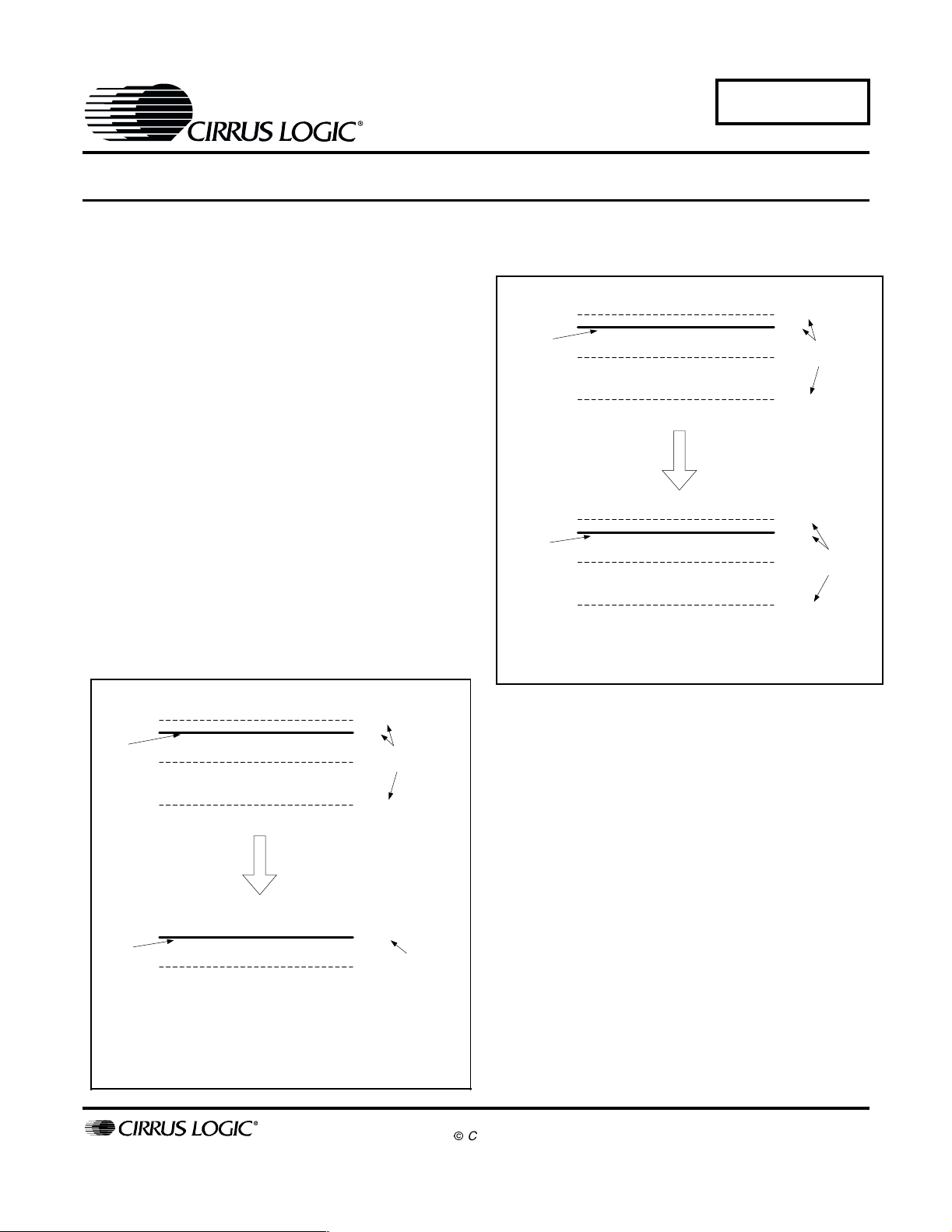
Before DC Gain Calibration (Vgain Register = 1)
250 mV
230 mV
DC Si gnal
INPUT
0V
SIGNAL
-250 mV
V
Register =
RMS
After DC Gain Calibration (Vgain Register changed to 1.0870)
230 mV
DC Si gnal
INPUT
0V
SIGNAL
V
RMS
230
/
=
250
Register = 0.9999...
0.92
Figure 1. Example of DC Gain Calibration
www.cirrus.com
0.9999...
0.92
Instantaneous Voltage
Register Values
-1.0000...
voltage and current levels to which this linearity is
referenced will vary from sample to sample. If no
calibration is performed, these voltage/current reference levels exist based on the full-scale DC input voltage limits for each channel, which are
approximately equal to the voltages specified in
the “Max Input” row of Table 1. But these voltages
will have a variation from part to part. Any given
CS5460A sample must be calibrated to insure the
guaranteed accuracy = (linearity+variation) abilities of the sample, with respect to a specific input
0.9999...
Instantaneous Voltage
Register Values
voltage signal levels at the voltage/current channel
inputs.
As an example, suppose the user runs the DC gain
calibration sequence on the current channel (assume PGA gain set for “10x”) using a calibration
signal level across the IIN+/IIN- pins of 187.5 mV
(DC). After this calibration is performed, the fullscale digital output code (0x7FFFFF in the Instan-
CopyrightCirrus Logic, Inc. 2003
(All Rights Reserved)
FEB ‘03
AN227REV1
1
Page 2
Energy Vrms Irms
Range (% of FS)
Max. Differential
Input
Linearity
Table 1. Available range of ±0.1% output linearity, with
default settings in the gain/offset registers.
0.1% - 100% 50% - 100% 0.2% - 100%
not applicable
0.1% of
reading
V-channel:
±250 mV
0.1% of
reading
I-channel:
±250 mV 10x
±50 mV 50x
0.1% of
reading
taneous Current Register) will be obtained whenever the input voltage across the IIN+ and IIN- pins
is 187.5 mV (DC). Note that this level is ~75% of
the (typical) maximum available input voltage
range [i.e, ~
±250 mV DC.] In this situation, the cur-
rent channel input ranges for which ±0.1% linearity
+ variation are guaranteed will be reduced to between 0.5 mV (DC) and 187.5 mV (DC), as opposed to what is specified in Table 1 [which would
translate into a voltage range between 0.5 mV
(DC) and 250 mV (DC)].
Also note that using gain calibration signal levels
which cause the CS5460A to set the internal gain
registers to a value that is less than unity will effectively decrease the guaranteed “±0.1% of reading”
linearity+variation range (and therefore the accuracy range) of the RMS calculation results and the
overall energy results. This will occur whenever a
DC gain calibration is performed (on either channel) of a CS5460A sample while applying a DC signal whose value is less than the individual
sample’s inherent maximum differential DC input
voltage level. This will also occur whenever an AC
gain calibration is performed (on either channel)
using an AC signal whose RMS value is less then
60% of the sample’s inherent maximum AC input
voltage levels.
Finally, remember that the ±0.1% (of reading) accuracy guarantee is made with the assumption that
the device has been calibrated with MCLK =
4.096 MHz, K = 1, and N = 4000. If MCLK/K becomes too small, or if N is set too low (or a combination of both), then the CS5460A may not exhibit
±0.1% linearity + variation.
1.1 Order of Calibration Sequences
Should offset calibrations be performed before
gain calibrations? Or vice-versa? This section
AN227
summarizes the recommended order of calibration.
1. If the user intends to measure any DC content
that may be present in the voltage/current and
power/energy signals, then the DC offset calibration sequences should be run (for both channels)
before any other calibration sequences. However if
the user intends to remove the DC content present
in either the voltage or current signals (by turning
on the voltage channel HPF option and/or the current channel HPF option--in the Status Register)
then DC offset calibration does not need to be executed for that channel. Note that if either the volt-
age HPF or current HPF options are turned on,
then any DC component that may be present in the
power/energy signals will be removed from the
CS5460A’s power/energy results.
2. If the user intends to set the energy registration
accuracy to within ±0.1% (with respect to reference
calibration levels on the voltage/current inputs)
then the user should next execute the gain calibrations for the voltage/current channels. The user
can execute either the AC or DC gain calibration
sequences (for each channel).
3. Finally, the user should (if desired) run the AC
offset calibration sequences for the voltage and
current channels. Simply ground the “+” and “-” inputs of both channels and execute the AC offset
calibration sequence.
Note that technically, by following the order of calibrations as suggested above, if DC offset calibration is performed for a given channel, and
afterwards a gain calibration is performed on the
channel, then the DC offset register value for the
channel should be scaled by a factor equal to the
respective channel’s new gain register value. For
example, suppose that execution of DC offset calibration for the voltage channel results in a value of
0x0001AC = 0.0000510(d) in the Voltage Channel
DC Offset Register (and we assume that the value
in the Voltage Channel Gain Register was at its default value of 1.000... during execution of this DC
offset calibration). Then if AC or DC gain calibration is executed for the voltage channel such that
the Voltage Channel Gain Register is changed to
0x4020A3(h) = 1.0019920(d), then the user may
want to modify the value in the Voltage Channel
2
Page 3

AN227
DC Offset Register to 0x0001AD(h) =
0.0000511(d), which is (approximately) equal to
1.0019920*0.0000510
.
1.2 Calibration Tips
To minimize digital noise, the user should wait for
each calibration step to be completed before reading or writing to the serial port.
After a calibration is performed, the offset and gain
register contents can be read and stored externally
by the system microcontroller and recorded in
memory. The same calibration words can be uploaded into the offset and gain registers of the converters when power is first applied to the system,
or when the gain range on the current channel is
changed.
Contacting Cirrus Logic Support
For all product questions and inquiries contact a Cirrus Logic Sales Representative.
To find one nearest you go to www.cirrus.com
IMPORTANT NOTICE
“Preliminary” product information describes products that are in pr oduction, but for which full characteri zation data i s not yet available. “Advance” product information describes products that are in devel opment and subject to development changes. Cirrus Logic, Inc. and its subsidiaries (“Cirrus”) beli eve that the information contained in this document is accurate and reliable. However, the information is subject to change without notice and is provided “AS IS” without warranty
of any kind (express or implied). Customers are advised to obtain the latest version of relevant information to verify, before placi ng orders, that information being
relied on is current and complete. All products are sold subject to the t erms and conditions of sale supplied at the time of order acknowledgment, including those
pertaini ng to warranty, patent infringement, and limitation of liabil ity. No responsibi lity is assumed by Cirrus for the use of thi s informati on, i ncluding use of this
informati on as the basis for manufacture or sale of any items, or for i nfringement of patents or other rights of third parties. Thi s document is the property of Cirrus
and by furnishing this information, Cirrus grants no license, express or implied under any patents, mask work rights, copyrights, trademarks, trade secrets or
other intellectual property rights. Cirrus owns the copyrights associated wi th the informati on contai ned herei n and gi ves consent for copies to be made of the
informati on only for use within your organi zation with respect to Cirrus integrated circuits or other parts of Cir rus. This consent does not extend t o other copying
such as copying for general distri bution, advertisi ng or promotional purposes, or for creating any work for resale.
An export permit needs to be obtained from the competent authorities of the Japanese Government if any of the products or technologies described in thismaterial and controlled under the “ Foreign Exchange and Foreign Trade Law” is to be exported or taken out of Japan. An export license and/or quota needs to be
obtained from the competent authorit ies of the Chinese Government if any of the products or technologies described in this material is subject to the PRC Foreign
Trade Law and is to be exported or taken out of the PRC.
CERTAIN APPLICATIONS USING SEMICONDUCTOR PRODUCTS MAY INVOLVE POTENTIAL RISKS OF DEATH, PERSONAL INJURY, OR SEVERE
PROPERTY OR ENVIRONMENTAL DAMAGE (“CRITICAL APPLICATIONS”). CI RRUS PRODUCTS ARE NOT DESIGNED, AUTHORIZED, OR WARRANTED TO BE SUITABLE FOR USE IN LIFE-SUPPORT DEVICES OR SYSTEMS OR OTHER CRITICAL APPLICATIONS. INCLUSION OF CIRRUS PRODUCTS
IN SUCH APPLICATIONS IS UNDERSTOOD TO BE FULLY AT THE CUSTOMER'S RISK.
Cirrus Logic, Cirrus, and the Cirrus Logic logo designs are trademarks of Cirrus Logic, Inc. All other brand and product names in this document may be trademarks or service marks of their respective owners. Microwire is a trademark of National Semiconductor Corporati on.
3
Page 4

 Loading...