Page 1

AN165
Application Note
CS4297A/CS4299 EMI REDUCTION TECHNIQUES
1. INTRODUCTION
The CS4297A and CS4299 AC ’97 audio codecs
are based on a new and faster fabrication process,
and certain precautions in the analog I/O circuitry
may be required to prevent 49.1 MHz commonmode radiation. Note that 49.1 MHz is 2 times the
CS4297A internal clock frequency of 24.576 MHz.
2. DESCRIPTION
Common-mode radiation is the result of undesired
voltage drops due to voltage differentials in the I/O
ground system. The CS4297A clock transitions result in a rush of current that may induce the digital
ground plane to "bounce". When external speaker
or microphone cables are connected to the audio
system, any common-mode voltage potential on
the analog ground will drive the cables (antennas)
and radiate electric fields. The magnitude of the
electric fields are th e result of the I/O ca ble length
(the antenna) and the magnitude of common-mode
current.
3. EMI SHUNTING CIRCUIT
The key to reducing common-mode emissions is to
add decoupling (called shunting) at the audio I/O
connectors. The shunt capacitors must be connected to a "clean" (free of digital noise) I/O ground.
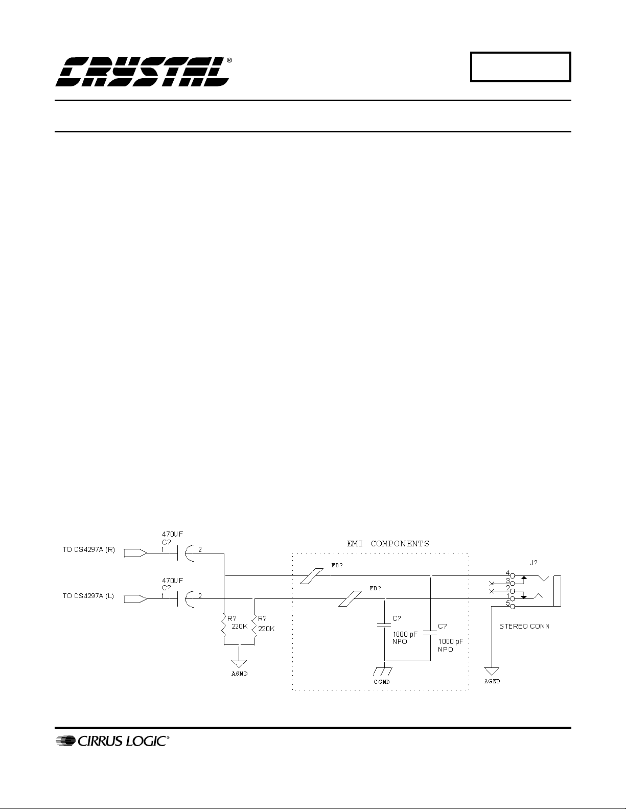
The recommended EMI shunting circuit is shown
in the following diagram, and includes ferrite beads
and 1000 pF NPO capacitors. The ferrite bead values are typically selected for an impedance of
100 ohms at 100 MHz. The ferrite bead and capacitor circuit create a low pass filter to attenuate frequencies above 1.6 MHz.
Additionally, the following PCB layout checklist
includes generally accepted practices for reducing
both differential-mode and common-mode radiated
emissions, while maintaining audio quality.
P.O. Box 17847, Austin, Texas 78760
(512) 445 7222 FAX: (512) 445 7581
http://www.cirrus.com
Copyright Cirrus Logic, Inc. 2000
(All Rights Reserved)
MAY ‘00
AN165REV1
1
Page 2

AN165
4. PCB LAYOUT CHECKLIST
• Connect analog and digital ground together
with a 1/16 inch trace under the CS4297A. A
direct connection between analog and digital
ground will reduce the differential-mode radiation and improve the EOS (Electrical Overstress) capabilities of the CS4297A.
• Construct a "clean" chassis ground on the PCB
around the I/O connectors, and connect the I/O
ground to the system frame ground.
• Connect chassis ground to digital ground in a
quiet area, away from the CS4297A.
• The ferrite bead and decoupling capacitor combination shown in the block diagram on page
one of this document, form a low-pass filter to
remove the common-mode voltages. The de-
coupling capacitor must be terminated to a
clean (free of digital noise) I/O chassis ground.
A separate analog ground return path between
the I/O connectors and analog ground plane
must be maintained to reduce loop areas.
• Chassis and analog planes should be identical
on all layers, and the gap or "moat" between
planes should be 1/8 inch to prevent coupling
between planes. The absolute minimum moat
spacing is 1/16 inch. Do not overlap digital and
analog ground planes.
• Never route digital traces or digital planes under the analog or I/O chassis ground areas. Analog components should be located over analog
planes and digital components should be located over digital planes.
Contacting Cirrus Logic Support
For a complete listing of Direct Sales, Distributor, and Sales Representative contacts, visit the Cirrus Logic web site at:
http://www.cirrus.com/corporate/contacts/
Preliminary product inf o rmation describes products whi ch are in production, b ut f or wh i ch f ull characterization data i s not yet available. Advance pr odu ct i nfor mation describes products which are in development and subject to development changes. Cirrus Logic, Inc. has made best efforts to ensure that the information
contained in this document i s accurat e and reli able. However , t he infor mation is subje ct to chang e without noti ce and is provi d ed “AS IS” without warrant y of
any kind (express or implied). No responsibility is assumed by Cirrus Logic, Inc. for the use of this information, nor for infringements of patents or other rights
of third parties. This document is the pro perty of Cirrus Logi c, Inc. and i mplie s no licen se under patents, copyrights, tr ademarks, or trade secre ts. No part of
this publication may be copied, reproduced , stored in a retrieval system, or transmitted, in any form or by any means (electro nic, mechanical, photographic, or
otherwise) without the pr i or writ ten consent of Cirrus Logic, Inc. It e ms f rom any Ci rrus L ogi c websi t e or disk may be printed for use by the user. However, no
part of the printout or electronic files may be copied, reproduced, stored in a retrieval system, or transmitted, in any form or by any means (electronic, mechanical,
photographic, or otherwise) without the prior written consent of Cirrus Logic, Inc.Furthermore, no part of this publication may be used as a basis for manufacture
or sale of any items without the prior written consent of Cirrus Logic, Inc. The names of products of Cirrus Logic, Inc. or other vendors and suppliers appearing
in this document may be trademarks or service marks of their respective owners which may be registered in some jurisdictions. A list of Cirrus Logic, Inc. trademarks and service marks can be found at http://www.cirrus.com.
2 AN165REV1
Page 3

• Notes •
Page 4

 Loading...