Page 1

AN158
Application Note
MEASURING HIGH VOLTAGES (5 TO 1,000 VOLTS) WITH
THE CS5521/23, CS5522/24/28, AND CS5525/26 A/D
CONVERTERS
By
Keith Coffey & Jerome Johnston
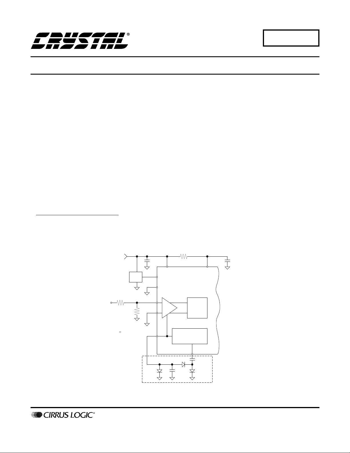
The CS5521/23, CS5522/24/28, and CS5525/26
A/D converters include a low input current (<300
pA input current over -40 to +85°C), chopper-stabilized programmable gain instrumentation amplifier (PGIA). A charge pump control loop is also
included on-chip to provide a negative supply to
the amplifier. This pump, which uses external com-
1.The CS5529 is not included in this Application
Note because it does not contain an instrumentation
amplifier.
VIN
+5 V
Voltage
Divider
2.5 V
0.1 µF
VA+
VREF+
VREF-
+
PGIA
-
1
ponents, enables the amplifier to measure groundreferenced signals even though the A/D is powered
from a single +5 V supply (see Figure 1).
This applications note discusses the features of the
amplifier and how it can be used to measure large
dc voltages.
INPUT CVF (SAMPLING) CURRENT
The programmable gain instrumentation amplifier
in the CS552x family is a CMOS, chopper-stabi-
Ω
10
0.1 µF
VD+
∆Σ
ADC
P.O. Box 17847, Austin, Texas 78760
(512) 445 7222 FAX: (512) 445 7581
http://www.cirrus.com
PGIA set for
+
100 mV
V
≈
-2.1 V
NBV
Charge Pump
Regulator
1N4148
10
µ
F
+
CPD
1N4148BAT85
0.033
µ
F
Figure 1. CS552X ADC with Charge Pump
Copyright Cirrus Logic, Inc. 1999
(All Rights Reserved)
Charge Pump
Circuitry
AUG ‘99
AN158REV1
1
Page 2

AN158
lized amplifier with has three low level input rang-
es (±25 mV, ±55 mV, and ±100 mV) and very low
input current. The amplifier’s input current is dynamic current (CVF current; for explanation of
CVF current, see the Summary) which is caused by
charge injection. Charge injection occurs due to inherent mismatch of the chopping switches in the
chopper circuitry of the amplifier.
The magnitude of the CVF current is a function of
the frequency used to operate the chopping switches. The CS552x family has two bits in the configuration register (Chop Frequency Select bits) which
allow the user to program the rate of the chopping
frequency, (i.e. the user can control the magnitude
of the input CVF current). When set for the lowest
chopping rate, the chop clock frequency is 256 Hz
when XIN = 32.768 kHz. Note that if the XIN clock
frequency is changed, the chop frequency scales
proportionally. At a chop clock rate of 256 Hz, the
CVF current of the PGIA inputs will be below
300 pA over the industrial temperature range. For
the 100 mV input range at 25 °C, this equates to an
input impedance of approximately 1000 MΩ
(100 mV/ 100 pA).
Many competitors ADCs, which are “designed” for
low level signal measurement, exhibit CVF input
currents of 10-30 nA, or as much as 100 times higher. This current is typically not specified in the
datasheet.
will not exceed 300 pA over the industrial temperature range if XIN = 32.768 kHz and the lowest
chop clock frequency (256 Hz) is used. The ratio of
these two currents is about 3333 to 1; therefore the
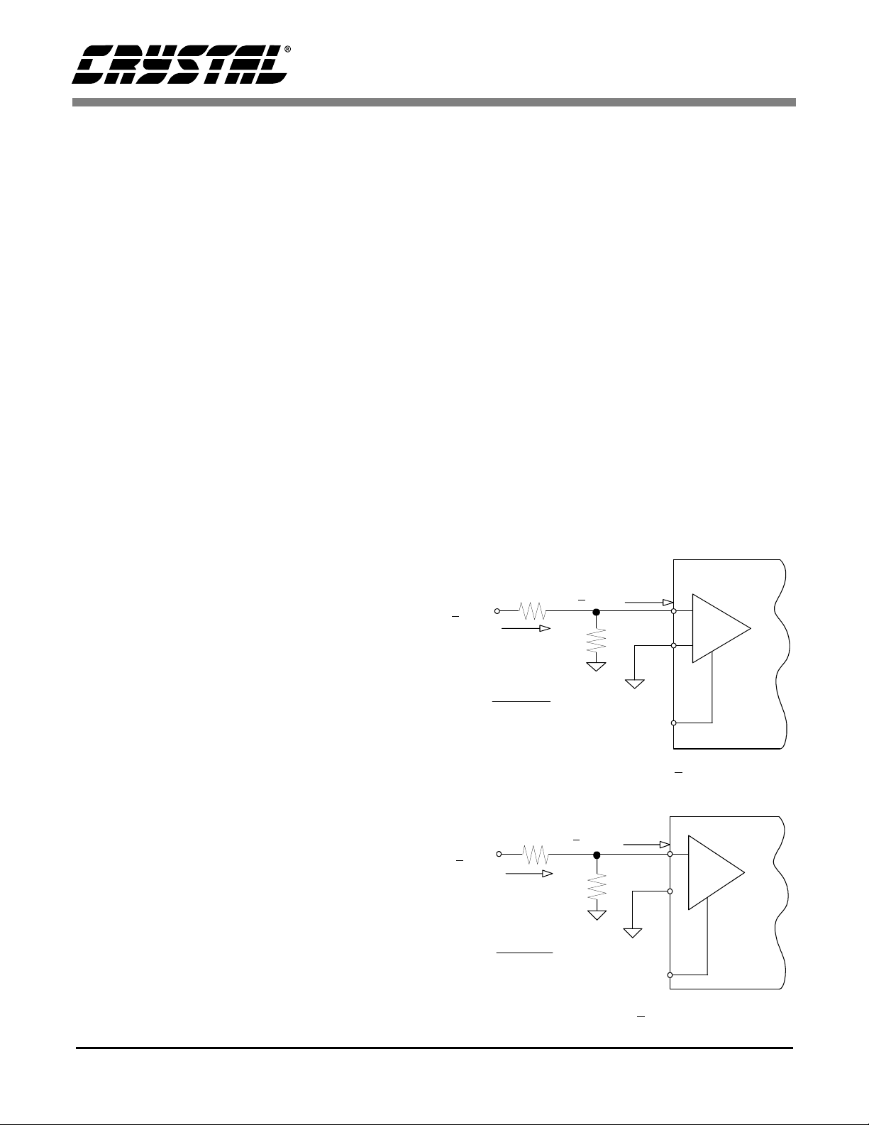
possible measurement error, due to the CVF current, is approximately 1/3333 or about 0.03%. Figure 3 illustrates an alternative divider with less
initial error due to the CVF current, typically
0.003%. Note that errors caused by initial resistor
tolerances and by the initial CVF current can be removed by using system calibration (refer to the
CS552x datasheet for more detail on system calibration). Since these initial errors can be removed,
the residual error becomes a function of the resistor
tempco and the drift of the CVF current. Figure 4
illustrates an example of the measurement of a very
high voltage: 1,000 V dc. If very high voltages are
measured be certain the resistors have adequate
voltage breakdown capability and sufficient power
dissipation capability.
10 M
Ω
+ 300 pA max
10 V
+
≈
1 µA F.S.
300 pA
1
PGIA set for ± 100 mV
= 0.03%
µ
A
100 k
Ω
-2.1 V
+
PGIA
-
NBV
MEASURING HIGH VOLTAGES
Figure 2. Resistor Divider for + 10 V Input
The very low CVF current on the ±100 mV and
lower ranges allows the use of fairly large source
impedances in front of the amplifier. This enables
this series of ADCs to use high impedance resistive
dividers in front of the ADC to divide down high
10 V
+
1 M
≈
10 µA F.S.
Ω
+ 300 pA max
10 k
Ω
+
PGIA
-
level input voltages.
Figure 3 illustrates an example of the ADC being
used with external divider resistors to achieve the
measurement of a ±10 V input signal. The input
current from the 10 V source will be about 10 µA
(10 V/ 10MΩ). The input current to the amplifier
2 AN158REV1
300 pA
10
PGIA set for ± 100 mV
Figure 3. Alternate +
µ
A
= 0.003%
-2.1 V
NBV
10 V Divider
Page 3

+ 1000 V
2 M
AN158
Ω
2 M
Ω
+ 100 µA
2 M
2 M
2 M
Ω
Ω
Ω
+ 300 pA max
1 K
+
PGIA
-
300 pA
100
µ
PGIA set for ± 100 mV
Figure 4. Resistive Divider for Very High Voltage
SUMMARY
CVF current is a sampling current caused by a capacitive-based sampler. A sample capacitor is
charged with a voltage when a sample is taken. The
CVF current which flows is determined by the
equation I= CVF, where C is the value of the sampling capacitor, V is the voltage magnitude being
sampled with the capacitor, and F is the sampling
frequency. An ADC with low input CVF current
will exhibit a high input impedance. A high input
impedance allows for a high source impedance
= 0.0003 %
A
-2.1 V
NBV
from the signal to be converted. In this applications
note example, high voltages can be measured using
a simple high resistance ratio voltage divider.
Refer to Applications Note 30, “Switched-Capacitor A/D Converter Input Structures”, as it further
discusses the magnitude of CVF currents for different switched-capacitor input structures. Also, refer
to Applications Note 152, “Using the CS552x’s
Charge Pump Drive for External Loads”, for more
details on using the CS552x’s charge pump to drive
external loads.
AN158REV1 3
Page 4

 Loading...