

Page 1
AN152
Application Note
USING THE CS5521/23, CS5522/24/28, AND CS552 5/26
CHARGE PUMP DRIVE FOR EXTERNAL LOADS
By Bill Durbin and Jerome Johnston
INTRODUCTION
The CS5521/23, CS5522/24/28, and CS5525/26
series of A/D converters include on-chip circuitry
to drive and regulate a diode charge pump. The
purpose of this application note is to explain the
charge pump circuitry and how it can be used in a
system design.
CS552X Overview
The CS5521/23, CS5522/24/28, and CS5525/26
series of A/D converters include a chopper-stabilized instrumentation am plifier for measureme nt of
low level dc signals (±100 mV or less). This amplifier is designed to produce very low input sampling
1.The CS5529 is not included in this Application
Note because it does not contain a charge pump.
Ve
+
-
T/C
10 K
10 K
0.1 uF
current (I
input current minimizes the errors that can occur in
1
< 300 pA over -40 to +85 C). A low
CVF
thermocouple measurements when high impedance
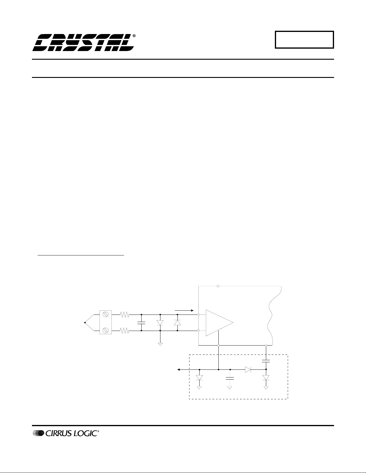
circuitry is used for input protection as shown in
Figure 1.
The charge pump circuitry, illustrated in Figure 1,
is used to generate a negative supply (approximately -2.1 V) to power the on-chip instrumentation
amplifier. This enables the amplifier to measure
low level input signals that are negative relative to
ground while maintaining low input current. Within certain constraints, which are described in this
document, the charge pump can be used to power
some additional circuitry outside the converter,
such as an amplifier or a multiplexer.
VA+
CS5521/23,
CS5522/24/28,
I
+
-
& CS5525/26
P.O. Box 17847, Austin, Texas 78760
(512) 445 7222 FAX: (512) 445 7581
http://www.cirrus.com
NBV
External Load
BAT85
+
Charge Pump Circuit
Figure 1. Input Amplifier inside CS552x ADCs.
Copyright Cirrus Logic, Inc. 1999
(All Rights Reserved)
CPD
1N4148
1N4148
AUG ‘99
AN152REV1
1
Page 2
Frequency = f
+5 V
Q
AN152
1
C
1
D
2
-V
Q
Figure 2. Charge Pump Components
V
D
C
1
-
+
D
I
1
(a) (b)
Figure 3. Charge Pump Cycle Sequence
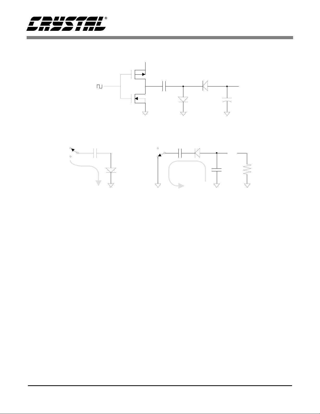
Charge Pump Basics
Figure 2 illustrates a basic diode charge pump.
Transistors Q1 and Q2 represent the output transistors of a CMOS inverter. When the input to the inverter causes transistor Q1 to be turned on (Q2 is
off) C1 is charged through diode D1 to a voltage of
approximately 5 V minus the forward voltage of
the diode. When the output of inverter switches to
Q1 off, Q2 on, the positively charged lead of C1
will be connected to ground. Since the voltage
across a capacitor cannot change instantaneously,
the lead of C1 which is connected to diode D2 will
go negative, turning on diode D2. The charge on
C1 will then flow onto C2 and produce a negative
output voltage. Capacitor C2 acts as a reservoir for
charge and is much larger than the charge pump capacitor C1. After many charge pump cycles, capacitor C2 will be charged to a voltage that is about
two diode drops below 5 V.
Figure 3 illustrates each of the two charge pump se-
2
D
1
C
2
+
C
+
D
1
-
2
V
0
I
C
2
+
R
L
quences. Capacitor C2 acts as a reservoir for
charge and is much larger than the charge pump capacitor C1.
The CS552X’s Charge Pump
Figure 4 illustrates a simplified version of t he basic
charge pump regulation loop that is inside the A/D
converters listed in this application note. The
charge pump drive pin (CPD) is driven from a
clock (CPCLK) derived from the XIN frequency.
In the CS5525 and CS5526 the XIN frequency is
used directly. The CS5521/22/23/24/28 devices
use a clock that is XIN/2. A regulator loop compares the magnitude of the voltage generated on the
charge reservoir capacitor to a proportion of the
VA+ supply magnitude. The loop is designed to
regulate the voltage at NBV to be -[VA+/2.38] V.
Note that if the VA+ supply voltage to the chip is
above +5 V, the voltage that results out of the
charge pump on NBV will be proportionally more
negative. When the voltage on the NBV pin reach-
2 AN152REV1
Page 3

AN152
VA+ = 5 V
+
-
-1x
Load Current
Extra
Load
RD C
NBV
L3
D , D = 1N4148
2
1
D = BAT 85
3
Figure 4. ADC Charge Pump Regulation Loop
es the proper magnitude, cycles of the charge pump
clock are deleted. The regulation loop maintains
the pulse rate out of the CPD pin at an average frequency that yields the proper output voltage. The
CPD driver output is supplied from the VD+ supply
as shown in Figure 4. This can be +5 V or +3 V.
The diode charge pump shown in Figure 4 is for a
+5 V supply. Diode D3, a Schottky, ensures that the
NBV pin will not go more than a diode drop above
ground. This ensures proper start-up of the regulator loop. Figure 5 illustrates the diode connections
needed if VD+ is 3 V.
Figure 6 illustrates a plot of the average freque ncy
VD+ = 5 V
CPCLK
D
DGND
1
CPD
C
1
+
-
Partial of ADC
D
2
2
+
output from CPD when the external load on the
output of the charge pump is changed. The charge
pump clock (CPCLK) is derived from XIN/2,
therefore the maximum frequency which can be
output from CPD is equal to XIN/2.
The load current in each of the plots exclude the
current used by the on-chip instrumentation amplifier (approximately 450 µA for the CS5525/26; 375
µA for the CS5521/23; and 700 µA for the
CS5522/24/28).
The plot illustrates the average CPD frequency for
two different sizes of charge pump capacitors with
the VA+ supply adjusted to 4.5, 5.0 and 5.5 V. The
Figure 5. Charge Pump Drive Diode Circuit For VD+ = 3V
AN152REV1 3
Page 4

1600
1400
1200
AN152
1000
(µA)
800
Load Cu rrent (uA)
600
400
200
0
0.00 2.00 4.00 6.00 8.00 10.00 12.00 14.00 16.00 18.00
Figure 6. Load Current vs. Frequency for the CS5521/23 and CS5522/24/28; VA+ = VD+
plot shows that if the charge pump output has no
external load, its average output frequency (VA+ =
5 V, C =0.033 uF) is approximately 8 kHz which is
about ½ the maximum possible output frequency.
The charge pump runs at this average frequency to
support the load of the on-chip instrumentation amplifier.
Figure 7 illustrates load current vs. CPD frequency
for the CS5525/26 devices. The charge pump clock
(CPCLK) is derived from XIN (set to 32.768 kHz),
therefore the maximum frequency which can be
output from CPD is equal to XIN.
The plots show data similar to tha t in figure 6. Because the charge pump frequency in the CS5525/26
devices is twice as fast as that used in the
CS5521/22/23/24/28 devices, the charge pump capacitor is ½ the size (for the same X IN clock frequency).
V
5
.
5
6
0
.
0
Frequency (KHz)
@
F
u
8
u
8
6
0
.
0
V
0
.
5
@
F
u
8
6
0
.
0
V
5
.
4
@
F
u
3
3
0
.
0
3
0
.
0
0
.
0
V
5
.
5
@
F
F
u
3
3
3
V
0
.
5
@
5
.
4
@
F
u
Figure 8 illustrates the CS5521/22/23/24/28 with
the charge pump capacitor increased to 0.15 µF.
This charge pump capacitor is about 4.5 times larger than the nominal capacitor. Under this condition
the charge pump could readily supply 2 mA to an
external load. While the pl ot indicates that 3 mA
can be supplied, it is not recommended that the external load exceed 2 mA. This allows for some
margin in the design. The actual maximum output
load capability is affected by the tolerances of
VA+, VD+, and the tolerance limits of the charge
pump capacitor.
Figures 9 and 10 illustrate the CS5521/22/23/24/28
running with a VD+ supply of 3 V. Figure 9 indicates the variation in load current capa bility when
VA+ varies from 4.5 to 5.5 V (VD+ =3.0 V). Figure 10 illustrates the variation in load capability
when VA+ is a constant 5.0 V, but VD+ is varied
V
4 AN152REV1
Page 5

(µA)
Load Current (uA)
1400
1200
1000
800
600
400
200
AN152
V
5
.
5
@
F
u
3
3
0
.
0
3
3
0
.
0
V
0
.
5
@
F
u
u
3
3
0
.
0
V
5
.
4
@
F
u
5
1
0
.
0
0
V
5
.
5
@
F
u
5
1
0
.
1
0
.
0
V
0
.
5
@
F
u
5
V
5
.
4
@
F
(µA)
Load Current
0
0.0 5.0 10.0 15.0 20.0 25.0 30.0 35.0
Frequency (KHz)
Figure 7. Load Current vs. Frequency for the CS5525/26; VA+ = VD+
3500
3000
2500
2000
1500
1000
500
0
0.00 2.00 4.00 6.00 8.00 10.00 12.00 14.00 16.00 18.00
Frequency
Figure 8. Load Current vs. Frequency; VA+ = VD+ = 5 V, Capacitor Size = 0.15 uF; CS5521/22/23/24/28
AN152REV1 5
Page 6

1000
900
800
700
(µA)
600
500
Load Current
400
300
200
100
0
0.0 2.0 4.0 6.0 8.0 10.0 12.0 14.0 16.0 18.0
+
A
V
Frequency
V
5
.
4
=
V
0
.
5
=
+
A
V
V
5
.
5
=
+
A
V
Figure 9. Load Current vs. Frequency for VD+ = 3.0 V, Capacitor Sizes = 0.47 uF
CS5521/22/23/24/28
AN152
1200
1000
800
V
3
.
3
(µA)
600
Load Current (uA )
400
200
0
0.0 2.0 4.0 6.0 8.0 10.0 12.0 14.0 16.0 18.0
=
+
D
V
V
Frequency (KHz)
V
0
.
3
=
+
D
7
.
2
=
+
D
V
Figure 10. Load Current vs. Frequency for VA+ = 5.0 V, Capacitor Sizes = 0.47 uF
CS5521/22/23/24/28
6 AN152REV1
Page 7

AN152
from +3.3 down to 2.7 V. The external load capability of the charge pump is limited when VD+ gets
to 2.7 V.
quency is changed to some other frequency, the
charge pump capacitor should be scaled inversely.
For example, if XIN is scaled from 32.768 kHz to
100 kHz, the charge pump capacitor should re-
Running the CS552X at Frequencies other than 32.768 kHz
The XIN frequency into the converters is used to
derive the charge pump clock frequency. The XIN
duced to about 1/3 of the value used at 32.768 kHz.
See the appendix for more exact equations which
can help determine the value of the charge pump
capacitor.
frequency is nominally 32.768 kHz. If this fre-
APPENDIX
Equation for charge pump as depicted in figure 4.
I = vfc
Current = Voltage x Frequency x Capacitor
I
+ I
NBV
I
= Current via NBV pin. Nominally 450µA for CS5525/26; 375 µA for CS5521/23; and 700 µA for
NBV
CS5522/24/28.
= [(VD+) - (2 x VD) - (2.1 V)] [η CPCLK] [CC]
EXT
I
= Current via External Load
EXT
VD+ = VD+ supply Voltage; typically 5 V.
VD = Forward Diode Voltage; typically 0.65 V.
-2.1 V = Regulated value of NBV (could use VA+/2.38 if VA+ is other than 5.0 V).
CPCLK = Charge Pump Clock. Nominally 32.768 kHz for CS5525 and CS5526; 16.384 kHz for
CS5521/22/23/24/28.
η = Duty cycle of CPCLK (average CPCLK frequency / maximum CPCLK frequency) to regulate NBV,
typically 0.3 to 0.7.
Choose CC to give the proper I
NBV
+ I
with the lowest VD+ and η set to some value between 0.3 and
EXT
0.7.
Note: I
should never exceed 2 mA.
EXT
AN152REV1 7
Page 8

 Loading...