

Page 1
AN131
Application Note
Interfacing the CS5521/22/23/24/28 to the 68HC05
TABLE OF CONTENTS
1. INTRODUCTION ................................................... 1
2. ADC DIGITAL INTERFACE ................................... 1
3. SOFTWARE DESCRIPTION ................................. 2
3.1 Initialize ............................................................. 2
3.2 Write Channel Setup Registers ........................ 2
3.3 Self-Offset Calibration ....................................... 3
3.4 Read/Write Gain Register ................................. 3
3.5 Acquiring Conversions ...................................... 4
4. MAXIMUM SCLK RATE ......................................... 4
5. CONCLUSION ....................................................... 5
6. APPENDIX: 68HC05 MICROCODE TO INTERFACE
TO THE CS5521/22/23/24/28 ................................ 6
1. INTRODUCTION
This application note details the int erface of Ci rrus
Logic’s Crystal® CS5521/22/23/24/28 Analog-to-
Digital Converter (ADC) to a Motorola 68HC05
microcontroller. This note takes the reader through
a simple example describing how to communicate
with the ADC. All algorithms discussed are i ncluded in Section 6. “APPENDIX: 68HC05 Microcode
to Interface to the CS5521/22/23/24/28” on page 6.
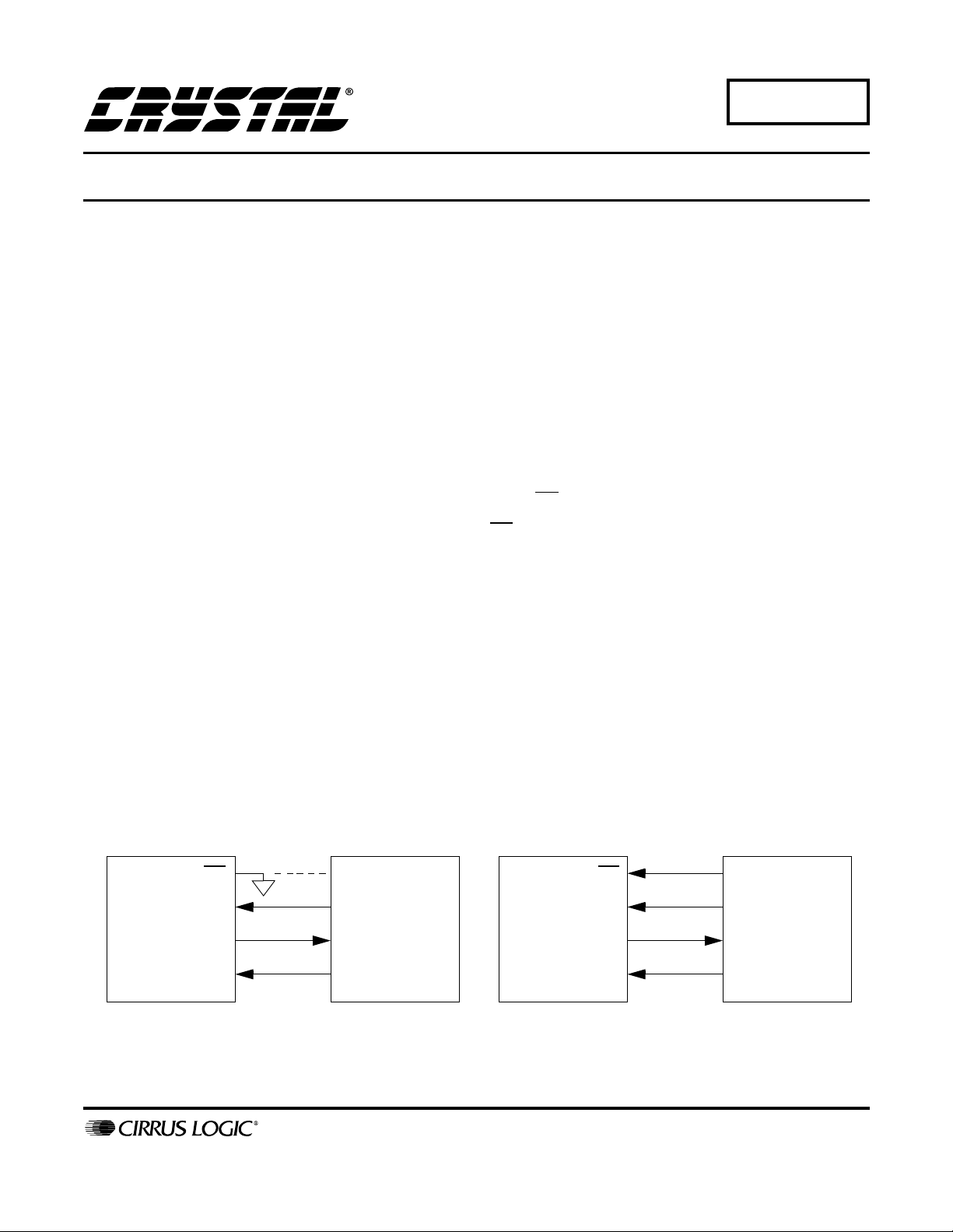
2. ADC DIGITAL INTERFACE
The CS5521/22/23/24/28 interfaces to the 68HC05
through either a three-wire or a four-wire interface.
Figure 1 depicts the interface between the two devices. Though this software was written to interface to the three-wire SPITM on the 68HC05, the
algorithms can be easily modified to work in the
four-wire format.
The ADC’s serial port consists of four control
lines: CS, SCLK, SDI, and SDO.
CS, Chip Select, is the control line which enables
access to the serial port.
SCLK, Serial Clock, is the bit-clock which controls
the shifting of data to or from the ADC’s serial
port.
SDI, Serial Data In, is the data signal used to transfer data from the 68HC05 to the ADC.
SDO, Serial Data Out, is the data signal used to
transfer output data from the ADC to the 68HC05.
3-Wire Interface 4-Wire Interface
CS5521/22/23/24/28 68HC05
CS
SDI
SDO
SCLK
P.O. Box 17847, Austin, Texas 78760
(512) 445 7222 FAX: (512) 445 7581
http://www.cirrus.com
No Connect
MOSI (PD3)
MISO (PD2)
SCK (PD4)
Figure 1. 3-Wire and 4-Wire Interfaces
CS5521/22/23/24/28
CS
SDI
SDO
SCLK
Copyright Cirrus Logic, Inc. 1999
(All Rights Reserved)
68HC05
PA0
MOSI (PD3)
MISO (PD2)
SCK (PD4)
NOV ‘99
AN131REV2
1
Page 2
AN131
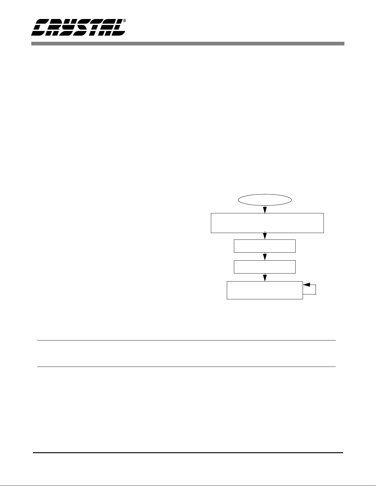
3. SOFTWARE DESCRIPTION
This note presents algorithms to initialize the
68HC05 and the CS5521/22/23/24/28, modify the
CS5521/22/23/24/28’s internal registers, perform
calibrations, and acquire conversions. Figure 2 depicts a block diagram of the program structure.
While reading this application note, please refer to
Section 6. “APPENDIX: 68HC05 Microcode to Interface to the CS5521/22/23/24/28” on page 6 for
the code listing.
3.1 Initialize
Initialize is a subroutine that configures the SPI on
the 68HC05 and places the CS5521/22/23/24/28
into the command state. The SPI is configured as
depicted in Figure 1 by selecting the 68HC05 as the
master. To function properly with the
CS5521/22/23/24/28, the SPI must be set up to use
a clock which idles low, and begins clocking data
with a rising edge in the center of the first bit (for
more information on configuring the SPI refer to
Motorola’s 68HC05 Application Guide). After
configuring the SPI, the controller enters a delay
state to allow time for the CS5521/22/23/24/28’s
power-on-reset and oscillator to start-up (oscillator
start-up time for a 32.768 KHz crystal is typically
500 ms). The last step is to reinitialize the serial
port on the ADC (reinitializing the seri al port is unnecessary here, and the code is for demonstration
purposes only). This is implemented by sending the
converter fifteen bytes of logic 1’s followed by one
final byte, with its LSB at logic 0. This sequence
places the serial port of the ADC into the command
state, where it waits for a valid command.
3.2 Write Channel Setup Registers
The subroutine write_csrs is an example of how to
write to the CS5521/22/23/24/28’s Channel Setup
Registers (CSRs). For this example, two CSRs
(four Setups) are written. The number of CSRs to
be accessed is determined by the Depth Pointer bits
(DP3-DP0) in the configuration register. The
Depth Pointer bits are set to “0011” to access the
two CSRs. The value “0011” is calculated by tak-
START
INITIALIZE MICROCONTROLLER
AND CS55 21/22/23/24/28
SELF-OFFSET CAL.
MODIFY GAIN
ACQUIRE CONVERSION
Figure 2. CS5521/22/23/24/28 Software Flowchart
Contacting Cirrus Logic Support
For a complete listing of Direct Sales, Distributor, and Sales Representative contacts, visit the Cirrus Logic web site at:
http://www.cirrus.com/corporate/contacts/
SPI™ is a trademark of Motorola.
Microwire™ is a trademark of National Semiconductor.
Preliminary product inf o rmation describes products whi ch are in production, but for which full characteriza t i on da t a i s not yet available. Advance produ ct i nfor-
mation describes products which are in development and subject to development changes. Cirrus Logic, Inc. has made best efforts to ensure that the information
contained in this document i s accurat e and reli able. However , t he infor mation is subje ct to chang e without noti ce and is provi de d “AS IS” without warranty of
any kind (express or implied). No responsibility is assumed by Cirrus Logic, Inc. for the use of this information, nor for infringements of patents or other rights
of third parties. This document is the pro perty of Cirrus Logi c, Inc. and i mplie s no licen se under patents, copyrights, tr ademarks, or trade secre ts. No part of
this publication may be copied, reproduced , stored in a retrieval system, or transmitted, in any form or by any means (electronic, mechanical, photographic, or
otherwise) without the pr i or writ ten consent of Cirrus Logic, Inc. Ite ms f rom any Ci rrus L ogi c websi t e or disk may be printed for use by the user. However, no
part of the printout or electronic files may be copied, reproduced, stored in a retrieval system, or transmitted, in any form or by any means (electronic, mechanical,
photographic, or otherwise) without the prior written consent of Cirrus Logic, Inc.Furthermore, no part of this publication may be used as a basis for manufacture
or sale of any items without the prior written consent of Cirrus Logic, Inc. The names of products of Cirrus Logic, Inc. or other vendors and suppliers appearing
in this document may be trademarks or service marks of their respective owners which may be registered in some jurisdictions. A list of Cirrus Logic, Inc. trademarks and service marks can be found at http://www.cirrus.com.
2 AN131REV2
Page 3

AN131
ing the number of Setups to be accessed and subtracting 1. Because each CSR holds two Setups,
this number must always be an odd value, that is,
DP0 must always be logic 1 when reading and writing the CSRs. To modify the Depth Pointer bits, the
configuration register is read to prevent corruption
of other bits. After the read_register routine is run
with the command 0x0B (HEX), the DP3-DP0 bits
are masked to “0011”. Then, the updated information is written back into the ADC with the command 0x03 (HEX) using the write_register routine.
After the depth pointer bits are set correctly, the
CSR information is written to the ADC. The command 0x05 (HEX) is sent to the ADC to begin the
write sequence (to read the CSRs, the command
would be 0x0D). At this point, the ADC is expecting to receive information for two 24-bit CSRs, or
48 bits, based on the Depth Pointer bits. The first
CSR is written with a value of 0x000000 (HEX).
This sets Setup 1 and Setup 2 both to convert bipolar, 100mV signals on physical channel 1 (PC1) at
an output word rate (OWR) of 15 Hz, and latch pins
A1-A0 equal to “00”. The second CSR is written
with the value 0x4C0105 (HEX). This sets Setup 3
to convert a bipolar, 100mV signal on PC2 at a
101.1 Hz OWR, with latch pins A1-A0 at “01”.
This also sets Setup 4 to convert a unipolar, 25mV
input signal at 15 Hz on PC3, with out put latch pins
A1-A0 set to “00”.
3.3 Self-Offset Calibration
Calibrate is a subroutine that performs a self-offset
calibration using Setup 1. Calibrate does this by
sending the command 0x81 (HEX) to the ADC
through the SPI. This tells the ADC to perform a
self-offset calibration using Setup 1 (see the
CS5522/24/28 and CS5521/23 Data Sheets for information on performing offset or gain calibrations
using other Setups). Once the command has been
sent, the controller polls MISO (SDO) until it falls,
indicating that the calibration is complete. Note
that although calibrations are done using a specific
Setup, the offset or gain register that is modified
belongs to the physical channel referenced by that
Setup.
3.4 Read/Write Gain Register
The routine rwgain provides an example of how to
modify the ADC’s internal gain registers. To modify the gain register the command byte and data
byte variables are written with the appropriate information. rwgain then calls the subroutine
write_register, which uses these variables to set the
contents of Physical Channel 1 (PC1)’s gain register to 0x800000 (HEX). The write_register routine
calls the send_spi algorithm four times, once to
send the command byte, and three more times to
send the three data bytes. Send_spi is a subroutine
which transfers data to the CS5521/22/23/24/28
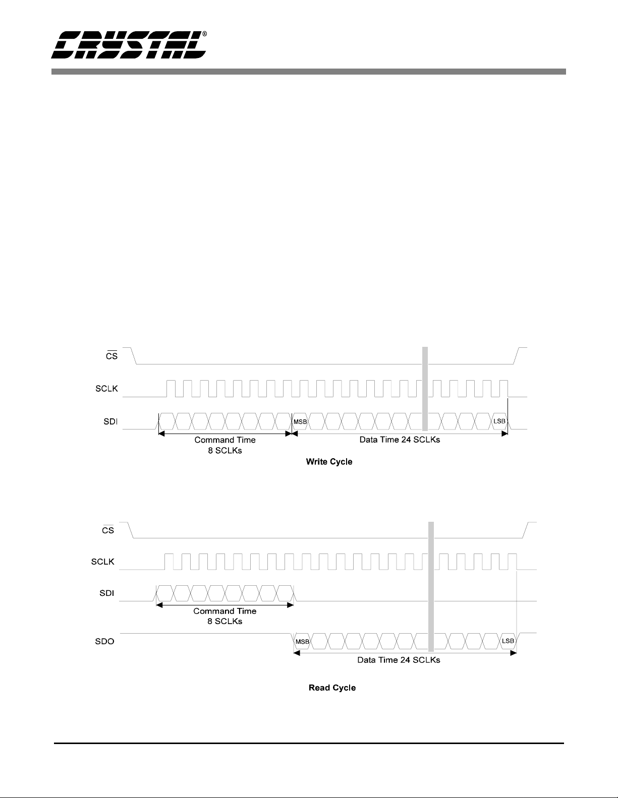
MSB-first through the SPI. Figure 3 depicts the
timing diagram for the write-cycle in the
CS5521/22/23/24/28’s serial port. It is important to
note here that this section of the code demonstrates
how to write to the gain register of PC1. It does not
perform a gain calibration. To write to the other internal registers of the ADC, follow the procedures
outlined in the CS5522/24/28 and CS5521/23 data
sheets.
To read the value in the gain register of PC1, the
command byte is loaded with the value 0x0A
(HEX), and the read_register routine is called. It
duplicates the read-cycle timing diagram depicted
in Figure 4. Read_register calls send_spi once to
transfer the command-byte to the
CS5521/22/23/24/28. This places the converter
into the data state where it waits until data is read
from its serial port. Read_register then calls
receive_spi three times and transfers three bytes of
information from the CS5521/22/23/24/28 to the
68HC05. Similar to send_spi, receive_spi acquires
a byte one bit at a time, MSB-first from the SPI.
When the transfer is complete, the variables
high_byte, mid_byte, and low_byte contain the value present in PC1’s 24-bit gain register.
AN131REV2 3
Page 4
AN131
3.5 Acquiring Conversions
To acquire a conversion the subroutine convert is
called. For single conversions on one physical
channel, the MC (multiple conversion) and the LP
(loop) bits in the configuration register must be logic 0. To prevent corruption of the configuration
register, convert instructs the 68HC05 to read and
save the contents. This information is stored in the
variables HIGHBYTE, MIDBYTE and LOWBYTE. Then the MC, LP, and RC (read conver t)
bits are masked to logic 0, and the new information
is written back to the ADC’s co nfiguration regis ter.
A conversion is initiated using Setup 1 by sending
the command 0x80 to the converter. At this time,
the controller polls MOSI (SDO) until it falls to a
logic 0 level (see Figure 5). After SDO falls, con-
vert calls send_spi to send one byte of all 0’s to the
converter to clear the SDO flag. The 68HC05 then
reads the conversion data word by calling
receive_spi three times. Figure 6 depicts how the
16 and 24-bit data words are stored in the memory
locations HIGHBYTE, MIDBYTE, and LOWBYTE.
4. MAXIMUM SCLK RATE
A machine cycle in the 68HC05 consists of 2 oscillator periods or 500 ns if the microcontroller’s oscillator frequency is 4 MHz. Since the
CS5521/22/23/24/28’s maximum SCLK rate is
2 MHz, additional no operation (NOP) delays may
be necessary to reduce the tra nsfer rate if the microcontroller system requires higher rate oscillators.
Figure 3. Write-Cycle Timing
Figure 4. Read-Cycle Timing
4 AN131REV2
Page 5
SCLK
SDI
*
t
ommand Time
C
8SCLKs
DO
S
td = XIN/OWR clock cycles for each conversion except the
*
first conversion which will take XIN/OWR + 7 clock cycles
d
Data SDO Continuous Conversion Read
Figure 5. Conversion/Acquisition Cycle Timing
SCLKs Clear SDO Flag
8
5. CONCLUSION
AN131
IN/OWR
X
Clock Cycles
SB
M
ata Time
D
24 SCLKs
SB
L
MSB High-Byte
D23 D22 D21 D20 D19 D18 D17 D16
Mid-Byte
D15 D14 D13 D12 D11 D10 D9 D8
Low-Byte
D7 D6 D5 D4 D3 D2 D1 D0
A) 24-Bit Conversion Data Word (CS5522/24/28)
MSB High-Byte
D15 D14 D13 D12 D11 D10 D9 D8
Mid-Byte
D7 D6 D5 D4 D3 D2 D1 D0
Low-Byte
1110CI1CI0ODOF
B) 16-Bit Conversion Data Word (CS5521/23)
0- always zero, 1- always one,
CI1, CI0 - Channel Indicator Bits
OD - Oscillation Detect, OF - Overflow
Figure 6. Bit Representation/Storage in 68HC05
This application note presents an example of how
to interface the CS5521/22/23/24/28 to the
68HC05. It is divided into two main sections: hardware and software. The hardware interface illustrates both three-wire and a four-wire interface.
The three-wire interface is SPI and Microwire™
compatible. The software section illustrate s how to
initialize the converter and microcontroller, write
to the CSRs, write and read the ADC’s interna l registers, perform calibrations, and acquire conversions. The software is modularized and provides
important subroutines such as write_register,
read_register, write_csrs and convert, which were
all written in 68HC05 assembly language.
The software described in the note is included in
Section 6. “APPENDIX: 68HC05 Microcode to Interface to the CS5521/22/23/24/28” on page 6.
AN131REV2 5
Page 6

AN131
6. APPENDIX: 68HC05 MICROCODE TO INTERFACE TO THE CS5521/22/23/24/28
;*****************************************************************************
;* File: 55226805.ASM
;* Date: September 23, 1998
;* Revision:0
;* Processor:68HC05
;*
;* Program entry point at routine ’main’. Entry point address is $100
;*
;* This program is an example on how to interface a 68HC05 Microcontro ller
;* to a CS5521/22/23/24/28 ADC. The program interfaces via the SPI port (Port D)
;* on the microcontroller, which controls the serial communications,
;* calibration, and conversion cycles.
;*****************************************************************************
;*** Memory Map Equates ***
PORTA EQU $00 ;General Purpose I/O Port
DDRA EQU $04 ;Data Direction Control for Port A
PORTD EQU $03 ;Port D Direct Pin Access (Input)
SPCR EQU $0A ;Serial Peripheral Control Register
SPSR EQU $0B ;Serial Periph e ral S tatus Register
SPDR EQU $0C ;Serial Peripheral Data I/O Register
SPIF EQU 7 ;Serial Peripheral Data Transfer Flag
;*** RAM Values ***
ORG $50
HIGHBYTE RMB 1 ;Upper 8 bits of Conversion Register
MIDBYTE RMB 1 ;Middle 8 bits of Conversion Register
LOWBYTE RMB 1 ;Lower 8 bits of Conversion Register
COMMAND RMB 1 ;Command Byte storage location
;*****************************************************************************
;* Program Code
;************* *** *** ********************************* *** *** *******************
ORG $100
;************* *** *** ********************************* *** *** *******************
;* Routine - main
;* Input - none
;* Output - none
;* This is the entry point and the main loop of the program.
;*****************************************************************************
6 AN131REV2
Page 7

MAIN EQU * ;Start from reset vector
;*** Initialize and Calibrate the system ***
JSR initialize ;Initialize the System
JSR write_csrs ;Modify the Chann e l Setup Registers
JSR calibrate ;Calib rate ADC Offset
JSR rwgain ;Write and read gain register
;*** Continuously perform single conversions ***
mloop: JSR convert ;Obtain a conversion from the ADC
JMP mloop ;Keep Looping
;*** End MAIN ***
;*****************************************************************************
;* Subroutines
;************* ********************************** ***************** *************
AN131
;************* ********************************** ***************** *************
;* Routine - initialize
;* Input - none
;* Output - none
;* This subroutine initializes Port D as a SPI port to interface to the
;* CS5521/22/23/24 / 28 ADC .
;* A time delay for the ADC oscillator start-up period is provided, as well
;* as a delay for the ADC’s power-on reset.
;* Typically, a 32.768 KHz crystal has a start-up time of about 500ms. After
;* this delay, an additional 1003 XIN cycles are delayed for the ADC reset.
;* The ADC’s serial port is also reset at this time
;*****************************************************************************
initialize LDA #%01010000 ;Load ACCA with values for SPCR
STA SPCR ;Setup SPI Port
LDA #$40 ;Load ACCA with delay count value
JSR delay ;Delay 1003 XIN for power-on reset
LDA #220 ;Load ACCA with delay count value
JSR delay ;Delay for oscillator start-up 170ms
JSR delay ;Delay for oscillator start-up 170ms
JSR delay ;Delay for oscillator start-up 170ms
;*** Initialize ADC serial port ***
LDX #$0F ;Value of 15 for first 15 Bytes
LDA #$FF ;Load ACCA with all 1’s
sloop: JSR send_sp i ;Send info to ADC
DECX ;Decrement Counter
AN131REV2 7
Page 8

BNE sloop ;Repeat loop if counter isn’t zero
LDA #%11111110 ;Load ACCA with last byte
JSR send_spi ;Send final byte to ADC
RTS ;Exit routine
;*****************************************************************************
;* Routine - write_csrs
;* Input - none
;* Output - none
;* This subroutine is used to write to the Channel Setup Reg isters. It first
;* changes the depth pointer bits in the configuration register to reflect
;* the number of CSRs to be written, and then writes information to th e
;* appropriate number of CSRs.
;*****************************************************************************
write_csrs LDA #$0B ;Command to read config. register
STA COMMAND ;Prepare command byte
JSR read_register;Read the configuration register
;*** Mask DP3-DP0 to access two CSRS (four Setups) ***
LDA MIDBYTE ;Get Middle Byte in ACCA
AND #$3F ;Mask DP3-DP2 low
ORA #$30 ;Mask DP1-DP0 high
STA MIDBYTE ;Put info back in to Middle Byte location
LDA #$03 ;Command to write back to config Register
STA COMMAND ;Prepare Command Byte
JSR write_register;Write Configuratio n Register
AN131
;*** Write to CSRs - note, the ADC expects information for the number of
; CSRs indicated in the Depth Bits (DP3-DP0 in the configuration
; register) so all of the CSRs must be written at this time.
LDA #$05 ;Command to write CSRs
JSR send_spi ;send command to ADC
;*** Setup CSR #1 - Setups 1 and 2
; Sets both Setups to a default value of ’000’
; (A1-A0 = 00, Physical Channel = 1, OWR = 15Hz,
; Input V-range = 100mV, Bipolar Measurement Mode)
LDA #$00 ;Load ACCA with zeros
JSR send_spi ;One byte of zero...
JSR send_spi ;Two bytes of zero...
JSR send_spi ;Three bytes of zero.
;*** Setup CSR #2 - Setups 3 and 4
; Sets Setup 3 to ’4C0’ and Setup 4 to ’105’
; Setup 3 Settings - (A1-A0 = 01, Physical Channel = 2, OWR = 101.1Hz,
; input V-range = 100mV, Bipolar)
8 AN131REV2
Page 9

; Setup 4 Settings - (A1-A0 = 00, Physical Channel = 3, OWR = 15Hz,
; input V-range = 25mV, Unipolar)
LDA #$4C ;Load ACCA with first byte of CSR #2
JSR send_spi ;Send byte number one
LDA #$01 ;Load ACCA with second byte of CSR #2
JSR send_spi ;Send byte number two
LDA #$05 ;Load ACCA with third byte of CSR #2
JSR send_spi ;Send byte number three
RTS ;Exit subroutine
;*****************************************************************************
;* Routine - calibrate
;* Input - none
;* Output - none
;* This subroutine instructs the CS5521/22/23/24/28 to perform a self-calibration on
;* Setup 1.
;************* ***************** ***********************************************
AN131
calibrate LDA #$81 ;Command for Self-Offset Cal, Set up 1
JSR send_spi ;Send Self-Cal command to ADC
poll_sdo1 BRSET 2,PORTD, poll_sdo1 ;Wait for SDO to fall
RTS ;Exit Routine
;*****************************************************************************
;* Routine - rwgain
;* Input - none
;* Output - cont ents of gain registe r on PC1 in HIGH, MID and LOW bytes
;* This subroutine first writes, and then reads back the value of the gain
;* register on Physical Channel 1
;*****************************************************************************
;*** Write to Gain Register of Physical Channel 1 ***
rwgain LDA #$02 ;Command to Write Gain Register of PC 1
STA COMMAND ;Prepeare COMMAND byte
LDA #$80 ;Value for High Byte
STA HIGHBYTE ;Prepare HIGHBYTE
CLR MIDBYTE ;Prepare MIDBYTE
CLR LOWBYTE ;Prepare LOWBYTE
JSR write_register;Write to Gain Register
;*** Read From Gain Register of Physical Channel 1 ***
LDA #$0A ;Command to Read Gain Register of PC 1
STA COMMAND ;Prepare COMMAND byte
JSR read_register;Read from Gain Register
RTS ;Return
AN131REV2 9
Page 10

AN131
;*****************************************************************************
;* Routine - convert
;* Input - none
;* Output - conversion results in memory locations HIGHBYTE, MIDBYTE and
;* LOWBYTE. This algorithm performs single conversions on
;* Setup 1. See the CS5521/22/23/24 /28 data sheet for multiple
;* conversions or conversions on other channels.
;* This subroutine performs a Single conversion using Setup 1
;*****************************************************************************
convert LDA #$0B ;Command to read Configuration Register
STA COMMAND ;Prepare COMMAND byte
JSR read_register;Read Config. Register
LDA HIGHBYTE ;Get High Byte in ACCA
AND #$F8 ;Mask MC, LP and RC bits to 0
STA HIGHBYTE ;Put info back into High Byte location
LDA #$03 ;Command to write back to config Register
STA COMMAND ;Prepare Command Byte
JSR write_register;Write Configuratio n Register
;*** Receive Conversion Data ***
LDA #$80 ;Command to convert on Setup 1
JSR send_spi ;Send Command to ADC
poll_sdo2: BRSET 2,PORTD,poll_sdo2 ;Wait for SDO to fall
LDA #$00 ;Load A with all 0’s
JSR send_spi ;Send all 0’s to ADC
JSR receive_spi ;Get high conversion byte
STA HIGHBYTE ;Move info to High Byte location
JSR receive_spi ;Get middle conversion byte
STA MIDBYTE ;Move info to Middle Byte location
JSR receive_spi ;Get low conversion byte
STA LOWBYTE ;Move info to Low Byte location
RTS ;Return
;*****************************************************************************
;* Routine - write_register
;* Input - COMMAND, HIGHBYTE, MIDBYTE, LOWBYTE
;* Output - none
;* This subroutine is used to write information to the int ernal registers of
;* the CS5521/22/23/24/28
;************* *** *** ** *** ********************************** *** *** *** ** ********
write_register LDA COMMAND ;Load ACCA with COMMAND
JSR send_spi ;Transfer command byte
LDA HIGHBYTE ;Load ACCA with HIGHBYTE
JSR send_spi ;Transfer high byte
LDA MIDBYTE ;Load ACCA with MIDBYTE
JSR send_spi ;Transfer middle byte
LDA LOWBYTE ;Load ACCA with LOWBYTE
10 AN131REV2
Page 11

JSR send_spi ;Transfer low byte
RTS ;Return
;*****************************************************************************
;* Routine - read_register
;* Input - COMMAND
;* Output - HIGHBYTE, MIDBYTE, LOWBYTE
;* This subroutine is used to read from the internal registers of the
;* CS5521/22/23/24 / 28
;************* *** *** ********************************* *** *** *******************
read_register LDA COMMAND ;Load ACCA with COMMAND
JSR send_spi ;Send command byte
JSR receive_spi ;Receive a byte
STA HIGHBYTE ;Store value in HIGHBYTE
JSR receive_spi ;Receive a byte
STA MIDBYTE ;Store value in MIDBYTE
JSR receive_spi ;Receive a byte
STA LOWBYTE ;Store value in LOWBYTE
RTS ;Return
AN131
;*****************************************************************************
;* Routine - send_spi
;* Input - Byte to be send is placed in ACCA
;* Output - none
;* This subroutine sends a byte to the ADC using the SPI po rt.
;*****************************************************************************
send_spi STA SPDR ;Move ACCA to the SPI Data Register
wait0: BRCLR SPIF,SPSR,wait0 ;Loop until byte has been transmitted
RTS ;Return
;*****************************************************************************
;* Routine - receive_spi
;* Input - none
;* Output - Received byte is placed in ACCA
;* This subroutine receives a byte from the ADC using the SPI port
;*****************************************************************************
receive_spi CLRA ;Load ACCA Register with all Zeros
STA SPDR ;Transfer 8 0’s to clock next byte
wait1: BRCLR SPIF,SPSR,wait1 ;Reset SPIF bit
LDA SPDR ;Get received information
RTS ;Return
;*****************************************************************************
AN131REV2 11
Page 12

;* Routine - delay
;* Input - count in ACCA
;* Output - none
;* This routine delays by using the count specified in ACCA. The 68HC05
;* Development Board uses a 4.0MHz clock (E = 2.0MHz), thus each cycle is
;* 500ns. This delay is equivalent to (500ns)*(1545)(count value)
;* A count of 720 provides a 556ms delay.
;*****************************************************************************
delay NOP
outlp: CLRX ;X used as inner loop count
innlp: DECX ;256 loops on inner
NOP ;2 cycles
NOP ;2 cycles
BNE innlp ;10 cycles*256*500ns=1.28ms
DECA ;countdown accumulator
BNE outlp ;2569 cycles*500ns*ACC A
RTS ;Return
;************* *** *************************************************** ** ********
;* Interrupt Vectors
;************* *** ********************************** ** ***************** *** *****
AN131
NOT_USEDRTI ;Return from interrupt
ORG $1FF4 ;Int Vector location
FDB NOT_USED ;SPI interrupt
FDB NOT_USED ;SPI interrupt
FDB NOT_USED ;SPI interrupt
FDB NOT_USED ;SPI interrupt
FDB NOT_USED ;SPI interrupt
FDB MAIN ;Reset interrupt - power on reset
12 AN131REV2
Page 13

• Notes •
Page 14

 Loading...