

Page 1
AN130
Application Note
Interfacing the CS5521/22/23/24/28 to the PIC16C84
TABLE OF CONTENTS
1. INTRODUCTION ................................................... 1
2. ADC DIGITAL INTERFACE ................................... 1
3. SOFTWARE DESCRIPTION ................................. 2
3.1 Initialize ............................................................. 2
3.2 Write Channel Setup Registers ........................ 2
3.3 Self-Offset Calibration ....................................... 3
3.4 Read/Write Gain Register ................................. 3
3.5 Acquire Conversion .......................................... 4
4. MAXIMUM SCLK RATE ......................................... 4
5. SERIAL PERIPHERAL INTERFACE ..................... 4
6. DEVELOPMENT TOOL DESCRIPTION ................ 5
7. CONCLUSION ....................................................... 5
8. APPENDIX: PIC16C84 MICROCODE TO
INTERFACE TO THE CS5521/22/23/24/28 .......... 6
1. INTRODUCTION
This application note details the interface of Crys-
tal Semiconductor’s CS5521/22/23/24/28 Analogto-Digital Converter (ADC) to the Microchip
PIC16C84 microcontroller. This note takes the
reader through a simple example which demonstrates how to communi cate between t he microcontroller and the ADC. All algorithms discussed are
included in Section 8. “APPENDIX: PIC16C84
Microcode to Interface to the
CS5521/22/23/24/28” on page 6.
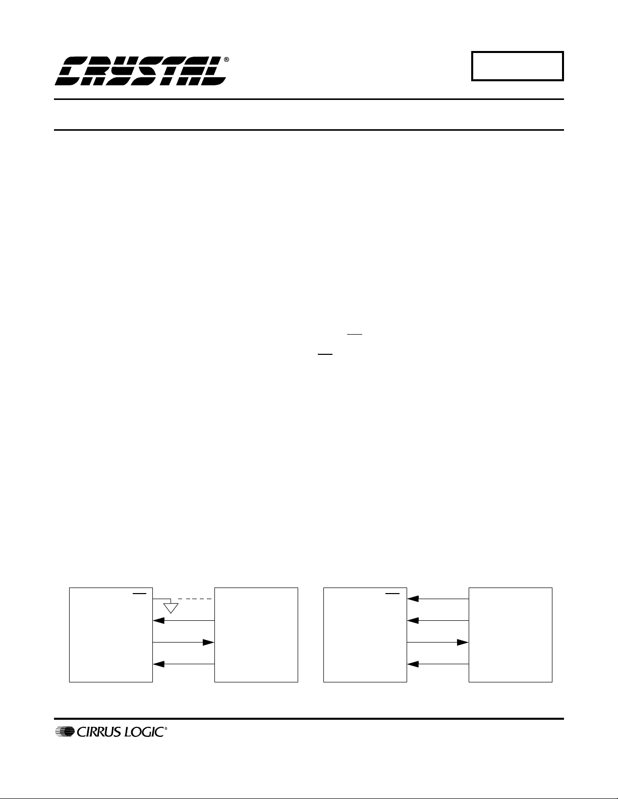
2. ADC DIGITAL INTERFACE
The CS5521/22/23/24/28 interfaces to the
PIC16C84 through either a three-wire or a fourwire interface. Figure 1 depicts the interface between the two devices. Though this software was
written to interface to Port A (RA) on the
PIC16C84 with a four-wire interface, the algorithms can be easily modified to work with the
three-wire format.
The ADC’s serial port consists of four control
lines: CS, SCLK, SDI, and SDO.
CS, Chip Select, is the control line which enables
access to the serial port.
SCLK, Serial Clock, is the bit-clock which controls
the shifting of data to or from the ADC’s serial
port.
SDI, Serial Data In, is the data signal used to transfer data from the PIC16C84 to the ADC.
SDO, Serial Data Out, is the data signal used to
transfer output data from the ADC to the
PIC16C84.
3-Wire Interface 4-Wire Interface
CS5521/22/23/24/28
CS
SDI
SDO
SCLK
P.O. Box 17847, Austin, Texas 78760
(512) 445 7222 FAX: (512) 445 7581
http://www.cirrus.com
PIC16C84
NC (RA0)
RA1
RA2
RA3
Figure 1. 3-Wire and 4-Wire Interfaces
CS5521/22/23/24/28
SDO
SCLK
Copyright Cirrus Logic, Inc. 1999
(All Rights Reserved)
CS
SDI
PIC16C84
RA0
RA1
RA2
RA3
NOV ‘99
AN130REV2
1
Page 2
AN130
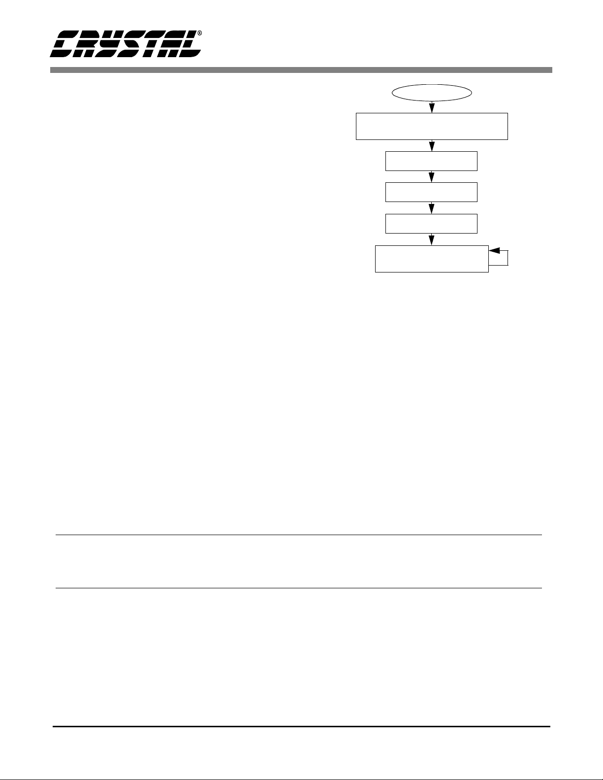
3. SOFTWARE DESCRIPTION
This note presents algorithms to initialize the
PIC16C84 and the CS5521/22/23/24/28, perform
calibrations, modify the CS5521/22/23/24/28’s internal registers, and acquire a conversion. Figure 2
depicts a block diagram of the main program structure. While reading this application note, please refer to Section 8. “APPENDIX: PIC16C84
Microcode to Interface to the
CS5521/22/23/24/28” on page 6 for the code listing.
3.1 Initialize
Initialize is a subroutine that configures Port A
(RA) on the PIC16C84 and places the serial port of
the CS5521/22/23/24/28 into the command state.
RA’s data direction is configured as depicted in
Figure 1 by writing to the TRISA register (for more
information on configuring ports, see the
PIC16C84 Data Sheet). The controller then enters
a number of delay states to allow the appropriate
time for the ADC’s oscillator to start up and stabilize (oscillator start-up time for a 32.768 KHz crystal is typically about 500ms). Finally, the ADCs
serial port is reset by sending fifteen bytes of logic
1’s followed by a single byte with its LSB at logic
0 to SDI (the serial port is initialized after any power-on reset, and this software re-initializa tion is for
demonstration purposes) Once the proper sequence
of bits has been received, the serial port on the
START
INITIALIZE
MICROCONTROLLER & ADC
WRITE CSRs
SELF-OFFSET CAL.
MODIFY GAIN
ACQUIRE CONVERSION
Figure 2. CS5521/22/23/24/28 Software Flowchart
ADC is in the command state, where it waits for a
valid command.
3.2 Write Channel Setup Registers
The subroutine write_csrs is an example of how to
write to the CS5521/22/23/24/28’s Channel Setup
Registers (CSRs). For this example, two CSRs
(four Setups) are written. The number of CSRs to
be accessed is determined by the Depth Pointer bits
(DP3-DP0) in the configuration register. The
Depth Pointer bits are set to “0011” to access the
two CSRs. The value “0011” is calculated by taking the number of Setups to be accessed and subtracting 1. Because each CSR holds two Setups,
this number must always be an odd value, that is,
Contacting Cirrus Logic Support
For a complete listing of Direct Sales, Distributor, and Sales Representative contacts, visit the Cirrus Logic web site at:
http://www.cirrus. com/corporat e/contact s/
SPI is a trademark of Motorola.
MICROWIRE is a trademark of National Semiconductor.
MPLAB and MPASM are trademarks of Microchip.
Cirrus Logic, Inc. has made best efforts to ensure that the information contained in this document is accurate and reliable. However, the in-
formation is subject to change without notice and is provided “AS IS” without warranty of any kind (express or implied). No re sponsibility is
assumed by Cirrus Logic, Inc. for the use of this information, nor for infringements of patents or other rights of third parties. This document
is the property of Cirrus Logic, Inc. and implies no license under patents, copyrights, trademarks, or trade secrets. No part of this publication
may be copied, reproduced, stored in a retrieval system, or transmitted, in any form or by any means (electronic, mechanical, photographic,
or otherwise). Furthermore, no part of this publication may be used as a basis for manufacture or sale of any items without the prior written
consent of Cirrus Logic, Inc. The names of products of Cirrus Logic, Inc. or other vendors and suppliers appearing in this document may be
trademarks or service marks of their respective owners which may be registered in some jurisdictions. A list of Cirrus Logic, Inc. trademarks
and service marks can be found at http://www.cirrus.com.
2 AN130REV2
Page 3

AN130
DP0 must always be logic 1 when reading and writing the CSRs. To modify the Depth Pointer bits, the
configuration register is read to prevent corruption
of other bits. After the read_register routine is run
with the command 0x0B (HEX), the DP3-DP0 bits
are masked to “0011”. Then, the updated information is written back into the ADC with the command 0x03 (HEX) using the write_register routine.
After the depth pointer bits are set correctly, the
CSR information is written to the ADC. The command 0x05 (HEX) is sent to the ADC to begin the
write sequence (to read the CSRs, the command
would be 0x0D). At this point, the ADC is expecting to receive information for two 24-bit CSRs, or
48 bits, based on the Depth Pointer bits. The first
CSR is written with a value of 0x000000 (HEX).
This sets Setup 1 and Setup 2 both to convert bipolar, 100mV signals on physical channel 1 (PC1) at
an output word rate (OWR) of 15 Hz, and latch pins
A1-A0 equal to “00”. The second CSR is written
with the value 0x4C0105 (HEX). This sets Setup 3
to convert a bipolar, 100mV signal on PC2 at a
101.1 Hz OWR, with latch pins A1-A0 at “01”.
This also sets Setup 4 to convert a unipolar, 25mV
input signal at 15 Hz on PC3, with out put latch pins
A1-A0 set to “00”.
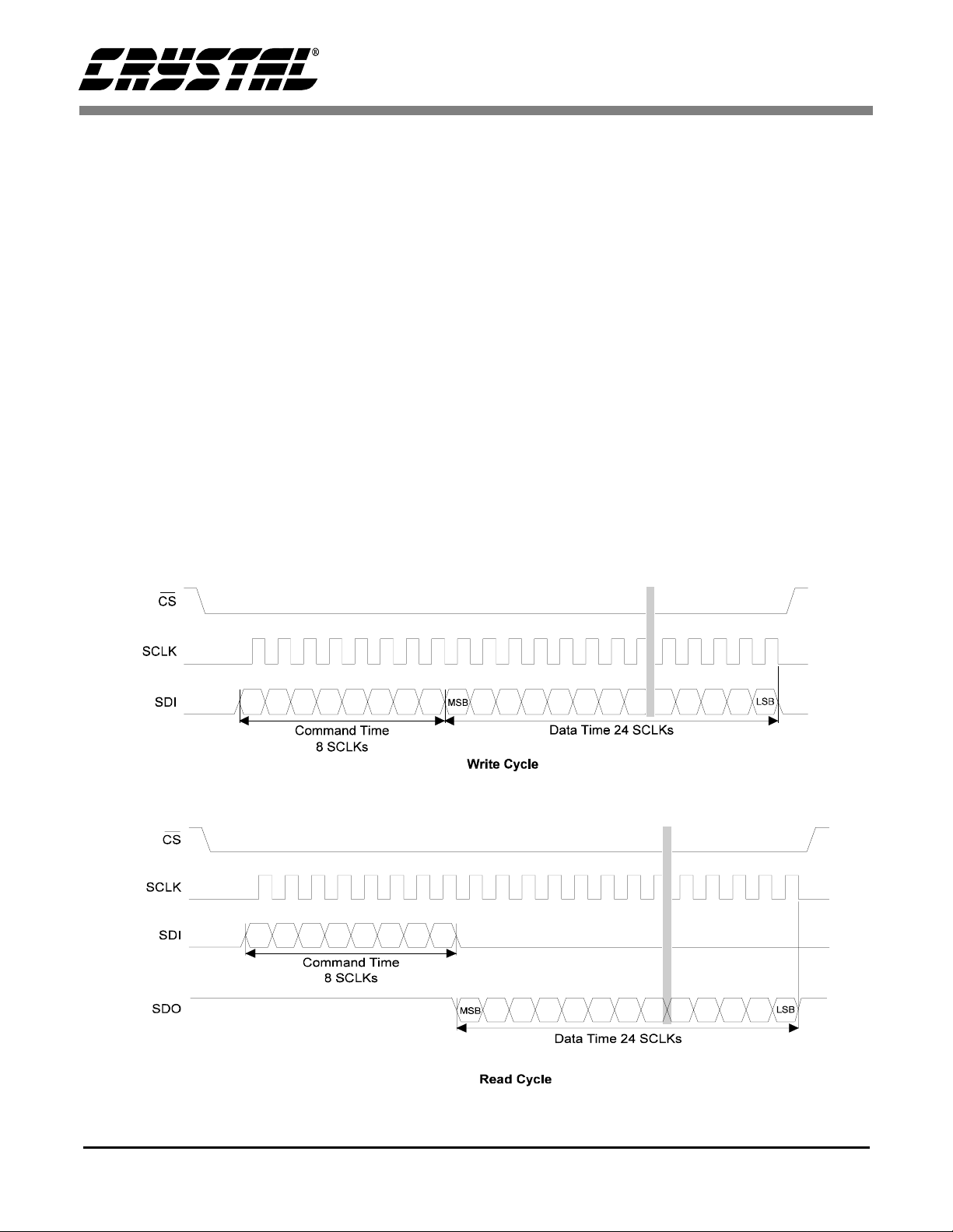
3.4 Read/Write Gain Register
The routine modify_gain provides an example of
how to modify the ADC’s internal gain registers.
To modify the gain register the command byte and
data byte variables are written with the appropriate
information. Modify_gain then calls the subroutine
write_register, which uses these variables to set the
contents of Physical Channel 1 (PC1)’s gain register to 0x800000 (HEX). The write_register routine
calls the send_byte algorithm four times, once to
send the command byte, and three more times to
send the three data bytes. Send_byte is a subroutine
used to ‘bit-bang’ a byte of information from the
PIC16C84 to the CS5521/22/23/24/28. A byte is
transferred one bit at a time, MSB (most significant
bit) first, by placing a bit of information on RA1
(SDI) and then pulsing RA3 (SCLK). The byte is
transferred by repeating this process eight times.
Figure 3 depicts the timing diagram for the writecycle in the CS5521/22/23/24/28’s serial port. It is
important to note here that this section of the code
demonstrates how to write to the gain register of
PC1. It does not perform a gain calibration. To
write to the other internal registers of the ADC, follow the procedures outlined in the
CS5521/22/23/24/28 data sheet.
3.3 Self-Offset Calibration
Calibrate is a subroutine that performs a self-offset
calibration using Setup 1. Calibrate does this by
sending the command 0x81 (HEX) to the ADC.
This tells the ADC to perform a self-offset calibration using Setup 1 (see the CS5521/22/23/24/28
Data Sheet for information on performing offset or
gain calibrations using other Setups). Once the
command has been sent, the controller polls RA2
(SDO) until it falls, indicating that the calibrat ion is
complete. Note that although calibrations are done
on a specific Setup, the offset or gain register that
is modified belongs to the physical channel referenced by that Setup.
AN130REV2 3
To read the value in the gain register of PC1, the
command byte is loaded with the value 0x0A
(HEX), and the read_register routine is called. It
duplicates the read-cycle timing diagram depicted
in Figure 4. Read_register asserts CS (RA0). The n
it calls send_byte once to transfer the command-
byte to the CS5521/22/23/24/28. This places the
converter into the data state where it waits until
data is read from its serial port. Read_register then
calls receive_byte three times and transfers three
bytes of information from the CS5521/22/23/24/28
to the PIC16C84. Similar to send_byte,
receive_byte acquires a byte one bit at a time, MSB
first. When the transfer is complete, the variables
high_byte, mid_byte, and low_byte contain the value present in PC1’s 24-bit gain register.
Page 4
AN130
3.5 Acquire Conversion
To acquire a conversion the subroutine convert is
called. For single conversions on one physical
channel, the MC (multiple conversion) and the LP
(loop) bits in the configuration register must be logic 0. To prevent corruption of the configuration
register, convert instructs the PIC16C84 to read
and save the contents. This information is stored in
the variables HIGHBYTE, MIDBYTE and LOWBYTE. Then the MC, LP, and RC (read conver t)
bits are masked to logic 0, and the new information
is written back to the ADC’s co nfiguration regis ter.
A conversion is initiated on Setup 1 by sending the
command 0x80 to the converter. At this time, the
controller polls RA2 (SDO) until it falls to a logic
0 level (see Figure 5). After SDO falls, convert applies a logic 0 to RA1 (SDI) and pulses RA3
(SCLK) eight times to initiate the data transfer
from the ADC. The PIC16C84 then reads the conversion data word by calling receive_byte three
times. Figure 6 depicts how the 16 or 24-bit data
word is stored in the memory locations HIGHBYTE, MIDBYTE, and LOWBYTE.
4. MAXIMUM SCLK RATE
An instruction cycle in the PIC16C84 consists of
four oscillator periods, or 400ns if the microcontroller’s oscillator frequency is 10 MHz. Since the
CS5521/22/23/24/28’s maximum SCLK rate is
2MHz, additional no operation (NOP) delays may
be necessary to reduce the tra nsfer rate if the microcontroller system requires higher rate oscillators.
5. SERIAL PERIPHERAL INTERFACE
When using a built-in Serial Peripheral Interface
(SPI) port, the designer must pay special attention
to how the port is configured. Most SPI ports allow
Figure 3. Write-Cycle Timing
Figure 4. R ead-Cycle Timing
4 AN130REV2
Page 5
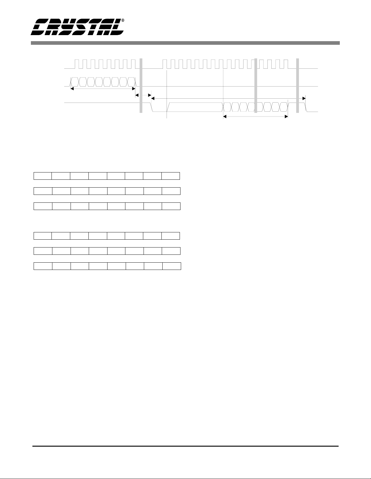
SCLK
SDI
*
t
ommand Time
C
8SCLKs
DO
S
td = XIN/OWR clock cycles for each conversion except the
*
first conversion which will take XIN/OWR + 7 clock cycles
d
Data SDO Continuous Conversion Read
Figure 5. Conversion/Acquisition Cycle Timing
SCLKs Clear SDO Flag
8
AN130
IN/OWR
X
Clock Cycles
SB
M
ata Time
D
24 SCLKs
SB
L
MSB High-Byte
D23 D22 D21 D20 D19 D18 D17 D16
Mid-Byte
D15 D14 D13 D12 D11 D10 D9 D8
Low-ByteLSB
D7 D6 D5 D4 D3 D2 D1 D0
A) 24-Bit Conversion Data Word (CS5522/24/28)
MSB High-Byte
D15 D14 D13 D12 D11 D10 D9 D8
Mid-Byte
D7 D6 D5 D4 D3 D2 D1 D0
Low-Byte
1110CI1CI0ODOF
B) 16-bit Conversion Data Word (CS5521/23)
0 - always zero, 1 - always 1
CI1, CI0 - Channel Indicator Bits
OD - Oscillation Detect, OF - Overflow
Figure 6. Bit Representation/Storage in the PIC16C84
for a selectable clock polarity. However, many do
not have the capability to select the clock’s phase.
When using a microcontroller with both features,
the clock polarity should be set to idle low, and the
clock phase should be set to begin clocking in the
middle of the data bits. For an SPI port without the
variable clock phase feature to function properly
with the CS5521/22/23/24/28, the clock polarity
needs to be set to idle high, and the ADC’s serial
port must be re-initialized anytime new information is transmitted bet ween t he mic rocontroller and
the converter.
6. DEVELOPMENT TOOL DESCRIPTION
The code in this application note was developed
with MPLABTM, a development package from Microchip, Inc. It was written in Microchip assembly
and compiled with the MPASMTM assembler.
7. CONCLUSION
This application note presents an example of how
to interface the CS5521/22/23/24/28 to the
PIC16C84. It is divided into two main sections:
hardware and software. The hardware section illustrates both a three-wire and a four- wire interface.
The three-wire interface is SPI™ and MICROW-
IRE™ compatible. The software, developed using
tools from Microchip, Inc., illustrates how to initialize the converter and microcontroller, write to
the CSRs, write and read the ADC’s internal registers, perform calibrations, and acquire conversions.
The software is modularized and provides important subroutines such as write_register,
read_register, write_csrs and convert, which were
all written in PIC assembly language.
The software described in the note is included in
Section 8. “APPENDIX: PIC16C84 Microcode to
Interface to the CS5521/22/23/24/28” on page 6.
AN130REV2 5
Page 6

AN130
8. APPENDIX: PIC16C84 MICROCODE TO INTERFACE TO THE CS5521/22/23/24/28
;*****************************************************************************
;* File: 55221684.ASM
;* Date: November 1, 1999
;* Revision: 1
;* Processo r :PI C16C84
;* Program entry point at routine "main". Entry point address is 0x05.
;*****************************************************************************
;* This program is designed to provide examples of how to interface the
;* CS5521/22/23/24/28 ADCs to a PIC16C84 Microcontroller. The software handles all
;* of the serial communications between the controller and the ADC to perform
;* system calibration and acquire 24 and 16-bit conversion words.
;*****************************************************************************
;*** Memory Map Equates ***
STATUS equ 0x03 ; STATUS register
PORTA equ 0x05 ; I/O Port A address
TRISA equ 0x85 ; Port A Data Direction Co ntrol Latch
CARRY equ 0x00 ; Carry Bit in STATUS
RP0 equ 0x05 ; Register Bank Select Bit in STATUS
CS equ 0x00 ; Port A bit 0 - Chip Select
SDI equ 0x01 ; Port A bit 1 - Serial Data In
SDO equ 0x02 ; Port A bit 2 - Serial Data Out
SCLK equ 0x03 ; Port A bit 3 - Serial Clock
HIGHBYTE equ 0X0C ; Upper 8 Bits of Conversion Registe r
MIDBYTE equ 0x0D ; Middle 8 Bits of Conversion Register
LOWBYTE equ 0x0E ; Lowest 8 bits of Conversion Register
COMMAND equ 0x0F ; Command Byte RAM location
TEMP equ 0x10 ; Temporary Data storage RAM location
COUNT equ 0x11 ; Software Counter RAM location
SERI_DATA equ 0x12 ; Serial Data RAM location
;*****************************************************************************
;* Program Code
;************* *** *** ********************************* *** *** *******************
processor 16C84 ; Set Processor Type
org 0x00 ; Reset Vector Location
goto main ; Start at "main" routine
;*****************************************************************************
6 AN130REV2
Page 7

;* Routine - main
;* Input - none
;* Output - none
;* This is the entry point to the program, as well as the central loop.
;*****************************************************************************
org 0x05 ; program memory beginning location
main
;*** Initialize and Calibrate System ***
CALL initialize ; Initialize the System
CALL write_csrs ; Modify the Channel Setup Registers
CALL calibrate ; Calibrate ADC Offset
CALL modify_gain ; Write and Read gain register
;*** Loop to perform continuous single conversions ***
mloop: CALL convert ; Obtain conversions from ADC
goto mloop ; Keep looping
AN130
;*** End main ***
;*****************************************************************************
;* Subroutines
;************* ********************************** ***************** *************
;************* ********************************** ***************** *************
;* Routine - initialize
;* Input - none
;* Output - none
;* This subroutine initializes Port A to interface to the CS5521/22/23/24/28 ADC.
;* A time delay is provided to allow for the ADC oscillator to power up.
;* Typically, a 32.768 KHz crystal has a start-up time of about 500ms.
;* Additionally, 1003 XIN cycles are delayed for the ADC’s power-on reset
;* after the crystal has stabilized. The total delay is 660ms upon system
;* power-up, assuming that the microcontroller has no start-up delay.
;*****************************************************************************
initialize CLRF PORTA ; Clear Port A Output data latches
BSF STATUS, RP0 ; Select Register Bank 1 - control
MOVLW 0x04 ; Directional Values for Port A:
MOVWF TRISA ; RA2 = input, RA0-1 & 3-4 = output
BCF STATUS, RP0 ; Select Register Bank 0 - normal
MOVLW 0x32 ; Load W for delay count
CALL delay ; Delay 1003 XIN cycles
AN130REV2 7
Page 8

MOVLW 0xFF ; Load W for new delay count
CALL delay ; Delay for Oscillator start-up 158ms
CALL delay ; Delay for Oscillator start-up 158ms
CALL delay ; Delay for Oscillator start-up 158ms
CALL delay ; Delay for Oscillator start-up 158ms
;*** ADC Serial Port Initialization ***
MOVLW 0x0F ; Load W with a value of 15
MOVWF TEMP ; Loop count variable = TEMP
BCF PORTA, CS ; Clear CS to enable ADC
loop: MOVLW 0xFF ; Load W with all 1’s
CALL send_byte ; send all 1’s to ADC
DECFSZ TEMP, 1 ; loop through to send 15 bytes of all 1’s
goto loop
MOVLW 0xFE ; Load W with last byte - ’11111110’
CALL send_byte ; send final initialize byte to ADC
BSF PORTA, CS ; Set CS to disable ADC
RETURN ; Exit to "main"
AN130
;*****************************************************************************
;* Routine - calibrate
;* Input - none
;* Output - none
;* This subroutine tells the ADC to perform self-offset calibration on Setup 1
;*****************************************************************************
calibrate MOVLW 0x81 ; Command for Self-Offset Calibration
BCF PORTA, CS ; Enable ADC
CALL send_byte ; Send Calibration Command to ADC
poll_sdo1: BTFSC PORTA, SDO ; Wait until SDO falls to indicate
goto poll_sdo1 ; calibration completion.
BSF PORTA, CS ; Disable ADC
RETURN ; Exit to "main"
;*****************************************************************************
;* Routine - modify_gain
8 AN130REV2
Page 9

;* Input - none
;* Output - none
;* This subroutine writes to and reads from the gain register on ph ysical
;* channel 1.
;************* ****************************************************************
modify_gain MOVLW 0x02 ; Command to write Gain register
MOVWF COMMAND ; Set command byte
MOVLW 0x80 ; High byte information
MOVWF HIGHBYTE ; Set high byte
CLRF MIDBYTE ; Set middle byte
CLRF LOWBYTE ; Set low byte
CALL write_register ; Write 0x800000 to Gain Register
MOVLW 0x0A ; Command to read Gain Regi ster
MOVWF COMMAND ; Set Command byte
CALL read_register ; Read data from the Gain Register
RETURN ; Exit
AN130
;*****************************************************************************
;* Routine - write_csrs
;* Input - none
;* Output - none
;* This subroutine is used to modify the information in the Channel Setup
;* Registers. It first changes the depth pointer bits in the ADCs config.
;* register to reflect the number of CSRs to be written, and then writes to
;* the appropriate CSRs
;************* ****************************************************************
write_csrs MOVLW 0x0B ; Co m mand to read Config. Register
MOVWF COMMAND ; set command byte
CALL read_register ; read the config. register
;*** Mask DP3-DP0 to access two CSRs (four Setups) ***
MOVLW 0x3F ; mask DP3-DP2 low
ANDWF MIDBYTE, 1 ; change DP3 and DP2
MOVLW 0x30 ; mask DP1-DP0 high
IORWF MIDBYTE, 1 ; change DP1 and DP0
MOVLW 0x03 ; Command to write config. register
MOVWF COMMAND ; set command byte
CALL write_register ; Change Depth Pointer Bits
;*** Write to CSRs - note, the ADC expects information for the
; number CSRs indicated in the Depth Bits (DP3-0 in the
; configuration register) so all of the CSRs are
; written at this time ***
AN130REV2 9
Page 10

MOVLW 0x05 ; Command to write CSR s
BCF PORTA, CS ; select the ADC
CALL send_byte ; send command byte to ADC
;*** Setup CSR #1 - Setups 1 and 2
; setting both to default value of ’000’
; (A1-A0 = 00, Physical Channel = 1, OWR = 15Hz,
; input V-range = 100mV, Bipolar Measurement mode) ***
MOVLW 0x00 ; all zeros
CALL send_byte ; send first byte
CALL send_byte ; send second byte
CALL send_byte ; send third byte
;*** Setup CSR #2 - Setups 3 and 4
; setting Setup 3 to ’4C0’ and Setup 4 to ’105 ’
; Setup 3 Settings - (A1-A0 = 01, Physical Channel = 2,
; OWR = 101.1 Hz, input V-range = 100mV, Bipolar)
; Setup 4 Settings - (A1-A0 = 00, Physical Channel = 3,
; OWR = 15 Hz, input V-range = 25mV, Unipolar)
AN130
MOVLW 0x4C ; first byte of info
CALL send_byte ; send first byte
MOVLW 0x01 ; second byte of info
CALL send_byte ; send second byte
MOVLW 0x05 ; third byte of info
CALL send_byte ; send last byte
BSF PORTA, CS ; de-select the ADC
RETURN ; exit
;*****************************************************************************
10 AN130REV2
Page 11

;* Routine - convert
;* Input - none
;* Output - 24-bit Conversion Results in memory locations HIGHBYTE, MIDBYTE
;* and LOWBYTE.
;* The Algorithm itself will only perform a single
;* conversion using Setup 1. For mu ltiple continuous
;* conversions, or for conversions using other setups, the routine
;* must be modified. (see the CS5521/22/23/24/28 data sheet for more info)
;*****************************************************************************
convert MOVLW 0x0B ; Command to read Configuration Reg.
MOVWF COMMAND ; Set Command Byte
CALL read_register ; Read Config. Register Information
MOVLW 0xF8 ; Load mask info into W
ANDWF HIGHB YTE, 1; Mask MC, LP, and RC to 0
MOVLW 0x03 ; Command to write Configuration Reg.
MOVWF COMMAND ; Set Command Byte
CALL write_register ; Write C onf ig. Register with new info
; *** Receive Conversion Data ***
AN130
BCF PORTA, CS ; Enable ADC
MOVLW 0X80 ; Command for conversion using Setup 1
CALL send_byte ; send command byte
poll_sdo2: BTFSC PORTA, SDO; Wa it until SDO falls to indicate
goto poll_sdo2 ; conversion completion
MOVLW 0X00 ; Command to start data output
CALL send_byte ; send command
CALL receive_byte ; Receive data...
MOVWF HIGHBYTE ; High Byte 1st..
CALL receive_byte
MOVWF MIDBYTE ; then the Middle Byte..
CALL receive_byte
MOVWF LOWBYTE ; and finally the Low Byte.
BSF PORTA, CS ; Disable ADC
RETURN ; Exit to "main"
;*****************************************************************************
AN130REV2 11
Page 12

;* Routine - write_register
;* Input - COMMAND, HIGHBYTE, MIDBYTE, LOWBYTE
;* Output - none
;* This subroutine writes to the internal registers of the CS55/212 2/ 23/24/28
;*****************************************************************************
write_register BCF PORTA, CS ; Enable ADC
MOVF COMMAND, 0; Load W with Command byte
CALL send_byte ; Send command info
MOVF HIGHBYTE, 0; Load W with high byte
CALL send_byte ; Send high byte first..
MOVF MIDBYTE, 0 ; Load W with middle byte
CALL send_byte ; Then the middle byte..
MOVF LOWBYTE, 0 ; Load W with low byte
CALL send_byte ; .. and then the low byte last.
BSF PORTA, CS ; Disable ADC
RETURN ; Exit Subroutine
;*****************************************************************************
;* Routine - read_register
;* Input - COMMAND
;* Output - HIGHBYTE, MIDBYTE, LOWBYTE
;* This subroutine reads from the internal regis ters of the CS5521/22/23/24/28
;*****************************************************************************
AN130
read_register BCF PORTA, CS ; Enable ADC
MOVF COMMAND, 0; Load W with Command Byte
CALL send_byte ; Send Command info
CALL receive_byte ; receive High byte first..
MOVWF HIGHBYTE ; Move W to HIGHBYTE
CALL receive_byte ; and then the middle byte..
MOVWF MIDBYTE ; Move W to MIDBYTE
CALL receive_byte ; and finally the Low byte.
MOVWF LOWBYTE ; Move W to LOWBYTE
BSF PORTA, CS ; Disable ADC
RETURN ; Exit Subroutine
;*****************************************************************************
12 AN130REV2
Page 13

;* Routine - send_byte
;* Input - Byte stored in W register
;* Output - none
;* This subroutine sends a byte, one bit at a time, MSB first, to the ADC
;*****************************************************************************
send_byte MOVWF SERI_DATA ; Move W to SERI_DATA
MOVLW 0x08 ; Set COUNT to 8
MOVWF COUNT ; to trasnsmit each bit individually
bitloop1: RLF SERI_DATA, 1 ; Rotate SERI_DATA to send MSB first
BTFSC STATUS, CARRY ; If bit is low, skip next instruction
BSF PORTA, SDI ; If high, set SDI
BTFSS STATUS, CARRY ; If bit is high, skip next instr.
BCF PORTA, SDI ; If low, clear SDI
BSF PORTA, SCLK ; Toggle SCLK High
BCF PORTA, SCLK ; Toggle SCLK Low
DECFSZ COUNT, 1 ; Go to next bit unless done
goto bitloop1
BCF PORTA, SDI ; Return SDI to low state
RETURN ; Exit Subroutine
AN130
;*****************************************************************************
;* Routine - receive_byte
;* Input - none
;* Output - Byte stored in W register
;* This subroutine receives a byte, one bit at a time, MSB first, from the ADC
;*****************************************************************************
receive_byte MOVLW 0x08 ; Set COUNT to 8
MOVWF COUNT ; to receive each bit individually
bitloop2: BTFSC PORTA, SDO ; If Bit is low, skip next instruction
BSF STATUS, CARRY ; Otherwise, set carry bit
BTFSS POR TA, SDO ; If Bit is high, skip next instruction
BCF STATUS, CARRY ; Otherwise, clear carry bit
RLF SERI_DATA, 1 ; Rotate Carry into SERI_DATA, MSB first
BSF PORTA, SCLK ; Toggle SCLK High
BCF PORTA, SCLK ; Toggle SCLK Low
DECFSZ COUNT, 1 ; Go to next bit unless finished
goto bitloop2
MOVF SERI_DATA, 0 ; Put received byte into W
RETURN ; Exit Subroutine
;*****************************************************************************
AN130REV2 13
Page 14

;* Routine - delay
;* Input - Count in W register
;* Output - none
;* This subroutine delays by using a count value stored in register W. This
;* example was tested using a 10MHz clock (E = 2.5 MHz), thus each
;* cycle is 400ns. This delay is approximately equivalent to:
;* (400ns)*(1536)*(count value in W) - A count of 720 provides a 445ms delay
;*****************************************************************************
delay MOVWF COUNT ; Move delay value to COUNT
outlp: CLRF TEMP ; TEMP used for inner loop counter
innlp: NOP ; 1 cycle - 400ns
NOP ; 2 cycles - 800ns
NOP ; 3 cycles - 1.2 us
NOP ; 4 cycles - 1.6 us
DECFSZ TEMP, 1 ; Decrement TEMP and loop 256 times
goto innlp
DECFSZ COUNT, 1 ; Decrement COUNT and loop
goto outlp
RETURN ; Exit delay
AN130
;*****************************************************************************
;* Interrupt Vectors
;************* *** ********************************** ** *************************
NOT_USEDRETFIE
ORG 0x04 ; originate interrupt vector here
goto NOT_USED ; no interrupts enabled
end ; end program listing
14 AN130REV2
Page 15

• Notes •
Page 16

 Loading...