

Page 1
AN48
Application Note
DESIGNNOTESFORA2-POLEFILTERWITH
DIFFERENTIAL INPUT
by Steven Green
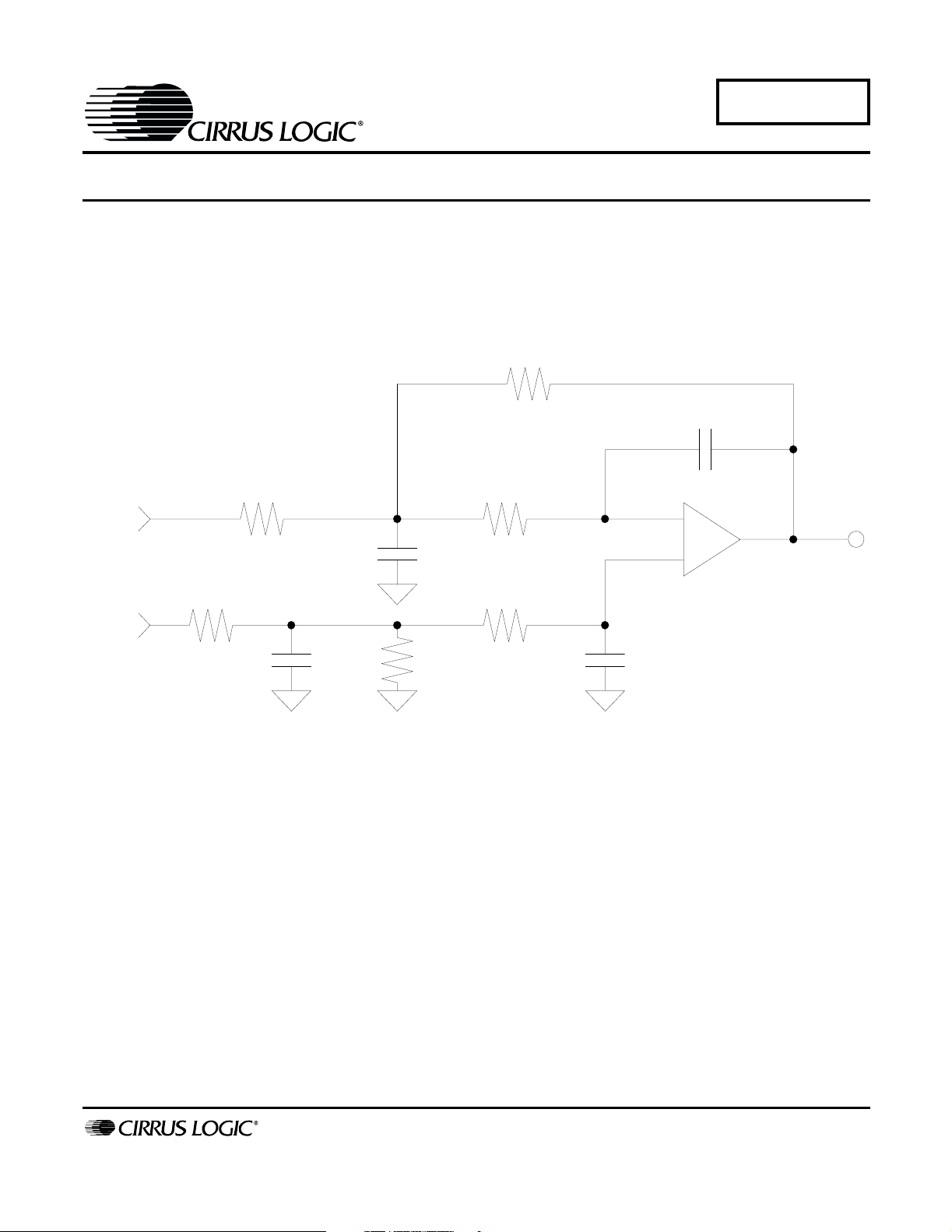
AIN-
AIN+
R1
R4
R1
R3
C2
C2
Figure 1. 2-Pole Low-Pass Filter with Differential Input
R4
R3
C5
_
+
C5
1. Introduction
Many of today’s Digital-to-Analog Converters
(DACs) require a circuit that has a differential input
and will remove common-mode errors, reduce the
out-of-band noise produced by the delta-sigma
modulator and produce a single-ended output. The
circuit in Figure 1 includes a differential input and a
two-pole analog filter to achieve these design requirements. This application note outlines the design steps required to select component values.
www.cirrus.com
Copyright Cirrus Logic, Inc. 2003
(All Rights Reserved)
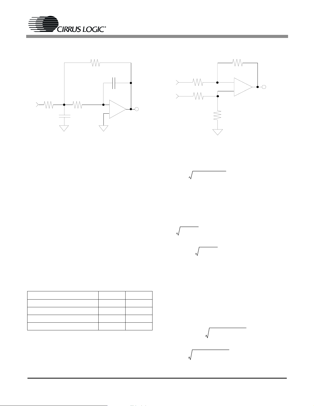
Notice the similarities between Figure 1 and the
multiple-feedback low-pass filter shown in
Figure 2. The 2-Pole Low-Pass Filter with Differential Input is easily designed using the design equations for the multiple-feedback low-pass filter. Also,
notice the similarities between Figure 1 and
Figure 3. The differential input function is accomplished by simply duplicating the component values generated in the filter design
MAR ‘03
AN48REV2
1
Page 2
AN48
R4
C5
R3R1
C2
Figure 2. Multiple-Feedback Low-Pass
Filter
_
+
2. Design Steps
Step 1: Determine the required pass band gain,
H
. The circuit parameters require that the magni-
o
tude of H
also negative due to the inverting op-amp configuration.
be greater than or equal to one. Hois
o
R4
R1
R1
Figure 3. Differential Input Circuit
_
+
R4
Step 4: Select convenient values for C5 and C2.
Notice in Step 5 that K and H
such that is real.
Step 5: Given F
ζ2K 1 Ho–()–
,C2,C5, alpha and beta, cal-
c,Ho
must be selected
o
culate R1,R2 and R3 using the following equa-
tions.
Step 2: Determine the minimum input impedance.
Step 3: Select the desired filter type, Butterworth,
Bessel, etc. and the corner frequency, F
,forthefi-
c
nal design. The filter response and corner frequency determine the pass band phase and amplitude
response. The filter type determines the pole-locations and therefore alpha and beta. Table 1 lists
the normalized pole locations for several filter
types.
Table 1: Normalized Pole Locations
FILTER TYPE αβ
Butterworth 0.7071 0.7071
Bessel 1.1030 0.6368
0.01 dB Chebyshev 0.6743 0.7075
0.1 dB Chebyshev 0.6104 0.7106
----------------------=
α
2πFcα2β2+=
C
5
-----=
C
2
R
--------------=
--------------------------------------------------------------------=
ω
oC2
α
2β2
+
4
Ho–()
1
ζζ2K 1 Ho–()–±[]
ζ
ω
o
K
R
1
R
3
ζζ2K 1 Ho–()–±
R
-------------------------------------------------=
4
ω
oC5
⋅
2
Page 3

AN48
Step 6: Review the resistor and capacitor values.
It is desirable to keep the capacitor values sufficiently large to minimize the effects of stray capacitance. It may be necessary to adjust the capacitor
values chosen in Step 4 to achieve this requirement. Also verify that R1 is larger than the minimum required input impedance.
Step 7: The resistor values calculated in Step 5
are generally not standard values. Select standard
values which are nearest the calculated values.
This should not create a large change in the filter
characteristics since metal film resistors are available in approximately 2.5% increments which allows for component selection near the calculated
values. However, it is advisable to calculate the actual filter parameters, using the selected values,
using the equations in Step 5.
Step 8: The conversion from the singled-ended circuit to the differential circuit requires duplicating
the values of R
1,C2,R3,R4 and C5 in the non-in-
verting input, as shown in Figure 1.
3. Design Example
Step 1: The required pass band gain, Ho,is-1for
this example.
with a corner frequency of 50 kHz attenuates the
signal at 20 kHz by approximately 0.1 dB and has
nearly ideal phase linearity within the audio band.)
F
=50kHz
c
alpha = .7071
beta = .7071
Step 4: Select convenient values for C
5 and C2.
C5 = 220 pF
C
2 = 1000 pF
Step 5: Given F
culate R
R
1 = 13.77 kΩ
1,R3 and R4.
,Ho,C2,C5, alpha and beta, cal-
c
R3 = 3.343 kΩ
R
4 = 13.77 kΩ
Step 6: Review the filter component values and filter parameters. Verify that R
1 is greater than 10 kΩ
and the capacitor values are sufficiently large to
negate stray capacitance effects.
Step 7: Select standard resistor values which are
nearest the calculated values.
R
1 = 13.7 kΩ
R
3 =3.32kΩ
R4 = 13.7 kΩ
Step 2: Minimum input impedance is 10 kΩ.
Step 3: Select a Butterworth response with a cor-
ner frequency of 50kHz. (A two-pole Butterworth
13.7 k
Ω
13.7 k
Ω
3.32 k
Ω
1000 pF
Figure 4. 2-Pole Multiple Feedback Filter Design
Step 8: The conversion from the singled-ended to
the differential circuit requires duplicating the values of R
1,C2,R3,R4 and C5 in the non-inverting
input as shown in Figure 4 and 5.
220 pF
_
+
3
Page 4

13.7 k
AN48
Ω
220 pF
AIN-
13.7 k
13.7 k
Ω
1000 pF
Ω
3.32 k
3.32 k
Ω
_
+
Ω
AIN+
1000 pF
Ω
13.7 k
Figure 5. 2-Pole Filter with Differential Input
220 pF
.
REFERENCES
[1] C. L. Lindquist, “Active Network Design with Signal Filtering Applications”, Steward & Sons
[2] A. B. Williams, “Electronic Filter Design Handbook”, McGraw-Hill
[3] “Reference Data for Radio Engineers” (Fourth Edition), International Telephone and Telegraph Corporation
Contacting Cirrus Logic Support
For all product questions and inquiries contact a Cirrus Logic Sales Representative.
To find one nearest you go to www.cirrus.com
IMPORTANT NOTICE
Cirrus Logic, Inc. and its subsidiaries (“Cirrus”) believe that the information contained in this document is accurate and reliable. However, the information is subject
to change without notice and is provided “AS IS” without warranty of any kind (express or implied). Customers are advised to obtain the latest version of relevant
information to verify, before placing orders, that information being relied on is current and complete. All products are sold subject to the terms and conditions of sale
supplied at the time of order acknowledgment, including those pertaining to warranty, patent infringement, and limitation of liability. No responsibility is assumed by
Cirrus for the use of this information, including use of this information as the basis for manufacture or sale of any items, or for infringement of patents or other rights
of third parties. This document is the property of Cirrus and by furnishing this information, Cirrus grants no license, express or implied under any patents, mask work
rights, copyrights, trademarks, trade secrets or other intellectual property rights. Cirrus owns the copyrights associated with the information contained herein and gives
consent for copies to be made of the information only for use within your organization with respect to Cirrus integrated circuits or other parts of Cirrus. This consent
does not extend to other copying such as copying for general distribution, advertising or promotional purposes, or for creating any work for resale.
An export permit needs to be obtained from the competent authorities of the Japanese Government if any of the products or technologies described in thismaterial
and controlled under the “Foreign Exchange and Foreign Trade Law” is to be exported or taken out of Japan. An export license and/or quota needs to be obtained
from the competent authorities of the Chinese Government if any of the products or technologies described in this material is subject to the PRC Foreign Trade Law
and is to be exported or taken out of the PRC.
CERTAIN APPLICATIONS USING SEMICONDUCTOR PRODUCTS MAY INVOLVE POTENTIAL RISKS OF DEATH, PERSONAL INJURY, OR SEVERE PROPERTY OR ENVIRONMENTAL DAMAGE (“CRITICAL APPLICATIONS”). CIRRUS PRODUCTS ARE NOT DESIGNED, AUTHORIZED OR WARRANTED FOR USE
IN AIRCRAFT SYSTEMS, MILITARY APPLICATIONS, PRODUCTS SURGICALLY IMPLANTED INTO THE BODY, LIFE SUPPORT PRODUCTS OR OTHER CRITICAL APPLICATIONS (INCLUDINGMEDICAL DEVICES, AIRCRAFT SYSTEMS OR COMPONENTS AND PERSONAL OR AUTOMOTIVE SAFETYOR SECURITY
DEVICES). INCLUSION OF CIRRUS PRODUCTS IN SUCH APPLICATIONS IS UNDERSTOOD TO BE FULLY AT THE CUSTOMER'S RISK AND CIRRUS DISCLAIMS AND MAKES NO WARRANTY, EXPRESS, STATUTORY OR IMPLIED, INCLUDING THE IMPLIED WARRANTIES OF MERCHANTABILITY AND FITNESS FOR PARTICULAR PURPOSE, WITH REGARD TO ANY CIRRUS PRODUCT THAT IS USED IN SUCH A MANNER. IF THE CUSTOMER OR CUSTOMER'S
CUSTOMER USES OR PERMITS THE USE OF CIRRUS PRODUCTS IN CRITICAL APPLICATIONS, CUSTOMER AGREES, BY SUCH USE, TO FULLY INDEMNIFY CIRRUS, ITS OFFICERS, DIRECTORS, EMPLOYEES, DISTRIBUTORS AND OTHER AGENTS FROM ANY AND ALL LIABILITY, INCLUDING ATTORNEYS'
FEES AND COSTS, THAT MAY RESULT FROM OR ARISE IN CONNECTION WITH THESE USES.
Cirrus Logic, Cirrus, and the Cirrus Logic logo designs are trademarks of Cirrus Logic, Inc. All other brand and product names in this document may be trademarks
or service marks of their respective owners.
4
Page 5

• Notes •
Page 6

 Loading...