

Page 1
Global LCD Panel Exchange Center
www.panelook.com
One step solution for LCD / PDP / OLED panel application: Datasheet, inventory and accessory!
www.panelook.com
INNOLUX DISPLAY CORPORATION
MT200LW01 V.A LCD MODULE SPECIFICATION
( ) Preliminary Specification
(●) Final Specification
Approved by Checked by Prepared by
Innolux Display Corporation,
No.160 Kesyue Rd., Chu-Nan Site, Hsinchu Science Park,
Chu-Nan 350, Miao-Li County, Taiwan
Tel: 886-37-586000 Fax: 886-37-586060
Document Number: MT200LW01 V.A-DR4-26
Page 2
Global LCD Panel Exchange Center
www.panelook.com
One step solution for LCD / PDP / OLED panel application: Datasheet, inventory and accessory!
www.panelook.com
INNOLUX DISPLAY CORPORATION
MT200LW01 V.A LCD MODULE SPECIFICATION
Department Prepared by Checked by
PD
MKT
EE
ME
TD
RA
Innolux Display Corporation
Document Number: MT200LW01 V.A-DR4-26
Page 3
Global LCD Panel Exchange Center
www.panelook.com
One step solution for LCD / PDP / OLED panel application: Datasheet, inventory and accessory!
www.panelook.com
Version:1.0
Record of Revision
Version Revise Date Page Content
InnoLux copyright
All rights reserved,
Copying forbidden.
1.0 2009/12/16
All First edition to all Final-Spec.
Page 4
Global LCD Panel Exchange Center
www.panelook.com
One step solution for LCD / PDP / OLED panel application: Datasheet, inventory and accessory!
www.panelook.com
SPEC NO.
PAGE
MT200LW01 V.A
4/24
Contents:
A. General Specification
B. Electrical Specifications
1. Pin assignment
2. Absolute maximum ratings
3. Electrical characteristics
a. Typical operating conditions
b. Display color vs. input data signals
c. Input signal timing
d. Display position
e. Backlight driving conditions
C. Optical specifications
D. Reliability test items
E. Safety
F. Display quality
G. Handling precaution
H. Label
I. Mechanical drawings
Appendix
Page 5
Global LCD Panel Exchange Center
www.panelook.com
One step solution for LCD / PDP / OLED panel application: Datasheet, inventory and accessory!
www.panelook.com
16
General specification
NO. Item Specification Remark
1 Display resolution (pixel)
2 Active area (mm)
3 Screen size (inch)
4 Pixel pitch (mm)
5 Color configuration
6 Overall dimension (mm)
7 Weight (g)
8 Surface treatment
SPEC NO.
1600(H) x 900(V),HD+ resolution
442.8(H)x 249.075(V)
20 inches diagonal
0.2768 (H) x 0.2768 (V)
R, G, B vertical stripe
462.8 (H)x272.0(W) x17 (D) (Typ)
1850(Typ)
Anti-Glare, Haze=25%, Hard coating (3H)
PAGE
MT200LW01 V.A
5/24
Note 1
Note 2
9 Power consumption
10 Input color signal
11 Display colors
12 Color saturation
13 Optimum viewing direction
14 Backlight
15 RoHS & Halogen free
16 TC0’5.0
17.85W(Typ)
8 bit LVDS
16.7M (6 bit with Hi-FRC)
72% NTSC
6 o’clock
2 CCFL
RoHS & Halogen free compliance
TC0’5.0 Compliance
Note 1: Depth is 17mm(TYP)+/-0.5mm
Note 2: Glare Option available.
Note 3: Anti-Glare model only.
Note 3
Page 6
Global LCD Panel Exchange Center
www.panelook.com
One step solution for LCD / PDP / OLED panel application: Datasheet, inventory and accessory!
www.panelook.com
SPEC NO.
PAGE
B. Electrical specifications
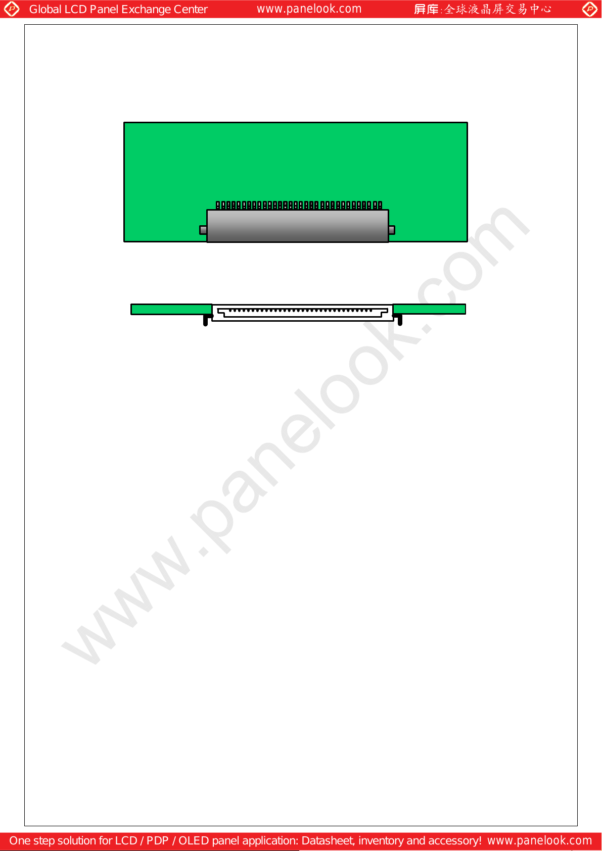
1.Pin assignment
Connector
FOXCONN GS23302-0311S-7F or mechanical interface equivalent connector.
Pin No Symbol Description
Frame VSS Ground
1 RXinO0- -LVDS differential data input, Chan 0-Odd
2 RXinO0+ +LVDS differential data input, Chan 0-Odd
3 RXinO1- -LVDS differential data input, Chan 1-Odd
4 RXinO1+ +LVDS differential data input, Chan 1-Odd
5 RXinO2- -LVDS differential data input, Chan 2-Odd
6 RXinO2+ +LVDS differential data input, Chan 2-Odd
MT200LW01 V.A
6/24
7 VSS Ground
8 RXOC- -LVDS differential Clock input (Odd)
9 RXOC+ +LVDS differential Clock input (Odd)
10 RXinO3- -LVDS differential data input, Chan 3-Odd
11 RXinO3+ +LVDS differential data input, Chan 3-Odd
12 RXinE0- -LVDS differential data input, Chan 0-Even
13 RXinE0+ +LVDS differential data input, Chan 0-Even
14 VSS Ground
15 RXinE1- -LVDS differential data input, Chan 1-Even
16 RXinE1+ +LVDS differential data input, Chan 1-Even
17 VSS Ground
18 RXinE2- -LVDS differential data input, Chan 2-Even
19 RXinE2+ +LVDS differential data input, Chan 2-Even
20 RXEC- -LVDS differential Clock input (Even)
21 RXEC+ +LVDS differential Clock input (Even)
22 RXinE3- -LVDS differential data input, Chan 3-Even
23 RXinE3+ +LVDS differential data input, Chan 3-Even
24 VSS Ground
25 NC No Connection
26 NC No Connection
27 NC No Connection
28 VCC +5.0V power supply
29 VCC +5.0V power supply
30 VCC +5.0V power supply
Frame VSS Ground
Page 7
Global LCD Panel Exchange Center
www.panelook.com
One step solution for LCD / PDP / OLED panel application: Datasheet, inventory and accessory!
www.panelook.com
#30
#1
#1
SPEC NO.
PAGE
#30
#1
#30
MT200LW01 V.A
7/24
Rear view of LCM
Page 8
Global LCD Panel Exchange Center
www.panelook.com
One step solution for LCD / PDP / OLED panel application: Datasheet, inventory and accessory!
www.panelook.com
2. Absolute maximum ratings
Parameter Symbol
Min.
Power voltage Vcc
Input signal voltage VLH
Operating temperature Top
Storage temperature TST
CCFL Current ICFL 2.0 7.5 8 [mA]
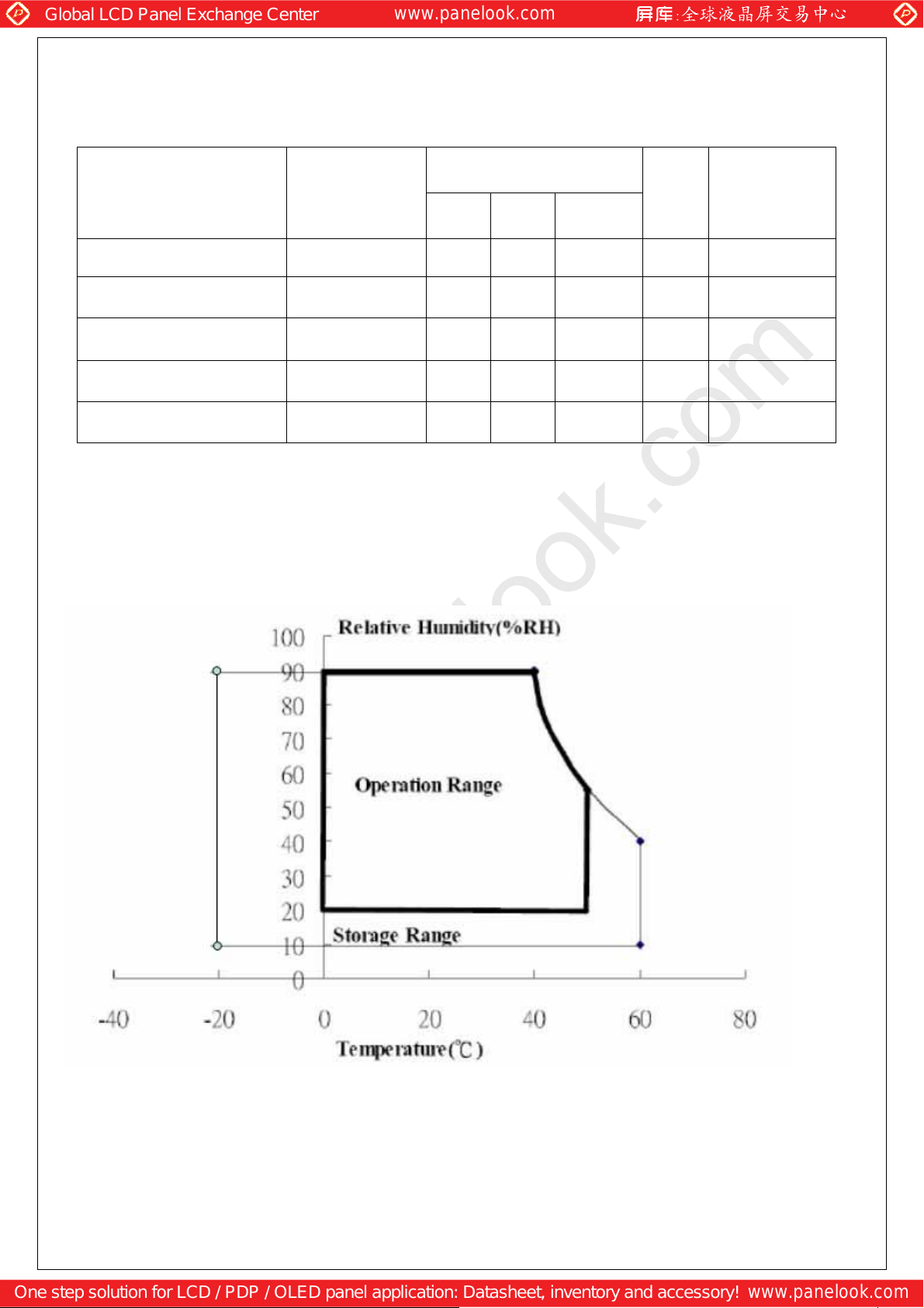
Note 1: The relative humidity must not exceed 90% non-condensing at temperatures of 40°C or less.
At temperatures greater than 40°C, the wet bulb temperature must not exceed 39°C.
-0.3 -
-0.3 -
0 -
-20 -
Values
Typ .
SPEC NO.
PAGE
Max.
6.0 V At 25°C
4.3 V At 25°C
50 °C Note 1
60 °C Note 2
MT200LW01 V.A
8/24
Unit
Remark
Note 2: The unit should not be exposed to corrosive chemicals.
Page 9

Global LCD Panel Exchange Center
www.panelook.com
One step solution for LCD / PDP / OLED panel application: Datasheet, inventory and accessory!
www.panelook.com
3. Electrical characteristics
a. Typical operating conditions
Item Symbol Min. Typ. Max. Unit Remark
Input Voltage
Permissive Power Input Ripple
Input Current
Rush Current
Logic Input
Voltage
LVD S:
IN+, IN-
Common Mode Voltage
Differential Input Voltage
Threshold Voltage (High)
Threshold Voltage (Low)
Black
White
Mosaic
SPEC NO.
PAGE
V
4.5 5 5.5
cc
V
- -
RF
MT200LW01 V.A
9/24
0.15
Icc - 800 1200
Icc - 600 900
I
- 750 1100
cc
I
- 1.6 3
Rush
mA
VCM - 1.2 -
VID 100 - 600
VTH - - 100
VTL -100 - -
mV
mV Note 5
mV Note 5
V
V
A Note 4
V
Note 1
Note 2
Note 3
Note 1 : The specified current is under the Vcc =5V, 25 °C, fv=60Hz (frame frequency) condition
whereas black pattern is displayed.
Note 2 : The specified current is under the Vcc =5V, 25 °C, fv=60Hz (frame frequency) condition
whereas white pattern is displayed.
Note 3 : The specified current is under the Vcc =5V, 25 °C, fv=60Hz (frame frequency) condition
whereas mosaic pattern(black & white [8*6] ) is displayed.
White : 255 Gray
Black : 0 Gray
Page 10

Global LCD Panel Exchange Center
www.panelook.com
One step solution for LCD / PDP / OLED panel application: Datasheet, inventory and accessory!
www.panelook.com
Note 4 : test condition :‘
(1) V
(2) Pattern: Mosaic pattern
(3) Test circuit
= 5 V, V
DD
10%
rising time = 470 µs ± 10%
DD
90%
SPEC NO.
V
DD
PAGE
MT200LW01 V.A
10/24
Ton=470 μs ± 10%
5 V
R1
47K
M1
2SK1059
FUSE
VDD ( LCD INPUT)
C1
1uF
CONTROL SIGNAL
(HIGH to LOW)
12V
Note 5: LVDS signal definition
VIN+ = Positive differential DATA & CLK Input
VIN- = Negative differential DATA & CLK Input
VID = VIN+ – VIN- ,
C3
1uF
R3
47K
R2
1K
M2
2SK1399
C2
10000pF
∆VCM =|VCM
∆VID =|VID
VID+ =|VIH
VID- =|VIL
VCM = (VIN
VCM+ = (VIH
VCM- = (VIL
–VCM-|,
+
–VID-|,
+
–VIH-|,
+
–VIL-|,
+
+VIN-)/2,
+
+VIH-)/2,
+
+VIL-)/2,
+
Page 11

Global LCD Panel Exchange Center
www.panelook.com
One step solution for LCD / PDP / OLED panel application: Datasheet, inventory and accessory!
www.panelook.com
Note 6 : Power on sequence for LCD V
T1
Panel Power
Supply V
Interface
Signals
DC
90%
10%
90% 90%
T2
DD
Valid Interface Data
90%
90%
SPEC NO.
PAGE
90%
T6
T5
10%
MT200LW01 V.A
11/24
T7
10%
Backlight Power
Supply
T3 T4
Parameter Value Unit
Min Typ Max ms
T1 0.1 - 10 ms
T2 0 30 50 ms
T3 200 250 - ms
T4 100 250 - ms
T5 0 20 50 ms
T6 0.1 - 50 ms
T7 1000 - - ms
Page 12

Global LCD Panel Exchange Center
www.panelook.com
One step solution for LCD / PDP / OLED panel application: Datasheet, inventory and accessory!
www.panelook.com
SPEC NO.
PAGE
MT200LW01 V.A
12/24
b. Display color vs. input data signals
The brightness of each primary color (red, green and blue) is based on the 8-bit gray scale data input
for the color; the higher the binary input, the brighter the color. The table below provides a reference for
color versus data input.
Color
MSB LSB MSB LSB MSB LSB
R7 R6 R5 R4 R3 R2 R1 R0
Red Green Blue
Input color data
G7 G6 G5 G4 G3 G2 G1 G0
B7 B6 B5 B4 B3 B2 B1 B0
Basic
colors
Black
Red(255)
Green(255)
Blue(255)
Cyan
Magenta
Yellow
White
0
0
0
0
0
0
1
1
1
1
1
1
0
0
0
0
0
0
0
0
0
0
0
0
0
0
0
0
0
0
1
1
1
1
1
1
1
1
1
1
1
1
1
1
1
1
1
1
0
0
0
0
0
0
0
0
0
1
1
1
0
0
0
0
0
1
0
0
0
1
1
1
1
1
1
1
1
0
1
1
0
0
1
1
0
0
1
1
1
1
0
0
0
0
1
1
1
0
0
0
1
1
1
0
0
0
1
1
1
1
1
1
0
0
0
0
0
0
0
0
0
0
0
1
1
0
0
1
1
0
0
1
1
1
1
0
0
0
0
1
1
1
1
1
1
1
1
1
0
0
0
1
1
1
0
0
0
0
0
0
0
0
0
0
0
0
0
1
1
1
1
1
1
1
1
1
1
1
1
1
1
1
0
0
0
0
0
1
1
1
1
1
0
0
0
0
0
Red
Green
Red(000) dark
Red(001)
Red(002)
:
Red(253)
Red(254)
Red(255) bright
Green(000)dark
Green(001)
G
reen(002)
:
Green(253)
Green(254)
Green(255)
bright
0
0
0
0
0
0
0
0
0
0
0
0
0
0
0
0
:
:
:
:
1
1
1
1
1
1
1
1
1
1
1
1
1
1
1
0
0
0
0
0
0
0
0
0
0
0
0
0
0
0
:
:
:
:
0
0
0
0
0
0
0
0
0
0
0
0
0
0
0
0
0
0
0
1
0
:
:
0
1
1
1
1
1
0
0
0
0
0
0
:
:
0
0
0
0
0
0
0
0
0
0
0
1
0
0
0
0
0
0
0
0
0
0
0
:
:
:
:
:
:
:
1
0
0
0
0
0
0
0
0
0
0
0
1
0
0
0
0
0
0
0
0
0
0
0
0
0
0
0
0
:
:
:
1
1
0
1
1
0
1
1
0
0
0
0
0
0
0
0
:
:
1
1
1
1
1
1
1
1
1
0
0
0
0
:
0
0
0
0
0
0
:
1
1
1
0
0
0
0
0
0
0
:
:
:
:
0
0
0
0
0
0
0
0
0
1
1
0
:
:
0
1
1
0
1
1
0
0
0
0
:
:
:
0
0
0
0
0
0
0
0
0
0
0
0
0
0
0
0
0
0
:
:
:
0
0
0
0
0
0
0
0
0
0
0
0
0
0
0
0
0
0
0
0
0
0
:
:
:
:
:
0
0
0
0
0
0
0
0
0
0
0
0
0
0
0
0
0
0
0
0
0
0
0
0
0
0
0
0
0
0
:
:
:
:
:
0
0
0
0
0
0
0
0
0
0
0
0
0
0
0
0
Blue(000) dark
Blue(001)
Blue(002)
Blue
Blue(253)
Blue(254)
Blue(255) bright
0
0
0
0
0
0
0
0
0
0
0
0
0
0
0
:
:
:
:
:
0
0
0
0
0
0
0
0
0
0
0
0
0
0
0
0
0
0
0
0
0
:
:
0
0
0
0
0
0
0
0
0
0
0
0
0
0
:
:
:
:
0
0
0
0
0
0
0
0
0
0
0
0
0
0
0
0
0
0
:
:
0
0
0
0
0
0
0
0
0
0
0
0
0
:
0
0
0
0
0
0
0
0
0
0
0
0
0
0
0
0
0
0
0
0
0
1
0
0
0
0
0
0
0
0
:
:
:
:
:
:
:
:
0
0
1
1
1
1
1
1
0
0
1
1
1
1
1
1
0
0
1
1
1
1
1
1
0
1
:
:
:
1
0
0
1
1
1
Page 13

Global LCD Panel Exchange Center
www.panelook.com
One step solution for LCD / PDP / OLED panel application: Datasheet, inventory and accessory!
www.panelook.com
SPEC NO.
PAGE
MT200LW01 V.A
13/24
c. Input signal timing
Support Input Timing Table
Item Description Min. Typ. Max. Unit
period 20.6 16.8 13.1 nS Clock
Dclk
frequency 48.5 59.5 76.1 MHz
Vertical
Horizontal
T
T
T
H_TOTAL
T
V total line number 905 926 942 T
V_TOTAL
Data duration
V_DATA
-
900
-
TVB V-blank 5 26 42 T
frequency 50 60 75 Hz
f
V
H_TOTAL
T
H_TOTAL
H_TOTAL
H total pixel number 950 1056 1150 DClk
Data duration
H_DATA
H-blank 150 256 350 DClk
T
HB
-
800
-
DClk
Note: Because this module is operated by DE only mode, Hsync and Vsync input signals should be set
to low Logic level or ground. Otherwise, this module would operate abnormally.
INPUT SIGNAL TIMING DIAGRAM
Tv
Tvd Tvb
DE
DCLK
Tc
Thb Thd
DE
DATA
Page 14

Global LCD Panel Exchange Center
www.panelook.com
One step solution for LCD / PDP / OLED panel application: Datasheet, inventory and accessory!
www.panelook.com
SPEC NO.
PAGE
MT200LW01 V.A
14/24
d. Display Position
D(1, 1) D(2, 1) …… D(720, 1) …… D(1599, 1) D(1600, 1)
D(1, 2) D(2, 2) …… D(720, 2) …… D(1599, 2) D(1600, 2)
.
.
.
D(1, 450) D(2, 450) …… D(720, 450) …… D(1599, 450) D(1600, 450)
.
.
.
D(1, 899) D(2, 899) …… D(720, 899) …… D(1599, 899) D(1600, 899)
D(1, 900) D(2, 900) …… D(720, 900) …… D(1599, 900) D(1600, 900)
……
……
.
.
.
.
.
.
……
……
.
.
.
.
.
.
e. Backlight driving conditions
Parameter Symbol Min. Typ. Max. Unit Remark Remark
Lamp voltage VL 711 790 869 Vrms I=7.5mA Note 1
Lamp operation current
IL 2.0 7.5 8.0 mArms Note 2
.
.
.
.
.
.
Lamp starting voltage VLstart
Frequency F 40
Lamp life time 50000 - - Hr Note 7
1650 - - T = 25°C Note 3,4,5,6
1800 - -
- 60
Vrms
T = 0°C Note 3,4,5,6
KHZ Note 6
Note: The waveform of the voltage output of inverter must be area-symmetric and the design of the
inverter must have specifications for the modularized lamp. The performance of the Backlight,
such as lifetime or brightness, is greatly influenced by the characteristics of the DC-AC inverter
for the lamp. All the parameters of an inverter should be carefully designed to avoid producing
too much current leakage from high voltage output of the inverter. When designing or ordering
the inverter please make sure that a poor lighting caused by the mismatch of the Backlight and
the inverter (miss-lighting, flicker, etc.) never occurs. If the above situation is confirmed, the
module should be operated in the same manners when it is installed in your instrument.
Note 1: Lamp voltage is specified under
IL = 7.5 mArms.
Note 2: The degree of unbalance: less than 10%
The ratio of wave height: less than
10%2 ±
Ip
Ip: high side peak
I-p
I-p: low side peak
The degree of unbalance = |Ip-I-p| /Irms*100(%)
The ratio of wave height = Ip (or I-p)/Irms
Lamp should be completely turned on.
Page 15

Global LCD Panel Exchange Center
www.panelook.com
One step solution for LCD / PDP / OLED panel application: Datasheet, inventory and accessory!
www.panelook.com
Note 3: Test equipment: AS-114B
Note 4: The voltage shown above should be applied to the lamp for more than 1 second after startup.
Otherwise, the lamp may not be turned on normally.
Note 5: Inverter should provide more than min. value, and then lamp could be completely turned on
Note 6: Lamp frequency may produce interference with horizontal synchronous frequency and this may
cause line flow on the display. Therefore lamp frequency shall be detached from the horizontal
synchronous frequency and its harmonics as far as possible in order to avoid interference.
Note 7: Life time (Hr) is defined as the time when brightness of a lamp unit itself becomes 50% or less
SPEC NO.
PAGE
MT200LW01 V.A
15/24
than its original value at the condition of Ta = 25±2°C and IL = 7.5 mArms.
Backlight connecter: 3500IHS-02L
Pin no. Symbol Function Remark
1 VIH Lamp high voltage input Cable color: Pink
2 VIL Lamp low voltage input Cable color: White
3 VIH Lamp high voltage input Cable color: Blue
4 VIL Lamp low voltage input Cable color: Black
Page 16

Global LCD Panel Exchange Center
www.panelook.com
One step solution for LCD / PDP / OLED panel application: Datasheet, inventory and accessory!
www.panelook.com
yp
C. Optical specifications
Item Symbol Condition
Response time
Tr+Tf
Contrast ratio
Viewing angle
CR
Top
Bottom
Tr
Tf
θ= 0∘
θ= 0∘
CR≧10
CR≧10
SPEC NO.
PAGE
Specification
Min. T
- 1.5 4
- 3.5 6
- 5 10
700 1000 -
70 80 -
70 80 -
.Max.
MT200LW01 V.A
16/24
Unit Remark
ms Note 4
Note 3,5
deg. Note 3,5,7
Left
Right
Brightness (Center)
Wx
Color chromaticity(CIE)
Wy
White uniformity (9) δW
Cross talk Ct
YL
Rx
Ry
Gx
Gy
Bx
By
CR≧10
CR≧10
θ= 0∘
75 85 -
75 85 -
200 250 -
0.313
0.329
0.648
-0.03
0.75 0.80 -
- - 2%
0.336
0.294
0.607
0.145
0.064
+0.03
nit Note 3,6
Note 3
Note 3,8
Note 9
Note 1: Ambient temperature = 25°C.
Note 2: To be measured in dark room after backlight warm up 30 minutes.
Note 3: To be measured with a viewing cone of 2°by Topcon luminance meter BM-5A.
Note 4: Definition of response time:
The output signals of BM-7 are measured when the input signals are changed from “Black”
to “White” (falling time) and from “White” to “Black” (rising time), respectively. The response time
interval is between the 10% and 90% of amplitudes. Refer to figure as below.
Page 17

Global LCD Panel Exchange Center
www.panelook.com
One step solution for LCD / PDP / OLED panel application: Datasheet, inventory and accessory!
www.panelook.com
)
100%
S
ig
90%
n
a
l(
R
e
la
t
iv
e
v
a
lu
10%
e
)
0%
Note 5: Definition of contrast ratio:
Contrast ratio is calculated by the following formula.
Contrast ratio (CR
"Black"
Tr
Brightness on the "white" state
=
Brightness on the "black" state
SPEC NO.
PAGE
Tf
MT200LW01 V.A
17/24
"White""White"
Note 6: Driving conditions for CCFL: I
Note 7: Definition of viewing angle
Note 8: Definition white uniformity:
Luminance are measured at the following nine points (P1~P9).
δ
Minimum Brightness of nine points(P1~P9).
=
Maximum Brightness of nine points (P1~P9).
= 7.5 mA, 50 KHz Frequency.
L
Page 18

Global LCD Panel Exchange Center
www.panelook.com
One step solution for LCD / PDP / OLED panel application: Datasheet, inventory and accessory!
www.panelook.com
Note 9:
SPEC NO.
1/2
1/6
PAGE
2/3 1/3
A
1/6
A’
127 gray level 127 gray level
B
1/2
1/2
MT200LW01 V.A
18/24
1/6
1/6
1/3
1/2
B’
2/3
l L
l L
l / LA x 100%= 2% max., LA and LA’ are brightness at location A and A’
A-LA’
l / LB x 100%= 2% max., LB and LB’ are brightness at location B and B’
B-LB’
Note 10: Optical characteristic measurement setup.
0 gray level
Page 19

Global LCD Panel Exchange Center
www.panelook.com
One step solution for LCD / PDP / OLED panel application: Datasheet, inventory and accessory!
www.panelook.com
D. Reliability test items
Test Item Test Condition Judgment Remark
High temperature & high
humidity operation
High temperature operation
Low temperature operation
Thermal Shock
(non-operation)
Electrostatic discharge (ESD)
SPEC NO.
40°C, 90%RH, 240Hrs
(No condensation)
50°C, 240Hrs
0°C, 240Hrs
-20°C~60°C
1Hr, 1Hr, 100cycles
Contact:+/-8kV, 150pF(330ohms), 16 points,
10 times/1 point, 1 time/1 sec
Air discharge:+/-15kV, 150pF(330ohms),
9points, 10 times/1 point, 1 time/1 sec
PAGE
MT200LW01 V.A
19/24
Note 1 Note 2
Note 1 Note 2
Note 1 Note 2
Note 1 Note 2
Note 1 Note 2
Vibration
(non-operation)
Mechanical Shock
(non-operation)
MTBF Demonstration 50,000 hours (Min.) with confidence level 90% Note 1 Note 3
Vibration level : 1.5G
Bandwidth : 10-300Hz
Waveform : sine wave,
sweep rate : 10min
30 min for each direction X, Y, Z
(1.5 Hrs in total)
Shock level : 50G, 11ms
Waveform : Half sine wave
Direction : ±X, ±Y, ±Z
One time each direction
Note 1 Note 2
Note 1 Note 2
Note1: Pass: Normal display image with no obvious non-uniformity and no line defect.
Partial transformation of the module parts should be ignored.
Fail: No display image, obvious non-uniformity, or line defects.
Note2: Evaluation should be tested after storage at room temperature for one hour.
Note 3: The MTBF calculation is based on the assumption that the failure rate distribution meets the
Exponential Model (CCFL excluded)
Page 20

Global LCD Panel Exchange Center
www.panelook.com
One step solution for LCD / PDP / OLED panel application: Datasheet, inventory and accessory!
www.panelook.com
SPEC NO.
PAGE
MT200LW01 V.A
20/24
E. Safety
(1) Sharp Edge Requirements
There will be no sharp edges or corners on the display assembly that could cause injury.
(2) Materials
a. Toxicity
There will be no carcinogenic materials used anywhere in the display module. If toxic materials
are used, they will be reviewed and approved by the responsible InnoLux Toxicologist.
b. Flammability
All components including electrical components that do not meet the flammability grade UL94-V1
in the module will complete the flammability rating exception approval process. The printed circuit
board will be made from material rated 94-V1 or better. The actual UL flammability rating will be
printed on the printed circuit board.
c. Capacitors
If any polarized capacitors are used in the display assembly, provisions will be made to keep them
from being inserted backwards.
F. Display quality
The display quality of the color TFT-LCD module should be in compliance with the
Innolux’s Incoming inspection standard.
G. Handling precaution
The Handling of the TFT-LCD should be in compliance with the Innolux’s handling principle
standard.
Page 21

Global LCD Panel Exchange Center
www.panelook.com
One step solution for LCD / PDP / OLED panel application: Datasheet, inventory and accessory!
www.panelook.com
m
H. Label
(1) Module Label
18 mm
(a) Model Number: MT200LW01
(b) Version: V.A
MT200LW01 V.A AM2000001 0xx
Z1 Z2 Z3 Z4 Z
Z1 'Z2'-Z3' Z4'Z 5'Z 6'Z7'-Z8' - Z9 '- Z10 '- Z11' Z12'-Z13'-Z14' Z15' -Z16 '-Z17 'Z18' Z19' -Z20'Z21'Z22 ' Z
--Z 7--Z8 Z9 Z10 Z
5 Z 6
73 m
11 Z 12
SPEC NO.
PAGE
MT200LW01 V.A
21/24
'
23
MADE IN XXX
(c) Serial ID I: Z
Z2 Z3 Z4 Z 5 Z
1
Z
6
7
Serial ID includes the information as below:
1. Manufactured Date: Year: 0~9, for 2000~2009
2. Month: 1~9 & A~C for Jan.~Dec.
3. Date: 1~9 & A~Z (exclude I, O, Q, U) for 1st~31th
4. Code of grade: 1, 2, 3, 5, E
Z8 Z
9 Z10
Z
Z
12
11
Serial No
Code of grade
INL internal use
INL internal use
Year, Month, Date
INL internal use
5. Serial No: Module manufacture sequence no
(d) Serial ID II (INL internal use)
Page 22

Global LCD Panel Exchange Center
www.panelook.com
One step solution for LCD / PDP / OLED panel application: Datasheet, inventory and accessory!
www.panelook.com
(2) Carton Label
INNOLUX DISPLAY
BOX ID :
60 mm
Model No. MT200LW01 V.A
AM2000001 0XX
Quantity : 7 PCS
MFG Date: 20XX/XX/XX
QC: Made in XXX
Z1 Z2 Z3 Z4 --Z 5--Z6 Z7 Z8 Z 9
SPEC NO.
PAGE
MT200LW01 V.A
22/24
100 mm
(a) Model Number: MT200LW01
(b) Version: V.A
(c) Packing quantity: 7 pcs
(d) Serial ID: Z
Z2 Z3 Z4 Z 5 Z6 Z
1
7 Z8
Z 9
Serial No
Code of grade
Serial ID includes the information as below:
(a) Manufactured Date: Year: 0~9, for 2000~2009
Month: 1~9 & A~C for Jan.~Dec.
Date: 1~9 & A~Z (exclude I, O, Q, U) for 1st~31th
Year, Month, Date
INL internal use
(b) Code of grade: 1,2, 3, 5, E
(c) Serial No: Module packing sequence no
Page 23

Global LCD Panel Exchange Center
www.panelook.com
One step solution for LCD / PDP / OLED panel application: Datasheet, inventory and accessory!
www.panelook.com
SPEC NO.
PAGE
MT200LW01 V.A
23/24
Page 24

Global LCD Panel Exchange Center
www.panelook.com
One step solution for LCD / PDP / OLED panel application: Datasheet, inventory and accessory!
www.panelook.com
SPEC NO.
PAGE
MT200LW01 V.A
24/24
 Loading...