


Global LCD Panel Exchange Center |
www.panelook.com |
PRODUCT SPECIFICATION
Doc. Number :
Tentative Specification
Preliminary Specification
Approval Specification
MODEL NO.: M215HGE
SUFFIX: P01
Customer: |
|
APPROVED BY |
SIGNATURE |
Name / Title |
|
Note |
|
Product Version C1/C2 |
|
Please return 1 copy for your confirmation with your |
|
signature and comments. |
|
Approved By |
Checked By |
Prepared By |
Version 2.0 |
8 March 2011 |
1 / 25 |
|
|
|
The copyright belongs to CHIMEI InnoLux. Any unauthorized use is prohibited.
One step solution for LCD / PDP / OLED panel application: Datasheet, inventory and accessory! www.panelook.com

Global LCD Panel Exchange Center |
www.panelook.com |
PRODUCT SPECIFICATION
- CONTENTS - |
|
1. GENERAL DESCRIPTION....................................................................................................................... |
4 |
1.1 OVERVIEW........................................................................................................................................ |
4 |
1.2 GENERAL SPECIFICATI0NS........................................................................................................... |
4 |
2. MECHANICAL SPECIFICATIONS .......................................................................................................... |
4 |
3. ABSOLUTE MAXIMUM RATINGS .......................................................................................................... |
5 |
3.1 ABSOLUTE RATINGS OF ENVIRONMENT.................................................................................. |
5 |
3.2 ELECTRICAL ABSOLUTE RATINGS ............................................................................................. |
5 |
3.2.1 TFT LCD MODULE .............................................................................................................. |
5 |
3.3 ABSOLUTE RATINGS OF ENVIRONMENT (OPEN CELL)......................................................... |
5 |
4. ELECTRICAL SPECIFICATIONS.............................................................................................................. |
6 |
4.1 FUNCTION BLOCK DIAGRAM...................................................................................................... |
6 |
4.2. INTERFACE CONNECTIONS......................................................................................................... |
6 |
4.3 ELECTRICAL CHARACTERISTICS ............................................................................................... |
8 |
4.4 Vcc POWER DIP CONDITION ....................................................................................................... |
10 |
4.5 LVDS DATA MAPPING TABLE ..................................................................................................... |
10 |
4.6 COLOR DATA INPUT ASSIGNMENT........................................................................................... |
11 |
4.7 DISPLAY TIMING SPECIFICATIONS........................................................................................... |
12 |
4.8 POWER ON/OFF SEQUENCE........................................................................................................ |
14 |
5. OPTICAL CHARACTERISTICS............................................................................................................. |
15 |
5.1 TEST CONDITIONS ........................................................................................................................ |
15 |
5.2 OPTICAL SPECIFICATIONS.......................................................................................................... |
15 |
5.3 Flicker Adjustment ............................................................................................................................ |
18 |
6. RELIABILITY TEST ITEM....................................................................................................................... |
20 |
7. LABEL........................................................................................................................................................ |
21 |
7.1 CMI OPEN CELL LABEL ............................................................................................................... |
21 |
7.2 CARTON LABEL............................................................................................................................. |
21 |
8. PACKING ................................................................................................................................................... |
22 |
8.1 Packing Information.......................................................................................................................... |
22 |
8.2 CARTON........................................................................................................................................... |
22 |
8.3 PALLET ............................................................................................................................................ |
23 |
9. PRECAUTIONS........................................................................................................................................ |
24 |
9.1 HANDLING PRECAUTIONS ......................................................................................................... |
24 |
9.2 SAFETY PRECAUTIONS ............................................................................................................... |
24 |
9.3 OTHER.............................................................................................................................................. |
24 |
10. OUTLINE DRAWING............................................................................................................................. |
24 |
Version 2.0 |
8 March 2011 |
2 / 25 |
|
|
|
The copyright belongs to CHIMEI InnoLux. Any unauthorized use is prohibited.
One step solution for LCD / PDP / OLED panel application: Datasheet, inventory and accessory! www.panelook.com
Global LCD Panel Exchange Center |
www.panelook.com |
PRODUCT SPECIFICATION
REVISION HISTORY
Version |
Date |
Page |
Description |
|
|
|
|
2.0 |
Mar.08, 2011 |
All |
Spec Ver.2.0 was first issued. |
|
|
|
|
Version 2.0 |
8 March 2011 |
3 / 25 |
|
|
|
The copyright belongs to CHIMEI InnoLux. Any unauthorized use is prohibited.
One step solution for LCD / PDP / OLED panel application: Datasheet, inventory and accessory! www.panelook.com
Global LCD Panel Exchange Center |
www.panelook.com |
PRODUCT SPECIFICATION
1. GENERAL DESCRIPTION
1.1 OVERVIEW
The M215HGE-P01 is a 21.5” TFT LCD cell with driver ICs and a 30-pins-2ch-LVDS circuit board.
The product supports 1920 x 1080 WXGA mode and can display up to 16.7M colors. The backlight unit
is not built in.
1.2 GENERAL SPECIFICATI0NS
Item |
Specification |
Unit |
Note |
Screen Size |
21.5 real diagonal |
|
|
Driver Element |
a-si TFT active matrix |
- |
- |
Pixel Number |
1920 x R.G.B. x 1080 |
pixel |
- |
Pixel Pitch |
0.2482 (H) x 0.2482 (V) |
mm |
- |
Pixel Arrangement |
RGB vertical stripe |
- |
- |
Display Colors |
16.7M |
color |
- |
Transmissive Mode |
Normally white |
- |
- |
Surface Treatment |
AG type, 3H hard coating, Haze 25 |
- |
- |
Power Consumption |
6.3 |
Watt |
- |
2. MECHANICAL SPECIFICATIONS
Item |
Min. |
Typ. |
Max. |
Unit |
Note |
|
Weight |
- |
554.2 |
574.2 |
g |
- |
|
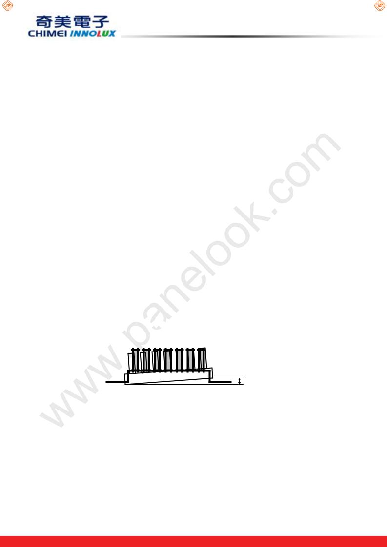
I/F connector mounting |
The mounting |
inclination of the |
connector makes |
- |
(2) |
|
position |
the screen center within ±0.5mm as the horizontal. |
|||||
|
|
|||||
Note (1) Please refer to the attached drawings for more information of front and back outline dimensions.
(2)Connector mounting position


(3)Please refer to sec.3.1 for more information of power consumption.
+/- 0.5mm
Version 2.0 |
8 March 2011 |
4 / 25 |
|
|
|
The copyright belongs to CHIMEI InnoLux. Any unauthorized use is prohibited.
One step solution for LCD / PDP / OLED panel application: Datasheet, inventory and accessory! www.panelook.com
Global LCD Panel Exchange Center |
www.panelook.com |
PRODUCT SPECIFICATION
3.ABSOLUTE MAXIMUM RATINGS
3.1ABSOLUTE RATINGS OF ENVIRONMENT
Item |
Symbol |
|
Value |
Unit |
Note |
|
Min. |
|
Max. |
||||
|
|
|
|
|
||
Storage Temperature |
TST |
-20 |
|
+60 |
ºC |
(1) |
Operating Ambient Temperature |
TOP |
0 |
|
+50 |
ºC |
(1), (2) |
Note (1) (a) 90 %RH Max. (Ta <= 40 ºC).
(b) Wet-bulb temperature should be 39 ºC Max. (Ta > 40 ºC).
(c) No condensation.
Note (2) The temperature of panel surface should be 0 ºC min. and 60 ºC max.
Relative Humidity (%RH)
|
|
100 |
|
|
|
|
|
|
90 |
|
|
|
|
|
|
80 |
|
|
|
|
|
|
60 |
Operating Range |
|
|
|
|
|
|
|
|
|
|
|
|
40 |
|
|
|
|
|
|
20 |
Storage Range |
|
|
|
|
|
10 |
|
|
||
-40 |
-20 |
0 |
20 |
40 |
60 |
80 |
Temperature (ºC)
3.2 ELECTRICAL ABSOLUTE RATINGS

3.2.1 TFT LCD MODULE
Item |
Symbol |
|
Value |
Unit |
Note |
|
Min |
|
Max |
||||
|
|
|
|
|
||
Power Supply Voltage |
VCC |
-0.3 |
|
+6.0 |
V |
(1) |
Note (1) Permanent damage to the device may occur if maximum values are exceeded. Function operation should be restricted to the conditions described under Normal Operating Conditions.
3.3ABSOLUTE RATINGS OF ENVIRONMENT (OPEN CELL)
High temperature or humidity may reduce the performance of panel. Please store LCD panel within the
 specified storage conditions.
Storage Condition: With packing.
Storage temperature range: 25±5 ºC.
Storage humidity range: 50±10%RH.
Shelf life: 30days
Version 2.0 |
8 March 2011 |
5 / 25 |
|
|
|
The copyright belongs to CHIMEI InnoLux. Any unauthorized use is prohibited.
One step solution for LCD / PDP / OLED panel application: Datasheet, inventory and accessory! www.panelook.com

Global LCD Panel Exchange Center |
www.panelook.com |
PRODUCT SPECIFICATION
4.ELECTRICAL SPECIFICATIONS
4.1 FUNCTION BLOCK DIAGRAM
4.2. INTERFACE CONNECTIONS
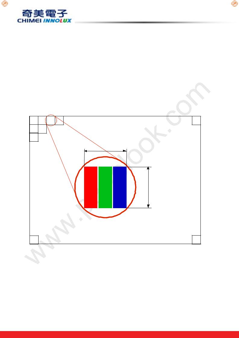
PIN ASSIGNMENT
|
Pin |
Name |
Description |
|
|
|
1 |
RXO0- |
Negative LVDS differential data input. Channel O0 (odd) |
|
|
|
2 |
RXO0+ |
Positive LVDS differential data input. Channel O0 (odd) |
|
|
|
3 |
RXO1- |
Negative LVDS differential data input. Channel O1 (odd) |
|
|
|
4 |
RXO1+ |
Positive LVDS differential data input. Channel O1 (odd) |
|
|
|
5 |
RXO2- |
Negative LVDS differential data input. Channel O2 (odd) |
|
|
|
6 |
RXO2+ |
Positive LVDS differential data input. Channel O2 (odd) |
|
|
|
7 |
GND |
Ground |
|
|
|
8 |
RXOC- |
Negative LVDS differential clock input. (odd) |
|
|
|
9 |
RXOC+ |
Positive LVDS differential clock input. (odd) |
|
|
|
10 |
RXO3- |
Negative LVDS differential data input. Channel O3(odd) |
|
|
|
11 |
RXO3+ |
Positive LVDS differential data input. Channel O3 (odd) |
|
|
|
12 |
RXE0- |
Negative LVDS differential data input. Channel E0 (even) |
|
|
|
13 |
RXE0+ |
Positive LVDS differential data input. Channel E0 (even) |
|
|
|
14 |
GND |
Ground |
|
|
|
15 |
RXE1- |
Negative LVDS differential data input. Channel E1 (even) |
|
|
|
16 |
RXE1+ |
Positive LVDS differential data input. Channel E1 (even) |
|
|
|
17 |
GND |
Ground |
|
|
|
18 |
RXE2- |
Negative LVDS differential data input. Channel E2 (even) |
|
|
|
19 |
RXE2+ |
Positive LVDS differential data input. Channel E2 (even) |
|
|
|
20 |
RXEC- |
Negative LVDS differential clock input. (even) |
|
|
|
21 |
RXEC+ |
Positive LVDS differential clock input. (even) |
|
|
|
22 |
RXE3- |
Negative LVDS differential data input. Channel E3 (even) |
|
|
|
23 |
RXE3+ |
Positive LVDS differential data input. Channel E3 (even) |
|
|
|
24 |
GND |
Ground |
|
|
|
25 |
NC |
For LCD internal use only, Do not connect |
|
|
|
|
|
|
|
|
Version 2.0 |
|
8 March 2011 |
6 / 25 |
||
|
|
|
|
|
|
The copyright belongs to CHIMEI InnoLux. Any unauthorized use is prohibited.
One step solution for LCD / PDP / OLED panel application: Datasheet, inventory and accessory! www.panelook.com
Global LCD Panel Exchange Center |
www.panelook.com |
PRODUCT SPECIFICATION
26 |
|
NC |
|
For LCD internal use only, Do not connect |
27 |
|
NC |
|
For LCD internal use only, Do not connect |
28 |
|
Vcc |
|
+5.0V power supply |
29 |
|
Vcc |
|
+5.0V power supply |
30 |
|
Vcc |
|
+5.0V power supply |
Note |
(1) |
Connector Part No.: |
|
|
|
|
093G30-B0001A(STARCONN) or MSAKT2407P30HA(STM) or equivalent |
||
Note |
(2) |
User’s connector Part No: |
|
|
|
|
Mating Wire Cable Connector Part No.: FI-X30H(JAE) or FI-X30HL(JAE) |
||
|
|
Mating FFC Cable Connector Part No.: 217007-013001 (P-TWO) or JF05X030-1 (JAE). |
||
Note |
(3) |
The first pixel is odd. |
|
|
Note |
(4) |
Input signal of even and odd clock should be the same timing. |
||
1,1 1,2 1,3 1,4 |
1,Xmax |
|
(odd) |
(even) (odd) (even) |
|
2,1 |
2,2 |
|
3,1 |
|
|
|
|
Pitch |
|
|
Pitch |
Ymax,1 |
|
Ymax, |
|
Xmax |
|
|
|
|
Version 2.0 |
8 March 2011 |
7 / 25 |
|
|
|
The copyright belongs to CHIMEI InnoLux. Any unauthorized use is prohibited.
One step solution for LCD / PDP / OLED panel application: Datasheet, inventory and accessory! www.panelook.com
Global LCD Panel Exchange Center |
www.panelook.com |
PRODUCT SPECIFICATION
4.3 ELECTRICAL CHARACTERISTICS
Parameter |
Symbol |
Value |
Unit |
Note |
|
Typ. |
|||||
|
Min. |
Max. |
|
Power Supply Voltage |
Vcc |
4.5 |
5.0 |
5.5 |
V |
- |
||
Ripple Voltage |
|
VRP |
-- |
-- |
300 |
mV |
- |
|
Rush Current |
|
IRUSH |
-- |
-- |
3 |
A |
(2) |
|
|
|
White |
- |
-- |
0.51 |
0.61 |
A |
(3)a |
Power Supply Current |
|
Black |
- |
-- |
1.05 |
1.26 |
A |
(3)b |
|
Vertical Stripe |
- |
-- |
1.06 |
1.26 |
A |
(3)c |
|
Power Consumption |
PLCD |
- |
5.3 |
6.3 |
Watt |
(4) |
||
LVDS differential input voltage |
Vid |
200 |
- |
600 |
mV |
|
||
LVDS common input voltage |
Vic |
1 |
1.2 |
1.4 |
V |
|
||


 Ta = 25 ± 2 ºC Note (1) The ambient temperature is Ta = 25 ± 2 ºC.


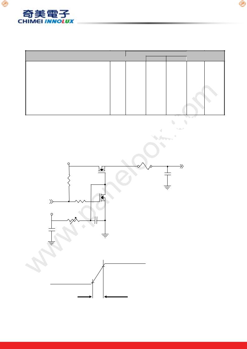
Note (2) IRUSH: the maximum current when VCCS is rising 


 IIS: the maximum current of the first 100ms after power-on


Measurement Conditions: Shown as the following figure. Test pattern: black.
+5.0V |
|
|
|
|
|
|
Q1 |
2SK1475 |
|
|
|
|
|
Vcc |
|
|
|
FUSE |
C3 |
|
|
|
(LCD Module Input) |
|
R1 |
|
|
|
1uF |
47K |
|
|
|
|
(High to Low) |
|
|
|
|
(Control Signal) |
|
|
Q2 |
|
|
R2 |
|
|
|
|
|
|
|
|
SW |
|
|
2SK1470 |
|
|
1K |
|
|
|
+12V |
|
|
|
|
VR1 |
47K |
C2 |
|
|
C1 |
|
0.01uF |
|
|
|
|
|
|
|
1uF |
|
|
|
|
Vcc rising time is 470μs
Vcc
0.9Vcc
0.1Vcc
GND
470μs
Note (3) The specified power supply current is under the conditions at Vcc = 5.0 V, Ta = 25 ± 2 ºC, Fv = 60 Hz, whereas a power dissipation check pattern below is displayed.
Version 2.0 |
8 March 2011 |
8 / 25 |
|
|
|
The copyright belongs to CHIMEI InnoLux. Any unauthorized use is prohibited.
One step solution for LCD / PDP / OLED panel application: Datasheet, inventory and accessory! www.panelook.com
 Loading...