

Page 1
PRODUCT SPECIFICATION
Doc. Number :
■ Tentative Specification
□ Preliminary Specification
□ Approval Specification
MODEL NO.: M195FGE
SUFFIX: P03
Customer:
APPROVED BY SIGNATURE
Name / Title
Note
Product Version C1
Please return 1 copy for your confirmation with your signature and
comments.
Approved By Checked By Prepared By
吳柏勳
吳柏勳
吳柏勳吳柏勳
Version 0.0 9 January 2013 1 / 26
The copyright belongs to InnoLux. Any unauthorized use is prohibited.
陳
陳立
陳陳
立錚
錚
立立
錚錚
林燕輝
林燕輝
林燕輝林燕輝
Page 2

PRODUCT SPECIFICATION
- CONTENTS -
1. GENERAL DESCRIPTION......................................................................................................4
1.1 OVERVIEW .......................................................................................................................4
1.2 GENERAL SPECIFICATI0NS............................................................................................4
2. MECHANICAL SPECIFICATIONS ..........................................................................................4
3. ABSOLUTE MAXIMUM RATINGS ..........................................................................................4
3.1 ABSOLUTE RATINGS OF ENVIRONMENT......................................................................4
3.2 ELECTRICAL ABSOLUTE RATINGS................................................................................5
3.2.1 TFT LCD MODULE.................................................................................................... 5
3.3 ABSOLUTE RATINGS OF ENVIRONMENT (OPEN CELL) ..............................................5
4. ELECTRICAL SPECIFICATIONS............................................................................................6
4.1 FUNCTION BLOCK DIAGRAM .........................................................................................6
4.2. INTERFACE CONNECTIONS..........................................................................................6
Connector Information.............................................................................................................7
4.3 ELECTRICAL CHARACTERISTICS..................................................................................8
4.4 Vcc POWER DIP CONDITION........................................................................................10
4.5 LVDS DATA MAPPING TABLE ........................................................................................10
4.6 COLOR DATA INPUT ASSIGNMENT.............................................................................. 11
4.7 DISPLAY TIMING SPECIFICATIONS..............................................................................12
4.8 POWER ON/OFF SEQUENCE........................................................................................14
5. OPTICAL CHARACTERISTICS ............................................................................................15
5.1 TEST CONDITIONS........................................................................................................15
5.2 OPTICAL SPECIFICATIONS...........................................................................................15
5.3 Flicker Adjustment...........................................................................................................18
6. RELIABILITY TEST ITEM .....................................................................................................19
7. LABEL...................................................................................................................................20
7.1 CMI OPEN CELL LABEL.................................................................................................20
8. PACKING...............................................................................................................................21
8.1 Packing Information.........................................................................................................21
8.2 CARTON..........................................................................................................................21
9. PRECAUTIONS.....................................................................................................................23
9.1 ASSEMBLY AND HANDLING PRECAUTIONS ...............................................................23
9.2 SAFETY PRECAUTIONS................................................................................................25
10. OUTLINE DRAWING...........................................................................................................26
Version 0.0 9 January 2013 2 / 26
The copyright belongs to InnoLux. Any unauthorized use is prohibited.
Page 3

PRODUCT SPECIFICATION
REVISION HISTORY
Version Date Page Description
0.0 Jan.2013 All Spec Ver.0.0 was first issued.
Version 0.0 9 January 2013 3 / 26
The copyright belongs to InnoLux. Any unauthorized use is prohibited.
Page 4
PRODUCT SPECIFICATION
1. GENERAL DESCRIPTION
1.1 OVERVIEW
The M195FGE-P03 is a 19.5” TFT LCD cell with driver ICs and a 30-pins-2ch-LVDS circuit board.
The product supports 1600 x 900 HD+ mode and can display up to 16.7M colors. The backlight unit
is not built in.
1.2 GENERAL SPECIFICATI0NS
Item Specification Unit Note
Screen Size 19.5” real diagonal
Driver Element a-si TFT active matrix - -
Pixel Number 1600 x R.G.B. x 900 pixel -
Pixel Pitch 0.27 (H) x 0.27 (V) mm -
Pixel Arrangement RGB vertical stripe - -
Display Colors 16.7M color -
Transmissive Mode Normally white - -
Surface Treatment AG type, 3H hard coating, Haze 25 - -
Power Consumption 4.55 (Max) Watt -
2. MECHANICAL SPECIFICATIONS
Item Min. Typ. Max. Unit Note
Weight
I/F connector mounting
position
Note (1) Please refer to the attached drawings for more information of front and back outline dimensions.
Note (2) Connector mounting position
Note (3) Please refer to sec.3.1 for more information of power consumption.
the screen center within ±0.5mm as the horizontal.
-
The mounting inclination of the connector makes
345 365 g -
- (2)
3. ABSOLUTE MAXIMUM RATINGS
3.1 ABSOLUTE RATINGS OF ENVIRONMENT
Item Symbol
Storage Temperature TST -20 +60 ºC (1)
Operating Ambient Temperature TOP 0 +50 ºC (1), (2)
Note (1) (a) 90 %RH Max. (Ta <= 40 ºC).
Min. Max.
Value
Unit Note
(b) Wet-bulb temperature should be 39 ºC Max. (Ta > 40 ºC).
(c) No condensation.
Version 0.0 9 January 2013 4 / 26
The copyright belongs to InnoLux. Any unauthorized use is prohibited.
Page 5
PRODUCT SPECIFICATION
Note (2) The temperature of panel surface should be 0 ºC min. and 60 ºC max.
3.2 ELECTRICAL ABSOLUTE RATINGS
3.2.1 TFT LCD MODULE
Item Symbol
Power Supply Voltage VCC -0.3 6.0 V (1)
Note (1) Permanent damage to the device may occur if maximum values are exceeded. Function operation
should be restricted to the conditions described under Normal Operating Conditions.
Value
Min Max
Unit Note
3.3 ABSOLUTE RATINGS OF ENVIRONMENT (OPEN CELL)
High temperature or humidity may reduce the performance of panel. Please store LCD panel within the
specified storage conditions.
Storage Condition: With packing.
Storage temperature range: 25±5 ºC.
Storage humidity range: 50±10%RH.
Shelf life: 30days
Version 0.0 9 January 2013 5 / 26
The copyright belongs to InnoLux. Any unauthorized use is prohibited.
Page 6
4. ELECTRICAL SPECIFICATIONS
4.1 FUNCTION BLOCK DIAGRAM
PRODUCT SPECIFICATION
4.2. INTERFACE CONNECTIONS
PIN ASSIGNMENT
Pin Name Description
1 RXO0- Negative LVDS differential data input. Channel O0 (odd)
2 RXO0+ Positive LVDS differential data input. Channel O0 (odd)
3 RXO1- Negative LVDS differential data input. Channel O1 (odd)
4 RXO1+ Positive LVDS differential data input. Channel O1 (odd)
5 RXO2- Negative LVDS differential data input. Channel O2 (odd)
6 RXO2+ Positive LVDS differential data input. Channel O2 (odd)
7 GND Ground
8 RXOC- Negative LVDS differential clock input. (odd)
9 RXOC+ Positive LVDS differential clock input. (odd)
10 RXO3- Negative LVDS differential data input. Channel O3(odd)
11 RXO3+ Positive LVDS differential data input. Channel O3 (odd)
12 RXE0- Negative LVDS differential data input. Channel E0 (even)
13 RXE0+ Positive LVDS differential data input. Channel E0 (even)
14 GND Ground
15 RXE1- Negative LVDS differential data input. Channel E1 (even)
16 RXE1+ Positive LVDS differential data input. Channel E1 (even)
17 GND Ground
18 RXE2- Negative LVDS differential data input. Channel E2 (even)
19 RXE2+ Positive LVDS differential data input. Channel E2 (even)
20 RXEC- Negative LVDS differential clock input. (even)
21 RXEC+ Positive LVDS differential clock input. (even)
22 RXE3- Negative LVDS differential data input. Channel E3 (even)
23 RXE3+ Positive LVDS differential data input. Channel E3 (even)
24 GND Ground
25 NC For LCD internal use only, Do not connect
26 NC For LCD internal use only, Do not connect
27 NC For LCD internal use only, Do not connect
Version 0.0 9 January 2013 6 / 26
The copyright belongs to InnoLux. Any unauthorized use is prohibited.
Page 7
PRODUCT SPECIFICATION
Pitch
28 Vcc +5.0V power supply
29 Vcc +5.0V power supply
30 Vcc +5.0V power supply
Connector Information
Item Description
Manufacturer FCN/ P-TWO/ Foxconn
Type part number FCN:WF13-423-3033
P-TWO:187098-30091
Foxconn:GS23302-0311R-7H
Mating housing part number FCN: FI-X30HL(JAE)
P-TWO: SE 1220HS-D(JAE)
Foxconn: FI-X30H(JAE)
*Notice: There would be compatible issues, if not using the indicated connectors in the
matching list.
Note (1) The first pixel is odd.
Note (2) Input signal of even and odd clock should be the same timing.
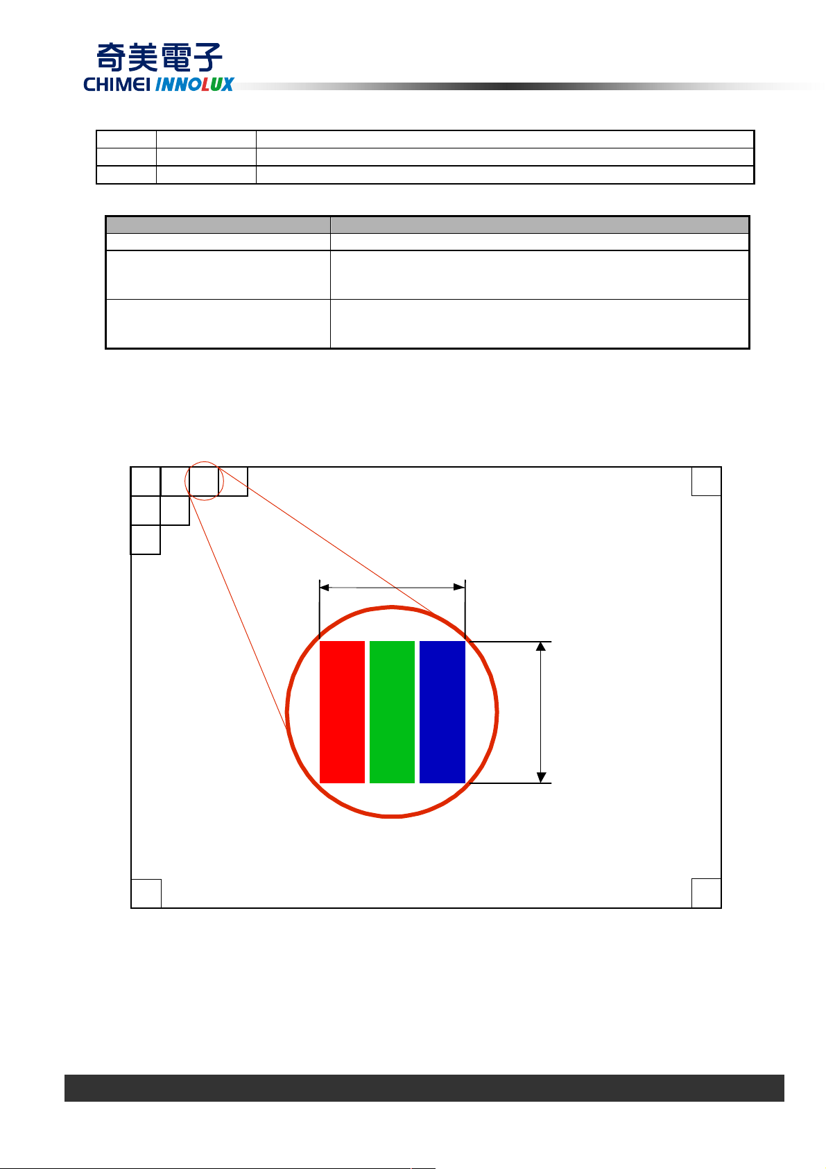
1,1
(odd)
2,1
3,1
1,2
(even)
2,2
1,3
(odd)
1,4
(even)
1,Xmax
Pitch
Ymax,1
Version 0.0 9 January 2013 7 / 26
The copyright belongs to InnoLux. Any unauthorized use is prohibited.
Ymax,
Xmax
Page 8
4.3 ELECTRICAL CHARACTERISTICS
Parameter Symbol
Power Supply Voltage Vcc 4.5 5 5.5 V -
Ripple Voltage VRP - - 300 mV -
Rush Current I
White 0.43 0.48 A (3)a
Power Supply Current
Power Consumption PLCD
LVDS differential input voltage Vid 100 - 600 mV
LVDS common input voltage Vic 1.0 1.2 1.4 V
Note (1) The ambient temperature is Ta = 25 ± 2 ºC.
Note (2) Measurement Conditions:
Black 0.77 0.87 A (3)b
Vertical Stripe
PRODUCT SPECIFICATION
RUSH
--
--
--
Value
Min. Typ. Max.
- - 3 A (2)
0.91 1.05 A (3)c
4.55 5.25 Watt (4)
Unit Note
Version 0.0 9 January 2013 8 / 26
The copyright belongs to InnoLux. Any unauthorized use is prohibited.
Page 9

PRODUCT SPECIFICATION
Note (3) The specified power supply current is under the conditions at Vcc = 5.0 V, Ta = 25 ± 2 ºC, Fv = 75
Hz, whereas a power dissipation check pattern below is displayed.
Note (4) The power consumption is specified at the black pattern with the maximum current.
Note (5) VID waveform condition
Version 0.0 9 January 2013 9 / 26
The copyright belongs to InnoLux. Any unauthorized use is prohibited.
Page 10

PRODUCT SPECIFICATION
4.4 Vcc POWER DIP CONDITION
4.5 LVDS DATA MAPPING TABLE
LVDS Channel O0
LVDS Channel O1
LVDS Channel O2
LVDS Channel O3
LVDS Channel E0
LVDS Channel E1
LVDS Channel E2
LVDS Channel E3
LVDS output
Data order OG0 OR5 OR4 OR3 OR2 OR1 OR0
LVDS output
Data order OB1 OB0 OG5 OG4 OG3 OG2 OG1
LVDS output
Data order DE NA NA OB5 OB4 OB3 OB2
LVDS output
Data order NA OB7 OB6 OG7 OG6 OR7 OR6
LVDS output
Data order EG0 ER5 ER4 ER3 ER2 ER1 ER0
LVDS output
Data order EB1 EB0 EG5 EG4 EG3 EG2 EG1
LVDS output
Data order DE NA NA EB5 EB4 EB3 EB2
LVDS output
Data order NA EB7 EB6 EG7 EG6 ER7 ER6
D7 D6 D4 D3 D2 D1 D0
D18 D15 D14 D13 D12 D9 D8
D26 D25 D24 D22 D21 D20 D19
D23 D17 D16 D11 D10 D5 D27
D7 D6 D4 D3 D2 D1 D0
D18 D15 D14 D13 D12 D9 D8
D26 D25 D24 D22 D21 D20 D19
D23 D17 D16 D11 D10 D5 D27
Version 0.0 9 January 2013 10 / 26
The copyright belongs to InnoLux. Any unauthorized use is prohibited.
Page 11

PRODUCT SPECIFICATION
4.6 COLOR DATA INPUT ASSIGNMENT
The brightness of each primary color (red, green and blue) is based on the 8-bit gray scale data input for the
color. The higher the binary input, the brighter the color. The table below provides the assignment of color
versus data input.
Data Signal
Color
R7 R6 R5 R4 R3 R2 R1 R0 R7 R6 G5 G4 G3 G2 G1 G0 R7 R6 B5 B4 B3 B2 B1 B0
Black
Red
Green
Basic
Colors
Gray
Scale
Of
Red
Gray
Scale
Of
Green
Gray
Scale
Of
Blue
Note (1)0: Low Level Voltage, 1: High Level Voltage
Blue
Cyan
Magenta
Yellow
White
Red(0) / Dark
Red(1)
Red(2)
:
:
Red(253)
Red(254)
Red(255)
Green(0) / Dark
Green(1)
Green(2)
:
:
Green(253)
Green(254)
Green(255)
Blue(0) / Dark
Blue(1)
Blue(2)
:
:
Blue(253)
Blue(254)
Blue(255)
0
0
1
1
0
0
0
0
0
0
1
1
1
1
1
1
0
0
0
0
0
0
:
:
:
:
1
1
1
1
1
1
0
0
0
0
0
0
:
:
:
:
0
0
0
0
0
0
0
0
0
0
0
0
:
:
:
:
0
0
0
0
0
0
Red Green Blue
0
0
0
0
0
0
0
0
0
0
0
0
0
1
1
1
1
1
1
0
0
0
0
0
0
0
0
0
0
0
0
0
1
1
1
1
1
1
1
0
0
0
0
0
0
0
0
0
0
0
0
0
0
0
0
0
0
0
1
1
1
1
1
1
1
1
1
1
1
1
1
0
0
0
0
0
0
0
1
1
1
1
1
1
1
1
1
1
1
1
1
1
1
1
1
1
1
1
1
1
1
1
1
1
0
0
0
0
0
0
0
0
0
0
0
0
0
0
0
0
0
0
1
0
0
0
0
0
0
0
0
0
0
0
1
0
0
0
0
0
0
0
0
:
:
:
:
:
:
:
:
:
:
:
:
:
:
:
:
:
:
:
:
:
:
:
:
:
:
1
1
1
1
0
1
0
0
0
0
0
0
0
1
1
1
1
1
0
0
0
0
0
0
0
0
1
1
1
1
1
1
0
0
0
0
0
0
0
0
0
0
0
0
0
0
0
0
0
0
0
0
0
0
0
0
0
0
0
0
0
0
0
0
0
0
0
0
0
0
0
0
0
0
0
0
0
1
:
:
:
:
:
:
:
:
:
:
:
:
:
:
:
:
:
:
:
:
:
:
:
:
:
:
0
0
0
0
0
0
1
1
1
1
1
1
0
0
0
0
0
0
0
1
1
1
1
1
1
1
0
0
0
0
0
0
1
1
1
1
1
1
1
0
0
0
0
0
0
0
0
0
0
0
0
0
0
0
0
0
0
0
0
0
0
0
0
0
0
0
0
0
0
0
0
0
0
0
0
0
0
0
:
:
:
:
:
:
:
:
:
:
:
:
:
:
:
:
:
:
:
:
:
:
:
:
:
:
0
0
0
0
0
0
0
0
0
0
0
0
0
0
0
0
0
0
0
0
0
0
0
0
0
0
0
0
0
0
0
0
0
0
0
0
0
0
0
0
0
0
0
0
0
0
0
0
0
0
0
1
0
0
0
0
0
0
1
1
1
1
1
1
1
1
1
1
1
0
1
1
1
1
1
1
0
0
0
0
0
1
1
1
1
1
1
0
0
0
0
0
0
0
0
0
0
0
0
0
0
0
0
0
0
:
:
:
:
:
:
:
:
:
:
:
:
0
0
0
0
0
0
0
0
0
0
0
0
0
0
0
0
0
0
0
0
0
0
0
0
1
0
0
0
0
0
0
0
0
0
0
0
:
:
:
:
:
:
:
:
:
:
:
:
1
0
0
0
0
0
0
0
0
0
0
0
1
0
0
0
0
0
0
0
0
0
0
0
0
0
0
0
0
0
0
0
0
0
0
0
:
:
:
:
:
:
:
:
:
:
:
:
0
1
1
1
1
1
0
1
1
1
1
1
0
1
1
1
1
1
0
0
0
0
0
0
0
0
0
1
1
1
1
1
1
1
1
1
0
0
0
1
1
1
0
0
0
0
0
0
0
0
0
:
:
:
:
:
:
0
0
0
0
0
0
0
0
0
0
0
0
0
0
0
0
0
0
:
:
:
:
:
:
0
0
0
0
0
0
0
0
0
0
0
0
0
0
1
0
1
0
:
:
:
:
:
:
1
0
1
1
1
0
1
1
1
Version 0.0 9 January 2013 11 / 26
The copyright belongs to InnoLux. Any unauthorized use is prohibited.
Page 12

PRODUCT SPECIFICATION
Tv=Tvd+Tvb
4.7 DISPLAY TIMING SPECIFICATIONS
The input signal timing specifications are shown as the following table and timing diagram.
Signal Item Symbol Min. Typ.
Frequency
Period Tc 23.26 17.04 12.31 ns
Input cycle to
cycle jitter
Input Clock
to data skew
LVDS Clock
Vertical Display Term
Horizontal Display Term
Note:(0)Because this module is operated by DE only mode, Hsync and Vsync input signals are ignored.
Spread
spectrum
modulation
range
Spread
spectrum
modulation
frequency
Frame Rate
Total Tv 905 926 942 Th
Active
Display
Blank Tvb 5 26 42 Th -
Total Th 950 1056 1150 Tc Th=Thd+Thb
Active
Display
Blank Thb 150 256 350 Tc -
Fc 42.99 58.67 81.25 MHz
T
-0.02*TC - 0.02*TC ns (1)
rcl
TLVCCS -0.02*TC
Fclkin_
mod
F
Fr 50 60 75 Hz -
Tvd 900 Th -
Thd - 800 - Tc -
0.97*FC
100 KHz
SSM
0.02*TC ps (2)
- 1.03*TC MHz
Max. Unit
Note
-
(3)
Version 0.0 9 January 2013 12 / 26
The copyright belongs to InnoLux. Any unauthorized use is prohibited.
Page 13

PRODUCT SPECIFICATION
Note (1) The input clock cycle-to-cycle jitter is defined as below figures. Trcl = I T1 – TI
T1
Note (2) The SSCG (Spread spectrum clock generator) is defined as below figures.
Note (3) Input Clock to data skew is defined as below figures
Note (4) The DCLK range at last line of V-blanking should be set in 0 to Hdisplay/2
Version 0.0 9 January 2013 13 / 26
The copyright belongs to InnoLux. Any unauthorized use is prohibited.
Page 14

PRODUCT SPECIFICATION
4.8 POWER ON/OFF SEQUENCE
To prevent a latch-up or DC operation of LCD module, the power on/off sequence should be as the diagram
below.
Timing Specifications:
Parameters
T1 0.5 - 10 ms
T2 0 - 50 ms
T3 450 - - ms
T4 90 - - ms
T5 0 - 50 ms
T6 5 - 100 ms
T7 500 - - ms
Note (1) The supply voltage of the external system for the module input should be the same as the definition
of Vcc.
Note (2) When the backlight turns on before the LCD operation of the LCD turns off, the display may
momentarily become abnormal screen.
Note (3) In case of VCC = off level, please keep the level of input signals on the low or keep a high
impedance.
Note (4) T4 should be measured after the module has been fully discharged between power off and on
period.
Note (5) Interface signal shall not be kept at high impedance when the power is on.
Min Typ. Max
Values
Units
Note (6) CMO won’t take any responsibility for the products which are damaged by the customers not
following the Power Sequence.
Note (7) There might be slight electronic noise when LCD is turned off (even backlight unit is also off). To
avoid this symptom, we suggest "Vcc falling timing" to follow "t6 spec".
Version 0.0 9 January 2013 14 / 26
The copyright belongs to InnoLux. Any unauthorized use is prohibited.
Page 15

PRODUCT SPECIFICATION
5. OPTICAL CHARACTERISTICS
5.1 TEST CONDITIONS
Item Symbol Value Unit
Ambient Temperature Ta
Ambient Humidity Ha
Supply Voltage VCC 5 V
Input Signal According to typical value in "3. ELECTRICAL CHARACTERISTICS"
Led Light Bar Input Current
Per Input Pin
PWM Duty Ratio D 100 %
LED Light Bar Test Converter
IPIN
Test OZ9998-8 String T4-8
25±2
50±10
65±1.95
5.2 OPTICAL SPECIFICATIONS
The relative measurement methods of optical characteristics are shown as below. The following items should
be measured under the test conditions described in 5.1 and stable environment shown in Note (6).
Item Symbol
Red
Color
Chromaticity
(CIE 1931)
Center Transmittance T%
Response Time
White Variation
Viewing Angle
Note (0)Light source is the standard light source “C” which is defined by CIE and driving voltages are based
Green
Blue
White
Horizontal
Vertical
Rx 0.641
Ry 0.338
Gx 0.315
Gy 0.629
Bx 0.159
By 0.059
Wx 0.313
Wy
TR - 1.5 2.5
TF
δW
x - +
x+
y - +
y+
Condition Min. Typ. Max. Unit Note
θ
=0°, θY =0°
x
CS-2000
R=G=B=255
Gray Scale
θ
=0°, θY =0°
x
θ
=0°, θY =0°
x
USB2000
CR ≧ 10
Typ –
0.01
0.329
5.9 - %
- 3.5 5.5
75 - - % (6), (7)
-- 90 --
-- 65 --
Typ +
0.03
oC
%RH
mADC
-
ms (4)
Deg.
(1), (2),
(6)
(1) ,(2),
(5)
(1), (2),
(6)
on suitable gamma voltages
Note (1)Light source is the BLU, which is supplied by CMO, and driving voltages are based on suitable
gamma voltages. White is without signal input and R, G, B are with signal input. SPEC is judged by
CMO’s golden sample
Note (2)Definition of Viewing Angle (θx, θy):
Version 0.0 9 January 2013 15 / 26
The copyright belongs to InnoLux. Any unauthorized use is prohibited.
Page 16

PRODUCT SPECIFICATION
Note (3) : Definition of Contrast Ratio (CR):
The contrast ratio can be calculated by the following expression.
Contrast Ratio (CR) = L255 / L0
L255: Luminance of gray level 255
L 0: Luminance of gray level 0
CR = CR (5)
CR (X) is corresponding to the Contrast Ratio of the point X at Figure in Note (8).
Note (4)Definition of Response Time (TR, TF):
Version 0.0 9 January 2013 16 / 26
The copyright belongs to InnoLux. Any unauthorized use is prohibited.
Page 17

PRODUCT SPECIFICATION
Note (5)Definition of Transmittance (T%):
Module is without signal input.
L (X) and LBLU(X)is corresponding to the luminance of the point X at Figure in Note (8).
Note (6)Measurement Setup:
The LCD module should be stabilized at given temperature for 20minutes to avoid abrupt temperature
change during measuring. In order to stabilize the luminance, the measurement should be executed after
lighting Backlight for 20minutes in a windless room.
Note (7) : Measurement Setup:
The LCD Panel should be stabilized at given temperature for 30 minutes to avoid abrupt temperature change
during measuring. In order to stabilize the luminance, the measurement should be executed after light
source “C” for 30 minutes in a windless room.
Version 0.0 9 January 2013 17 / 26
The copyright belongs to InnoLux. Any unauthorized use is prohibited.
Page 18

PRODUCT SPECIFICATION
Note (8) : Definition of Transmittance Variation (δT%):
Measure the transmittance at 9 points
5.3 Flicker Adjustment
Flicker must be finely adjusted after module assembling and aging. Please follow the instructions below.
(1) Adjustment Pattern: Square Inversion checker pattern as follows.
Version 0.0 9 January 2013 18 / 26
The copyright belongs to InnoLux. Any unauthorized use is prohibited.
Page 19

PRODUCT SPECIFICATION
(2) Adjustment Method:
Flicker should be adjusted by turning the volume for flicker adjustment by the ceramic driver. It is adjusted to
the point with least flickering of the whole screen. After making it surely overrun at once, it should be
adjusted to the optimum point.
6. RELIABILITY TEST ITEM
Environment test conditions are listed as following table.
Items Required Condition Note
Temperature Humidity Bias (THB)
High Temperature Operation (HTO)
Low Temperature Operation (LTO)
High Temperature Storage (HTS)
Low Temperature Storage (LTS)
Package Vibration Test
Thermal Shock Test (TST)
On/Off Test
Altitude Test
Note (1) The tests are done with LCD modules (M195FEG-P03).
Note (2) The test is done with a package shown in Section 8.
Top & Bottom: 30 minutes (+Z), 10 min (-Z),
Ta= 50℃, 80%RH, 240hours
Ta= 50℃, 50%RH , 240hours
Ta= 60℃, 240hours
Ta= -20℃, 240hours
Random, Frequency Range: 1 ~ 200 Hz
Right & Left: 10 minutes (X)
Back & Forth 10 minutes (Y)
-20℃/30min, 60℃ / 30min, 100 cycles
25℃, On/10sec, Off /10sec, 30000 cycles
Operation: 10000 ft / 24hours
Non-Operation: 30000 ft / 24hours
Ta= 0℃, 240hours
ISTA STANDARD
1.14Grms
(1)
(2)
(1)
Version 0.0 9 January 2013 19 / 26
The copyright belongs to InnoLux. Any unauthorized use is prohibited.
Page 20

PRODUCT SPECIFICATION
7. LABEL
7.1 CMI OPEN CELL LABEL
The barcode nameplate is pasted on each OPEN CELL as illustration for CMI internal control.
Barcode definition:
Serial ID: CM-J5E02-X-X-X-XX-L-XX-L-YMD-NNNN
Code
CM Supplier code CMI=CM
J5E02
X Revision code C1:1, C2:2, …
X Source driver IC code
X Gate driver IC code
XX Cell location Tainan, Taiwan=TN
L Cell line # 1,2,~,9,A,B,~,Y,Z
XX Module location Tainan, Taiwan=TN ; Ningbo China=NP
L Module line # 1,2,~,9,A,B,~,Y,Z
YMD
NNNN
Meaning Description
Model number M195FGE-P02=J5E02
Century=1, CLL=2, Demos=3, Epson=4, Fujitsu=5, Himax=6,
Hitachi=7, Hynix=8, LDI=9, Matsushita=A, NEC=B, Novatek=C,
OKI=D, Philips=E, Renasas=F, Samsung=G, Sanyo=H, Sharp=I,
TI=J, Topro=K, Toshiba=L, Windbond=M
Year: 2001=1, 2002=2, 2003=3, 2004=4…
Year, month, day
Serial number Manufacturing sequence of product
Month: 1~12=1, 2, 3, ~, 9, A, B, C
Day: 1~31= 1, 2, 3, ~, 9, A, B, C, ~, T, U, V
Version 0.0 9 January 2013 20 / 26
The copyright belongs to InnoLux. Any unauthorized use is prohibited.
Page 21

8. PACKING
8.1 Packing Information
(1) 25 LCD Open CELL / 1 Box
(2) Box dimensions: 555(L) X 405(W) X 163(H) mm
(3) Weight: approximately: 9.74kg (25 open cells per box)
8.2 CARTON
PRODUCT SPECIFICATION
Figure. 8-1 Packing
Version 0.0 9 January 2013 21 / 26
The copyright belongs to InnoLux. Any unauthorized use is prohibited.
Page 22

PRODUCT SPECIFICATION
8.3 PALLET
Version 0.0 9 January 2013 22 / 26
The copyright belongs to InnoLux. Any unauthorized use is prohibited.
Page 23

PRODUCT SPECIFICATION
9. PRECAUTIONS
9.1 ASSEMBLY AND HANDLING PRECAUTIONS
(1 )Do not apply improper or unbalanced force such as bending or twisting to open cells during assembly.
(2) It is recommended to assemble or to install an open cell into a customer’s product in clean working areas.
The dust and oil may cause electrical short to an open cell or worsen polarizers on an open cell.
(3) Do not apply pressure or impulse to an open cell to prevent the damage.
(4) Always follow the correct power-on sequence when an open cell is assembled and turned on. This can
prevent the damage and latch-up of the CMOS chips.
(5) Do not design sharp-pointed structure / parting line / tooling gate on the plastic part of a COF (Chip on
film), because the burr will scrape the COF.
(6) If COF would be bended in assemble process, do not place IC on the bending corner.
(7) The gap between COF IC and any structure of BLU must be bigger than 2 mm. This can prevent the
damage of COF IC.
(8) The bezel opening must have no burr and be smooth to prevent the surface of an open cell scraped.
(9) The bezel of a module or a TV set can not contact with force on the surface of an open cell. It might
cause light leakage or scrape.
(10) In the case of no FFC or FPC attached with open cells, customers can refer the FFC / FPC drawing and
buy them by self.
(11) It is important to keep enough clearance between customers’ front bezel/backlight and an open cell.
Without enough clearance, the unexpected force during module assembly procedure may damage an
open cell.
(12) Do not plug in or unplug an I/F (interface) connector while an assembled open cell is in operation.
(13) Use a soft dry cloth without chemicals for cleaning, because the surface of the polarizer is very soft and
easily scratched.
(14) Moisture can easily penetrate into an open cell and may cause the damage during operation.
(15) When storing open cells as spares for a long time, the following precaution is necessary.
(15.1) Do not leave open cells in high temperature and high humidity for a long time. It is highly
recommended to store open cells in the temperature range from 0 to 35℃ at normal humidity without
condensation.
(15.2) Open cells shall be stored in dark place. Do not store open cells in direct sunlight or fluorescent
light environment.
(16) When ambient temperature is lower than 10ºC, the display quality might be reduced.
(17) Unpacking (Cartons/Tray plates) in order to prevent open cells broken:
(17.1) Moving tray plates by one operator may cause tray plates bent which may induce open cells
broken. Two operators carry one carton with their two hands. Do not throw cartons/tray plates,
avoid any impact on cartons/tray plates, and put down & pile cartons/tray plates gently.
Version 0.0 9 January 2013 23 / 26
The copyright belongs to InnoLux. Any unauthorized use is prohibited.
Page 24

PRODUCT SPECIFICATION
(17.2) A tray plate handled with unbalanced force may cause an open cell damaged. Trays should be
completely put on a flat platform.
(17.3) To prevent open cells broken, tray plates should be moved one by one from a plastic bag.
(17.4) Please follow the packing design instruction, such as the maximum number of tray stacking to
prevent the deformation of tray plates which may cause open cells broken.
(17.5) To prevent an open cell broken or a COF damaged on a tray, please follow the instructions below:
(17.5.1) Do not peel a polarizer protection film of an open cell off on a tray
(17.5.2) Do not install FFC or LVDS cables of an open cell on a tray
(17.5.3) Do not press the surface of an open cell on a tray.
(17.5.4) Do not pull X-board when an open cell placed on a tray.
(18) Unpacking (Hard Box) in order to prevent open cells broken:
(18.1) Moving hard boxes by one operator may cause hard boxes fell down and open cells broken by
abnormal methods. Two operators carry one hard box with their two hands. Do handle hard boxes
carefully, such as avoiding impact, putting down, and piling up gently.
(18.2) To prevent hard boxes sliding from carts and falling down, hard boxes should be placed on a
surface with resistance.
(18.3) To prevent an open cell broken or a COF damaged in a hard box, please follow the instructions
below:
(18.3.1) Do not peel a polarizer protection film of an open cell off in a hard box.
(18.3.2) Do not install FFC or LVDS cables of an open cell in a hard box.
(18.3.3) Do not press the surface of an open cell in a hard box.
(18.3.4) Do not pull X-board when an open cell placed in a hard box.
(19) Handling – In order to prevent open cells, COFs , and components damaged:
(19.1) The forced displacement between open cells and X-board may cause a COF damaged. Use a
fixture tool for handling an open cell to avoid X-board vibrating and interfering with other
components on a PCBA & a COF.
(19.2) To prevent open cells and COFs damaged by taking out from hard boxes, using vacuum jigs to
take out open cells horizontally is recommended.
(19.3) Improper installation procedure may cause COFs of an open cell over bent which causes
damages. As installing an open cell on a backlight or a test jig, place the bottom side of the open
cell first on the backlight or the test jig and make sure no interference before fitting the open cell
into the backlight/the test jig.
(19.4) Handle open cells one by one.
(20) Avoid any metal or conductive material to contact PCB components, because it could cause electrical
damage or defect.
Version 0.0 9 January 2013 24 / 26
The copyright belongs to InnoLux. Any unauthorized use is prohibited.
Page 25

PRODUCT SPECIFICATION
9.2 SAFETY PRECAUTIONS
(1)If the liquid crystal material leaks from the open cell, it should be kept away from the eyes or mouth. In
case of contact with hands, skin or clothes, it has to be washed away thoroughly with soap.
(2)After the end of life, open cells are not harmful in case of normal operation and storage.
Version 0.0 9 January 2013 25 / 26
The copyright belongs to InnoLux. Any unauthorized use is prohibited.
Page 26

10. OUTLINE DRAWING
PRODUCT SPECIFICATION
Version 0.0 9 January 2013 26 / 26
The copyright belongs to InnoLux. Any unauthorized use is prohibited.
 Loading...