

Page 1
Global LCD Panel Exchange Center
A
TFT LCD Approval Specification
Model No : M190A1-PS1
www.panelook.com
Doc No.: 1406Y327
Issued Date: Sep. 17, 2007
Model No.: M190A1-PS1
Approval
Customer :
pproved by :
Note :
記錄 工作 審核 角色 投票
2007-10-16
12:58:28 CST
Version 2.2
One step solution for LCD / PDP / OLED panel application: Datasheet, inventory and accessory!
PMMD
Director
cs_lee(李志聖
Director Accept
/56510/44926)
1 / 28
www.panelook.com
Page 2
Global LCD Panel Exchange Center
www.panelook.com
Doc No.: 1406Y327
Issued Date: Sep. 17, 2007
Model No.: M190A1-PS1
Approval
- CONTENTS -
REVISION HISTORY ------------------------------------------------------- 3
1. GENERAL DESCRIPTION ------------------------------------------------------- 4
1.1 OVERVIEW
1.2 FEATURES
1.3 APPLICATION
1.4 GENERAL SPECIFICATIONS
1.5 MECHANICAL SPECIFICATIONS
2. ABSOLUTE MAXIMUM RATINGS ------------------------------------------------------- 5
2.1 ABSOLUTE RATI NGS OF ENVIRONM ENT (BASE ON CMO MODULE S190A2-M01)
2.2 ABSOLUTE RATINGS OF ENVIRONMENT (OPEN CELL)
2.3 ELECTRICAL ABSOLUTE RATINGS (OPEN CELL)
3. ELECTRICAL CHARACTERISTICS ------------------------------------------------------- 7
3.1 TFT LCD MODULE
4. BLOCK DIAGRAM ------------------------------------------------------- 8
4.1 TFT LCD MODULE
5. INPUT TERMINAL PIN ASSIGNMENT ------------------------------------------------------- 9
5.1 TFT LCD MODULE
5.2 TIMING DIAGRAM OF LVDS INPUT SIGNAL
5.3 COLOR DATA INPUT ASSIGNMENT
6. INTERFACE TIMING ------------------------------------------------------- 12
6.1 INPUT SIGNAL TIMING SPECIFICATIONS
6.2 POWER ON/OFF SEQUENCE
7. DRIVER DC CHARACTERISTICS ------------------------------------------------------- 14
7.1 RSDS CHARACTERISTICS
7.2 ELECTRICAL CHARACTERISTICS (VSSD=VSSA=0V)
8. DRIVER AC CHARACTERISTICS ------------------------------------------------------- 16
9. VERTICAL TIMING ------------------------------------------------------- 17
10. OPTICAL CHARACTERISTICS ------------------------------------------------------- 18
10.1 TEST CONDITIONS
10.2 OPTICAL SPECIFICATIONS
10.3 FLICKER ADJUSTMENT
11. PACKAGING ------------------------------------------------------- 23
11.1 PACKING SPECIFICATIONS
11.2 PACKING METHOD
12. DEFINITION OF LABELS ------------------------------------------------------- 25
12.1 OPEN CELL LABEL
12.2 CARTON LABEL
13. PRECAUTIONS ------------------------------------------------------- 27
13.1 ASSEMBL Y AND HANDLING PRECAUTIONS
13.2 SAFETY PRECAUTIONS
14. PANEL DRAWING ------------------------------------------------------- 28
2 / 28
Version 2.2
One step solution for LCD / PDP / OLED panel application: Datasheet, inventory and accessory!
www.panelook.com
Page 3
Global LCD Panel Exchange Center
www.panelook.com
Doc No.: 1406Y327
Issued Date: Sep. 17, 2007
Model No.: M190A1-PS1
Approval
REVISION HISTORY
Version Date Section Description
Ver. 2.0
Ver. 2.1
Ver. 2.2
Feb., 01 ’07
Apr., 12 ’07
Sep, 17 ‘07
-
10.3
12.1
12.2
11.2
M190A1- PS1 Approval Specifications was first issued。
Modify (1)Adjustment Pattern (2)Adjustment Method for RSDS interface
Modify CMO OPEN CELL LABEL.
Modify CMO CARTON LABEL.
Modify Packing Method
3 / 28
Version 2.2
One step solution for LCD / PDP / OLED panel application: Datasheet, inventory and accessory!
www.panelook.com
Page 4
Global LCD Panel Exchange Center
1. GENERAL DESCRIPTION
1.1 OVERVIEW
The M190A1-PS1 is a 19-inch wide TFT LCD cell with driver ICs and a RSDS circuit board. The product
supports 1440 x 900 WXGA+ mode. The backlight unit is not built in.
1.2 FEATURES
Super wide viewing angle
Super High contrast ratio
Super Fast response time
High color saturation
WXGA+ (1440 x 900 pixels) resolution
RSDS (Reduced Swing Differential Signaling) interface
www.panelook.com
Doc No.: 1406Y327
Issued Date: Sep. 17, 2007
Model No.: M190A1-PS1
Approval
RoHS Compliance
1.3 APPLICA TION
TFT LCD Monitor
TFT LCD TV
1.4 GENERAL SPECIFICATI0NS
Item Specification Unit Note
Diagonal Size 19.05 inch
Active Area 410.4 (H) x 256.5 (V) mm (1)
Driver Element a-si TFT active matrix - Pixel Number 1440 x R.G.B. x 900 pixel Pixel Pitch 0.285 (H) x 0.285 (V) mm Pixel Arrangement RGB vertical stripe - Transmissive Mode Normally white - Surface Treat ment Hard coating (3H), Anti-glare (Haze 25%) - -
1.5 MECHANICAL SPECIFICATIONS
Item Min. Typ. Max. Unit Note
Weight
I/F connector mounting
position
Note (1) Please refer to the attached drawings for more information of front and back outline dimen sio ns.
The mounting inclination of the connector makes
the screen center within ±0.5mm as the horizontal.
-
490 - g -
(2)
(2) Connector mounting position
+/- 0.5mm
4 / 28
Version 2.2
One step solution for LCD / PDP / OLED panel application: Datasheet, inventory and accessory!
www.panelook.com
Page 5
Global LCD Panel Exchange Center
www.panelook.com
2. ABSOLUTE MAXIMUM RATINGS
2.1 ABSOLUTE RATINGS OF ENVIRONMENT (BASE ON CMO MODULE S190A2-M01)
Item Symbol
Storage Temperature TST -20 +60 ºC (1)
Operating Ambient T emperature TOP 0 +50 ºC (1), (2)
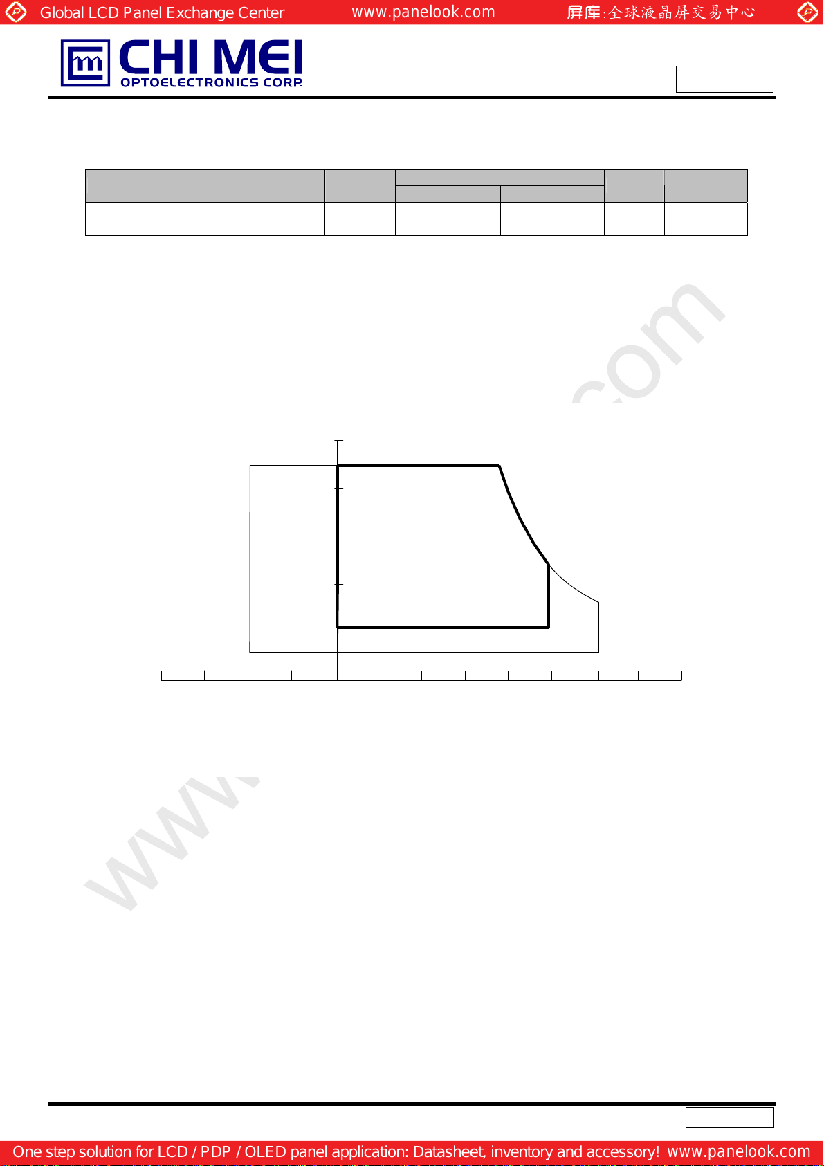
Note (1) Temperature and relative humidity range is shown in the figure below.
(a) 90 %RH Max. (Ta ≦ 40 ºC).
(b) Wet-bulb temperature should be 39 ºC Max. (Ta > 40 ºC).
(c) No condensation.
Note (2) The temperature of panel display surface area should be 0 ºC Min. and 60 ºC Max.
Min. Max.
Relative Humidity (%RH)
Value
Doc No.: 1406Y327
Issued Date: Sep. 17, 2007
Model No.: M190A1-PS1
Approval
Unit Note
100
90
80
60
Operating Range
40
20
10
Storage Range
8060 -20 400 20-40
Temperature (ºC)
5 / 28
Version 2.2
One step solution for LCD / PDP / OLED panel application: Datasheet, inventory and accessory!
www.panelook.com
Page 6
Global LCD Panel Exchange Center
www.panelook.com
2.2 ABSOLUTE RATINGS OF ENVIRONMENT (OPEN CELL)
High temperature or humidity may reduce the performance of panel. Please store LCD panel within the
specified storage conditions.
Storage Condition: With packing.
Storage temperature range: 25±5 ºC.
Storage humidity range: 50±10%RH.
Shelf life: 30days
2.3 ELECTRICAL ABSOLUTE RATINGS (OPEN CELL)
Item Symbol
Power Supply Voltage for
LCD
Logic Input Voltage V5A -0.3 6.0 V
Logic Input Voltage VDD -0.3 4.3 V
Note (1) Permanent damage might occur if the module is operated at conditions exceeding the maximum
Vin 13.2 14.4 V
Min. Max.
Value
Doc No.: 1406Y327
Issued Date: Sep. 17, 2007
Model No.: M190A1-PS1
Approval
Unit Note
(1)
values.
6 / 28
Version 2.2
One step solution for LCD / PDP / OLED panel application: Datasheet, inventory and accessory!
www.panelook.com
Page 7
Global LCD Panel Exchange Center
www.panelook.com
Doc No.: 1406Y327
Issued Date: Sep. 17, 2007
Model No.: M190A1-PS1
Approval
3. ELECTRICAL CHARACTERISTICS (OPEN CELL)
3.1 TFT LCD OPEN CELL Ta = 25 ± 2 ºC
Parameter SYMBOL
Power Supply Voltage for LCD Vin 13.2 13.8 14.4 V Power Supply Current for LCD Iin - 300 - mA Logic Input Voltage V5A 4.75 5 5.25 V Reserve
Logic Input Current I5A - 25 - mA Reserve
Driver Logic Input V oltage VDD - 3.3 - V Driver Logic Input Current IDD - 55 - mA Differential Impendence Zm - 100 -
LCD Inrush Current Irush - 3 - A -
High 2.5 3.3 - V - PANEL On
Low
High 2.5 3.3 V - DCDC On
Low
High VCOM_PWM 2.5 - V - VCOM PWM
Low - - 0.6 V -
VCOM PWM Frequency VCOM_PWM - 27 - KHz Adjustable Duty
Note (1) The module is recommended to operate within specification ranges listed above for normal
PANEL_ON
DCDC_ ON
MIN TYP MAX
- - 0.6 V -
- - 0.6 V -
Value
UNIT Note
Ω
-
Cycle
function.
7 / 28
Version 2.2
One step solution for LCD / PDP / OLED panel application: Datasheet, inventory and accessory!
www.panelook.com
Page 8
Global LCD Panel Exchange Center
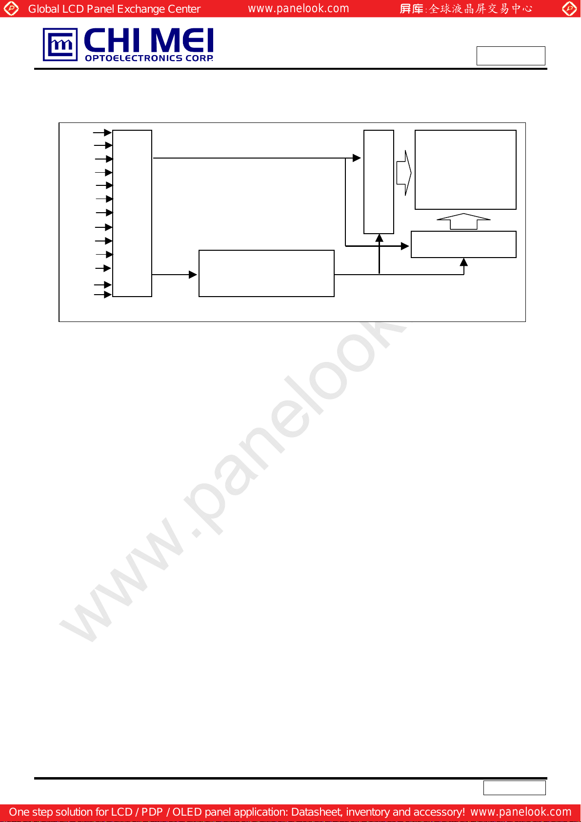
4. BLOCK DIAGRAM
4.1 TFT LCD MODULE
FR0~2(+/-)
FB0~2(+/-)
FG0~2(+/-)
FCK(+/-)
BR0~2(+/-)
BG0~2(+/-)
BB0~2(+/-)
BCK(+/-)
F/BSTHI
Panel On
DC/DC ON
Vin,V5A,VDD
GND
INPUT CONNECTOR
(IL-FHR-F36S-HF)
www.panelook.com
DC/DC CONVERTER &
REFERENCE VOLTAGE
Doc No.: 1406Y327
Issued Date: Sep. 17, 2007
Model No.: M190A1-PS1
SCAN DRIVER IC
TFT LCD PANEL
(1440x3x900)
DA TA DRIVER IC
Approval
8 / 28
Version 2.2
One step solution for LCD / PDP / OLED panel application: Datasheet, inventory and accessory!
www.panelook.com
Page 9
Global LCD Panel Exchange Center
5. INPUT TERMINAL PIN ASSIGNMENT
5.1 TFT LCD MODULE
(1)CN1 (Panel Interface)
Pin Name Description
1 Vin Driver Power Input Voltage
2 Vin Driver Power Input Voltage
3 V5A Logic Input Voltage +5V
4 PANEL_ON
5 DCDC_ON
6 VCM_PWM
7 GVOFF Gate driver high voltage switch timing control.
8 NC No connect
9 GND Ground
10 BSTHI Data driver start pulse input(Back)
11 GND Ground
12 BR0N Negative RSDS differential data input. Channel R0(Back)
13 BR0P Positive RSDS differential data input. Channel R0(Back)
14 BR1N Negative RSDS differential data input. Channel R1(Back)
15 BR1P Positive RSDS differential data input. Channel R1(Back)
16 BR2N Negative RSDS differential data input. Channel R2(Back)
17 BR2P Positive RSDS differential data input. Channel R2(Back)
18 GND Ground
19 BCKN Negative RSDS differential clock input. (Back)
20 BCKP Positive RSDS differential clock in put. (Back)
21 GND Ground
22 BG0N Negative RSDS differential data input. Channel G0(Back)
23 BG0P Positive RSDS differential data input. Channel G0(Back)
24 BG1N Negative RSDS differential data input. Channel G1(Back)
25 BG1P Positive RSDS differential data input. Channel G1(Back)
26 BG2N Negative RSDS differential data input. Channel G2(Back)
27 BG2P Positive RSDS differential data input. Channel G2(Back)
28 GND Ground
29 BB0N Negative RSDS differential data input. Channel B0(Back)
30 BB0P Positive RSDS differential data input. Channel B0(Back)
31 BB1N Negative RSDS differential data input. Channel B1(Back)
32 BB1P Positive RSDS differential data input. Channel B1(Back)
33 BB2N Negative RSDS differential data input. Channel B2(Back)
34 BB2P Positive RSDS differential data input. Channel B2(Back)
35 GND Ground
36 GND Ground
This pin is used to control the driver Logic Input Voltage VDD. When
PANEL_ON input is “H”, VDD will be to driver.
This pin is used to control the PWM IC. When DCDC_ON input is “H”, it enable
PWM IC.
This pin is used to generate common voltage for panel. Adjust pulse width could
be changed common voltage.
www.panelook.com
Doc No.: 1406Y327
Issued Date: Sep. 17, 2007
Model No.: M190A1-PS1
Approval
9 / 28
Version 2.2
One step solution for LCD / PDP / OLED panel application: Datasheet, inventory and accessory!
www.panelook.com
Page 10

Global LCD Panel Exchange Center
(2)CN2 (Panel Interface)
Pin Name Description
1 VDD Driver Logic Input Voltage
2 VDD Driver Logic Input Voltage
3 XAO
4 STV
5 CKV Gate driver shift clock
6 OE
7 GND Ground
8 FR0N Negative RSDS differential data input. Channel R0(Front)
9 FR0P Positive RSDS differential data input. Channel R0(Front)
10 FR1N Negative RSDS differential data input. Channel R1(Front)
11 FR1P Positive RSDS differential data input. Channel R1(Front)
12 FR2N Negative RSDS differential data input. Channel R2(Front)
13 FR2P Positive RSDS differential data input. Channel R2(Front)
14 GND Ground
15 POL Data driver polarity inverting input
16 STB
17 GND Ground
18 FCKN Negative RSDS differential clock input. (Front)
19 FCKP Positive RSDS differential clock input. (Front)
20 GND Ground
21 FG0N Negative RSDS differential data input. Channel G0(Front)
22 FG0P Positive RSDS differential data input. Channel G0(Front)
23 FG1N Negative RSDS differential data input. Channel G1(Front)
24 FG1P Positive RSDS differential data input. Channel G1(Front)
25 FG2N Negative RSDS differential data input. Channel G2(Front)
26 FG2P Positive RSDS differential data input. Channel G2(Front)
27 GND Ground
28 FB0N Negative RSDS differential data input. Channel B0(Front)
29 FB0P Positive RSDS differential data input. Channel B0(F ront)
30 FB1N Negative RSDS differential data input. Channel B1(Front)
31 FB1P Positive RSDS differential data input. Channel B1(F ront)
32 FB2N Negative RSDS differential data input. Channel B2(Front)
33 FB2P Positive RSDS differential data input. Channel B2(F ront)
34 FSTHI Data driver start pulse input (Front)
35 GND Ground
36 GND Ground
Note (1) Connector Part No.: IL-FHR-F36S-HF.
When /XAO input pin is low, all the Gate driver output pins are forced to VGH
level. Note that this pin has higher priority than OE.
Gate driver start pulse is read at the rising edge of CKV and a scan signal is
output from the gate driver output pin.
This pin is used to control the Gate driver output. When OE input is “H”, gate
driver output is fixed to VGL level regardless CKV.
The contents of the data driver register are transferred to the latch circuit at the
rising edge of STB. Then the gray scale voltage is output from the device at the
falling edge of STB.
www.panelook.com
Doc No.: 1406Y327
Issued Date: Sep. 17, 2007
Model No.: M190A1-PS1
Approval
10 / 28
Version 2.2
One step solution for LCD / PDP / OLED panel application: Datasheet, inventory and accessory!
www.panelook.com
Page 11

Global LCD Panel Exchange Center
5.2 COLOR DATA INPUT ASSIGNMENT
The brightness of each primary color (red, green and blue) is based on the 6-bit gray scale data input for
the color. The higher the binary input, the brighter the color. The table below provides the assignment of
color versus data input.
Color
R5 R4 R3 R2 R1 R0 G5 G4 G3 G2 G1 G0 B5 B4 B3 B2 B1 B0
Basic
Colors
Gray
Scale
Of
Red
Black
Red
Green
Blue
Cyan
Magenta
Yellow
White
Red(0) / Dark
Red(1)
Red(2)
:
:
Red(61)
Red(62)
Red(63)
0
0
1
1
0
0
0
0
0
0
1
1
1
1
1
1
0
0
0
0
0
0
:
:
:
:
1
1
1
1
1
1
www.panelook.com
Data Signal
Red Green Blue
0
0
0
0
0
0
0
0
0
0
0
0
0
1
1
1
1
0
0
0
0
0
0
0
0
0
0
0
0
0
1
1
1
1
1
1
0
0
0
0
0
0
0
0
0
0
0
0
0
1
1
1
0
0
0
0
1
1
1
1
1
1
1
1
1
1
1
1
1
0
0
0
0
0
0
1
1
1
1
1
1
1
1
1
1
1
1
1
0
0
0
1
1
1
1
1
1
1
1
1
1
1
1
1
0
0
0
0
0
0
0
0
0
0
0
0
0
0
0
0
1
0
0
0
0
0
0
0
0
0
0
0
1
0
0
0
0
0
0
0
0
0
0
:
:
:
:
:
:
:
:
:
:
:
:
:
:
:
:
:
:
:
:
:
:
:
:
:
:
1
1
0
1
0
0
0
0
0
0
0
0
0
1
1
1
0
0
0
0
0
0
0
0
0
0
1
1
1
1
0
0
0
0
0
0
0
0
0
Doc No.: 1406Y327
Issued Date: Sep. 17, 2007
Model No.: M190A1-PS1
Approval
0
0
0
0
0
0
0
0
0
1
1
1
1
1
1
1
1
1
0
0
0
1
1
1
0
0
0
0
0
0
0
0
0
:
:
:
:
:
:
0
0
0
0
0
0
0
0
0
Green(0) / Dark
Gray
Scale
Of
Green
Gray
Scale
Of
Blue
Note (1) 0: Low Level Voltage, 1: High Level Voltage
Green(1)
Green(2)
:
:
Green(61)
Green(62)
Green(63)
Blue(0) / Dark
Blue(1)
Blue(2)
:
:
Blue(61)
Blue(62)
Blue(63)
0
0
0
0
0
0
0
0
0
0
0
0
0
0
0
0
0
0
0
0
0
:
:
:
:
:
:
:
:
:
:
:
:
:
:
0
0
0
0
0
0
1
0
0
0
0
0
0
1
0
0
0
0
0
0
1
0
0
0
0
0
0
0
0
0
0
0
0
0
0
0
0
0
0
0
0
0
:
:
:
:
:
:
:
:
:
:
:
:
:
:
0
0
0
0
0
0
0
0
0
0
0
0
0
0
0
0
0
0
0
0
0
0
0
0
0
0
0
0
0
0
0
0
0
0
0
0
1
0
0
0
0
0
0
0
0
0
1
0
0
0
0
0
0
0
:
:
:
:
:
:
:
:
:
:
:
:
:
:
:
:
:
:
:
:
:
:
1
1
1
0
1
0
0
0
0
0
0
1
1
1
1
0
0
0
0
0
0
0
1
1
1
1
1
0
0
0
0
0
0
0
0
0
0
0
0
0
0
0
0
0
0
0
0
0
0
0
0
0
0
0
1
0
0
0
0
0
0
0
0
0
1
0
:
:
:
:
:
:
:
:
:
:
:
:
:
:
:
:
:
:
:
:
:
:
0
0
0
0
0
1
1
1
1
0
1
0
0
0
0
0
1
1
1
1
1
0
0
0
0
0
0
1
1
1
1
1
1
11 / 28
Version 2.2
One step solution for LCD / PDP / OLED panel application: Datasheet, inventory and accessory!
www.panelook.com
Page 12

Global LCD Panel Exchange Center
6. INTERFACE TIMING
6.1 INPUT SIGNAL TIMING SPECIFICATIONS
FCKP-FCKN/
BCKP-BCKN
FSTHI/BSTHI
BR0P-BR0N
FR0P-FR0N
BR1P-BR1N
FR1P-FR1N
www.panelook.com
D00
D01
D00
D02
D03
D02
D01 D00
D03 D02
Doc No.: 1406Y327
Issued Date: Sep. 17, 2007
Model No.: M190A1-PS1
Approval
D01 D00 D01
D03 D02 D03
BR2P-BR2N
FR2P-FR2N
BG0P-BG0N
FG0P-FG0N
BG1P-BG1N
FG1P-FG1N
BG2P-BG2N
FG2P-FG2N
BB0P-BB0N
FB0P-FB0N
BB0P-BB0N
FB0P-FB0N
BB0P-BB0N
FB0P-FB0N
D04
D10
D12
D14
D20
D22
D24
D05
D11
D13
D15
D21
D23
D25
D04
D10
D12
D14
D20
D22
D24
D05 D04
D11 D10
D13 D12
D15 D14
D21 D20
D23 D22
D25 D24
D05 D04 D05
D11 D10 D11
D13 D12 D13
D15 D14 D15
D21 D20 D21
D23 D22 D23
D25 D24 D25
1st Data
2nd Data
3rd Data
12 / 28
Version 2.2
One step solution for LCD / PDP / OLED panel application: Datasheet, inventory and accessory!
www.panelook.com
Page 13

Global LCD Panel Exchange Center
www.panelook.com
Doc No.: 1406Y327
Issued Date: Sep. 17, 2007
Model No.: M190A1-PS1
Approval
6.2 POWER ON/OFF SEQUENCE
To prevent a latch-up or DC operation of LCD module, the power on/off sequence should be as the diagram
below.
Parameter Symbol Condition
Panel On to DC/DC On t1 - 10 - DC/DC On to RSDS Data t2 - - 50 RSDS Data to BL_On t3 - - 200 RSDS Data Off to Panel Off t4 - - 100 -
Panel On
Min. Typ. Max.
Spec
Unit
mS
DC/DC On
Tcon
BL_ON
t1
t2
t3
t4
13 / 28
Version 2.2
One step solution for LCD / PDP / OLED panel application: Datasheet, inventory and accessory!
www.panelook.com
Page 14

Global LCD Panel Exchange Center
7. Driver DC CHARACTERISTICS
7.1 RSDS CHARACTERISTICS
( VDD = 2.3 to 3.6 V, VDDA = 8.0 to 13.5 V, VSSD = VSSA = 0V)
Parameter Symbol Condition Min. Typ. Max. Unit
RSDS high input voltage V
RSDS low input voltage V
RSDS common mode
input voltage range
RSDS input leakage
current
Note: (1) VCMRSDS = (VCLKP + VCLKN) / 2 or VCMRSDS = (VDxxP + VDxxN) / 2
(2) VDIFFRSDS = VCLKP - VCLKN or VDIFFRSDS = VDxxP – VDxxN
DIFFRSDS
DIFFRSDS
V
CMRSDS
IDL
www.panelook.com
V
V
V
DxxP, DxxN, CLKP,
CLKN
CMRSDS
CMRSDS
DIFFRSDS
= + 1.2 V
= + 1.2 V
= + 200 mV
Doc No.: 1406Y327
Issued Date: Sep. 17, 2007
Model No.: M190A1-PS1
Approval
(1)
100 200 -
(1)
- -200 - 100
VSSD +
(2)
0.1
-10 - 10 µA
- VDDD - 1.2 V
mV
CLKN
CLKP
CLKP-CLKN
V
DIFFRSDS
V
DIFFRSDS
V
DIFFRSDS
V
DIFFRSDS
V
CMRSDS
GND
0V
14 / 28
Version 2.2
One step solution for LCD / PDP / OLED panel application: Datasheet, inventory and accessory!
www.panelook.com
Page 15

Global LCD Panel Exchange Center
www.panelook.com
Doc No.: 1406Y327
Issued Date: Sep. 17, 2007
Model No.: M190A1-PS1
7.2 ELECTRICAL CHARACTERISTICS (VSSD=VSSA=0V)
Parameter Symbol Condition
RSDS input “Low”
Voltage
RSDS input “High”
Voltage
RSDS reference
voltage
V
DIFFRSDS
V
DIFFRSDS
V
CMRSDS
Input “Low” voltage VIL 0 - 0.2VDDD µA
Input “High” voltage VIH 0.8VDDD - VDDD µA
Input leak current IL
Supply current
(In operation mode)
Supply current
(In stand-by mode)
Pull high resistance Rpu
- -200 - mV
DX[2:0]P,DX[2:0]N,
- 200 - mV
CLKP,CLKN
EIO1,EIO2,DIR,TP1,
POL
VDDD=3.6V - - Note(1) mA
I
CCD1
VDDD=3.6V - - Note(2) mA
I
CCD2
/POLINV,RS,
ENREOP,VC
Min. Typ. Max.
VSSD+0.1 1.2 VDDD-1.2 V
-1 - 1 µA
0.9Typ 800 1.1Typ
Pull low resistance Rpd POL20,/LP 0.9Typ 190 1.1Typ
Note: (1) Test condition: TP1= 20µs, CLK =54MHz, data pattern =1010….checkerboard pattern, Ta=25℃
Spec
Approval
Unit
kΩ
kΩ
(2) No load condition
15 / 28
Version 2.2
One step solution for LCD / PDP / OLED panel application: Datasheet, inventory and accessory!
www.panelook.com
Page 16

Global LCD Panel Exchange Center
S
80%
)
)
80%
8. Driver AC CHARACTERISTICS
Parameter Symbol Condition
Clock pulse width t
Clock pulse low period t
Clock pulse high period t
Data setup time t
Data hold time t
Start pulse setup time t
Start pulse hold time t
Last data CLK to TP1 high
TP1 high to EIOn high t
POL to TP1 setup time t
TP1 to POL hold time t
CLK
CLK(L)
CLK(H)
SETUP1
HOLD1
SETUP2
HOLD2
t
TP1(H)
t
LAST
NEXT
POL-TP1
TP1-POL
www.panelook.com
Doc No.: 1406Y327
Issued Date: Sep. 17, 2007
Model No.: M190A1-PS1
Approval
Spec
Min. Typ. Max.
- 11 - - ns
- 5 - - ns
- 5 - - ns
- 2 - - ns
- 0 - - ns
- 1 - - ns
- 2 - - ns
- 15 - - CLKPTP1 high period
- 0 - - CLKP
- 6 - - CLKP
POL toggle to TP1 rising 3 - - ns
TP1 falling to POL toggle 2 - - ns
Unit
CLKP-CLKN
D**P – D**N
(RSDS)
BSTHI
F
D**P – D**N
CLKP-CLKN
(RSDS)
THI
(RSDS)
STB
POL
t
CLK
t
SETUP2
t
CLK(L
t
HOLD2
LAST-2
Even Odd Even
t
CLK(H
LAST-1
Odd
Even
LAST
Odd
t
POL-TP1
t
SETUP1
t
LAST
t
HOLD1
t
SETUP1
Invalid Data
t
t
HOLD1
t
TP1- POL
20%
20%
80%
80%
20%
80%
20%
80%
16 / 28
Version 2.2
One step solution for LCD / PDP / OLED panel application: Datasheet, inventory and accessory!
www.panelook.com
Page 17

Global LCD Panel Exchange Center
www.panelook.com
Doc No.: 1406Y327
Issued Date: Sep. 17, 2007
Model No.: M190A1-PS1
Approval
9. VERTICAL TIMING
Parameter Symbol Condition
CKV period t
CKV pulse width t
OE pulse width tOE - 1 - /XAO pulse width t
Data setup time tSU - 700 - - ns
Data hold time tHD - 700 - - ns
OE to CKV time t
STB to CKV t
STB Pulse Width t
GVOFF to CKV t
GVOFF Pulse width(Note1) t
Note 1:GVOFF, OE, STB frequency same as CKV
- 5 - -
CKV
, t
CKVH
WXAO
OE-CKV
STB-CKV
- - 0.5 - µs
STB
GVOFF-CKV
GVOFF
50% duty cycle 2.5 - -
CKVL
- 6 - -
- - 0.5 - µs
- 0 0 0 µs
- - -0.5 - µs
- - 9.0 - µs
Min. Typ. Max.
Spec
Unit
µs
CKV
STV
OE
STB
t
SU
OE-CKV
t
t
OE
t
HD
t
CKV
t
STB-CKV
t
CKVH CKVL
t
50%
50%
50%
t
CKV-GVOFF
GVOFF
t
GVOFF
17 / 28
Version 2.2
One step solution for LCD / PDP / OLED panel application: Datasheet, inventory and accessory!
www.panelook.com
Page 18

Global LCD Panel Exchange Center
10. OPTICAL CHARACTERISTICS
10.1 TEST CONDITIONS
Item Symbol Value Unit
Ambient Temperature Ta
Ambient Humidity Ha
Supply Voltage VCC 5.0 V
Input Signal According to typical value in "3. ELECTRICAL CHARACTERISTICS"
Lamp Current IL 7.0 mA
Inverter Operating Frequency FL 61 KHz
10.2 OPTICAL SPECIFICATIONS
The relative measurement methods of optical characteristics are shown as below. The following items
should be measured under the test conditions described in 9.1 and stable environment shown in Note (6).
Item Symbol Condition Min. Typ. Max. Unit Note
Red
Color
Chromaticity
Center Transmittance T%
Contrast Ratio CR
Response Time
Transmittance uniformity
Viewing Angle
Green
Blue
White
Horizontal
Vertical
www.panelook.com
Doc No.: 1406Y327
Issued Date: Sep. 17, 2007
Model No.: M190A1-PS1
Approval
o
25±2
50±10
Rcx 0.649
Rcy
0.332
Gcx 0.274
θ
=0°, θY =0°
Gcy
Bcx 0.148
Standard light source “C”
x
CS-1000T
Typ -
0.03
Bcy
0.589
0.101
Typ +
0.03
Wcx 0.320
Wcy
TR
T
F
δT%
θ
+
x
θ
-
x
θ
+
Y
θ
-
Y
θ
=0°, θY =0°
x
CS-1000T, CMO BLU
θ
=0°, θY =0°
x
θ
=0°, θY =0°
x
CA-210
CR≥10
CA-210
5.4 6.0 - %
500 700
0.356
-
-
-
1.5 6.5 ms
3.5 8.5 ms
- 1.25 1.4 -
75 85
75
85
70
80
70
80
-
-
-
-
C
%RH
-
-
-
-
-
-
-
-
- (1), (3)
Deg.
(0),(6)
(1), (8)
(4)
(1), (7)
(1), (2)
(6)
18 / 28
Version 2.2
One step solution for LCD / PDP / OLED panel application: Datasheet, inventory and accessory!
www.panelook.com
Page 19

Global LCD Panel Exchange Center
10.3 FLICKER ADJUSTMENT
(1)Adjustment Pattern:
Depend on User’s Timing Controller Selection
(2) Adjustment Method:
Flicker should be adjusted by turning the duty of VCM_PWM (refer to 5.1). It is adjusted to the point with
least flickering of the whole screen. After making it surely overrun at once, it should be adjusted to the
optimum point.
www.panelook.com
Doc No.: 1406Y327
Issued Date: Sep. 17, 2007
Model No.: M190A1-PS1
Approval
19 / 28
Version 2.2
One step solution for LCD / PDP / OLED panel application: Datasheet, inventory and accessory!
www.panelook.com
Page 20

Global LCD Panel Exchange Center
Note (0) Light source is the standard light source “C” which is defined by CIE and driving voltages are based
on suitable gamma voltages. The calculating method is as following:
Measure Module’s and BLU’s spectrums. White is without signal input and R, G, B are with signal input.
BLU(for A190A2 BLU) is supplied by CMO.
Calculate cell’s spectrum.
Calculate cell’s chromaticity by using the spectrum of standard light source “C”
Note (1) Light source is the BLU which is supplied by CMO and driving voltages are based on suitable
gamma voltages.
Note (2) Definition of Viewing Angle (θx, θy):
www.panelook.com
Doc No.: 1406Y327
Issued Date: Sep. 17, 2007
Model No.: M190A1-PS1
Approval
Note (3) Definition of Contrast Ratio (CR):
θX- = 90º
6 o’clock
θ
y- = 90º
x-
y-
Normal
θx = θy = 0º
θy- θy+
θx−
θx+
12 o’clock direction
y+
θ
y+ = 90º
x+
θX+ = 90º
The contrast ratio can be calculated by the following expression.
Contrast Ratio (CR) = L255 / L0
L255: Luminance of gray level 255
L 0: Luminance of gray level 0
CR = CR (1)
CR (X) is corresponding to the Contrast Ratio of the point X at Figure in Note (7).
20 / 28
Version 2.2
One step solution for LCD / PDP / OLED panel application: Datasheet, inventory and accessory!
www.panelook.com
Page 21

Global LCD Panel Exchange Center
T
.67 ms
Note (4) Definition of Response Time (TR, TF):
www.panelook.com
Doc No.: 1406Y327
Issued Date: Sep. 17, 2007
Model No.: M190A1-PS1
Approval
100%
90%
Optical
Response
Gray Level 255
10%
0%
Note (5) Definition of Luminance of White (L
Measure the luminance of gray level 255 at center point
L
= L (1)
C
L (x) is corresponding to the luminance of the point X at Figure in Note (7).
T
R
66.67 ms
Gray Level 255
ime
T
F
66
):
C
Note (6) Measurement Setup:
The LCD module should be stabilized at given temperature for 20 minutes to avoid abrupt
temperature change during measuring. In order to stabilize the luminance, the measurement
should be executed after lighting Backlight for 20 minutes in a windless room.
LCD Module
LCD Panel
Center of the Screen
500 mm
CA-210
CS-1000T
Field of View = 2º
Light Shield Room
(Ambient Luminance < 2 lux)
21 / 28
Version 2.2
One step solution for LCD / PDP / OLED panel application: Datasheet, inventory and accessory!
www.panelook.com
Page 22

Global LCD Panel Exchange Center
X
A
r
Note (7) Definition of Transmittance Variation (δT%):
Measure the transmittance at 13 points
www.panelook.com
Doc No.: 1406Y327
Issued Date: Sep. 17, 2007
Model No.: M190A1-PS1
Approval
Maximum [L (1), L (2),……….L (12), L (13)]
δT% =
Minimum [L (1), L (2),…… ….L (12), L (13)]
Horizontal Line Numbe
7
23
1
45
W/4 W/4 W/4 W/4
W
H/4
H
Vertical Line Number
H/4 H/4 H/4
10mm
6
9 10
11 12
10mm 10mm
10mm
8
:Test Point
X=1 to 13
13
Note (8) Definition of Transmittance (T%):
Module is without signal input.
Transmittance =
ctive area
Luminance of LCD module
* 100%
Luminance of backlight
22 / 28
Version 2.2
One step solution for LCD / PDP / OLED panel application: Datasheet, inventory and accessory!
www.panelook.com
Page 23

Global LCD Panel Exchange Center
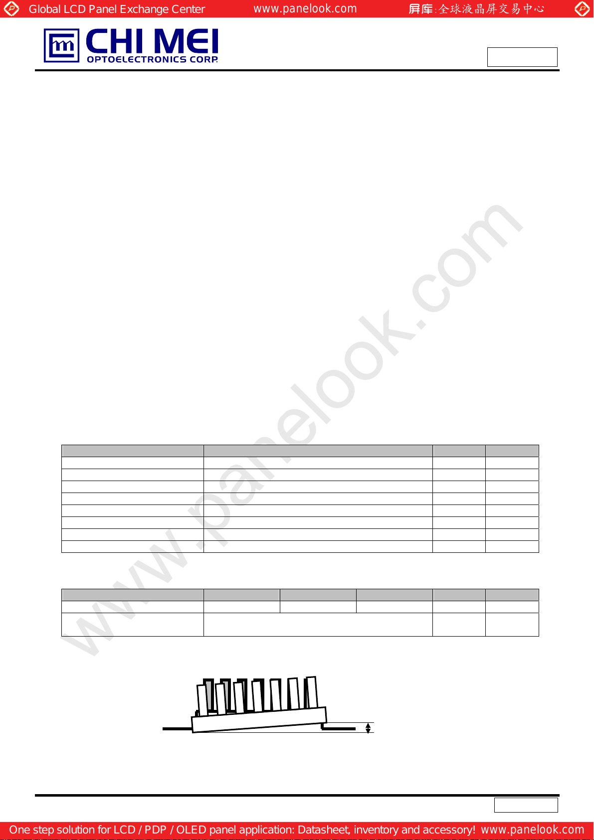
11. PACKAGING
11.1 PACKING SPECIFICATIONS
(1) 15 open cells / 1 Box
(2) Box dimensions: 615 (L) X 515 (W) X 385 (H) mm
(3) Weight: approximately 14.8Kg (15 open cells per box)
11.2 PACKING METHOD
(1) Carton Packing should have no failure in the following reliability test items.
Test Item Test Conditions Note
ISTA STANDARD
Packing
Vibration
Random, Frequency Range: 1 – 200 Hz
Top & Bottom: 30 minutes (+Z), 10 min (-Z),
Right & Left: 10 minutes (X)
Back & Forth 10 minutes (Y)
www.panelook.com
Doc No.: 1406Y327
Issued Date: Sep. 17, 2007
Model No.: M190A1-PS1
Approval
Non Operation
(2) Packing method.
23 / 28
Version 2.2
One step solution for LCD / PDP / OLED panel application: Datasheet, inventory and accessory!
www.panelook.com
Page 24

Global LCD Panel Exchange Center
www.panelook.com
Doc No.: 1406Y327
Issued Date: Sep. 17, 2007
Model No.: M190A1-PS1
Approval
24 / 28
Version 2.2
One step solution for LCD / PDP / OLED panel application: Datasheet, inventory and accessory!
www.panelook.com
Page 25

Global LCD Panel Exchange Center
12. DEFINITION OF LABELS
12.1 CMO OPEN CELL LABEL
The barcode nameplate is pasted on each OPEN CELL as illustration for CMO internal control.
Barcode definition:
www.panelook.com
Doc No.: 1406Y327
Issued Date: Sep. 17, 2007
Model No.: M190A1-PS1
Approval
Serial ID: CM
19A11 Model number M19A1-PS1=19A11
NNNN Serial number Manufacturing sequence of product
-19A11-X-X-X-XX-L-XX-L-YMD-NNNN
Code Meaning Description
CM Supplier code CMO=CM
X Revision code C1:1, C2:2,…
X Source driver IC code
X Gate driver IC code
XX Cell location Tainan, Taiwan=TN
L Cell line # 0~12=1~C
XX Module location Tainan, Taiwan=TN
L Module line # 0~12=1~C
Year, month, day Year: 2001=1, 2002=2, 2003=3, 2004=4…
YMD
Century=1, CLL=2, Demos=3, Epson=4, Fujitsu=5, Himax=6,
Hitachi=7, Hynix=8, LDI=9, Matsushita=A, NEC=B, Novatec=C,
OKI=D, Philips=E, Renasas=F, Samsung=G, Sanyo=H, Sharp=I,
TI=J, Topro=K, T oshiba =L, Windbond=M
Month: 1~12=1, 2, 3, ~, 9, A, B, C
Day: 1~31= 1, 2, 3, ~, 9, A, B, C, ~, T, U, V
25 / 28
Version 2.2
One step solution for LCD / PDP / OLED panel application: Datasheet, inventory and accessory!
www.panelook.com
Page 26

Global LCD Panel Exchange Center
12.2 CARTON LABEL
The barcode nameplate is pasted on each box as illustration, and its definitions are as following explanation
www.panelook.com
Doc No.: 1406Y327
Issued Date: Sep. 17, 2007
Model No.: M190A1-PS1
Approval
Model Name: M190A1 –PS1
Carton ID: CMO internal control
Quantities: 15 pcs
26 / 28
Version 2.2
One step solution for LCD / PDP / OLED panel application: Datasheet, inventory and accessory!
www.panelook.com
Page 27

Global LCD Panel Exchange Center
www.panelook.com
13. PRECAUTIONS
13.1 ASSEMBL Y AND HANDLING PRECAUTIONS
(1) Do not apply rough force such as bending or twisting to the product during assembly.
(2) To assemble backlight or install module into user’s system can be only in clean working areas. The
dust and oil may cause electrical short or worsen the polarizer.
(3) It’s not permitted to have pressure or impulse on the module be cause the LCD panel will be damaged.
(4) Always follow the correct power sequence when the product is connecting and operating. This can
prevent damage to the CMOS LSI chips during latch-up.
(5) Do not pull the I/F connector in or out while the module is operating.
(6) Use a soft dry cloth without chemicals for cleaning, because the surface of polarizer is very soft and
easily scratched.
(7) It is dangerous that moisture come into or contacted the product, because moisture may damage the
Doc No.: 1406Y327
Issued Date: Sep. 17, 2007
Model No.: M190A1-PS1
Approval
product when it is operating.
(8) High temperature or humidity may reduce the performance of module. Please store this product within
the specified storage conditions.
(9) When ambient temperature is lower than 10ºC may reduce the display quality. For example, the
response time will become slowly.
13.2 SAFETY PRECAUTIONS
(1) If the liquid crystal material leaks from the panel, it should be kept away from the eyes or mouth. In
case of contact with hands, skin or clothes, it has to be washe d away thoroughly with soap.
(2) After the product’s end of life, it is not harmful in case of normal operation and storage.
27 / 28
Version 2.2
One step solution for LCD / PDP / OLED panel application: Datasheet, inventory and accessory!
www.panelook.com
Page 28

Global LCD Panel Exchange Center
www.panelook.com
One step solution for LCD / PDP / OLED panel application: Datasheet, inventory and accessory!
www.panelook.com
 Loading...