

Page 1
PRODUCT SPECIFICATION
Doc. Number :
□ Tentative Specification
□ Preliminary Specification
■Approval Specification
MODEL NO.: M185BGE
SUFFIX: P03
Customer:
APPROVED BY SIGNATURE
Name / Title
Note
Product Version C1
Please return 1 copy for your confirmation with your
signature and comments.
Approved By Checked By Prepared By
吳柏勳
柯直孝
徐欣怡
Version 3.1 31 MAY 2012 24 / 23
The copyright belongs to CHIMEI InnoLux. Any unauthorized use is prohibited.
Page 2

PRODUCT SPECIFICATION
- CONTENTS -
1. GENERAL DESCRIPTION.......................................................................................................................4
1.1 OVERVIEW........................................................................................................................................4
1.2 GENERAL SPECIFICATI0NS...........................................................................................................4
2. MECHANICAL SPECIFICATIONS ..........................................................................................................4
3. ABSOLUTE MAXIMUM RATINGS ..........................................................................................................4
3.1 ABSOLUTE RATINGS OF ENVIRONMENT..................................................................................4
3.2 ELECTRICAL ABSOLUTE RATINGS.............................................................................................5
3.2.1 TFT LCD MODULE ..............................................................................................................5
3.3 ABSOLUTE RATINGS OF ENVIRONMENT (OPEN CELL).........................................................5
4. ELECTRICAL SPECIFICATIONS............................................................................................................6
4.1 FUNCTION BLOCK DIAGRAM......................................................................................................6
4.2. INTERFACE CONNECTIONS.........................................................................................................6
4.3 ELECTRICAL CHARACTERISTICS...............................................................................................8
4.4 Vcc POWER DIP CONDITION.......................................................................................................10
4.5 LVDS DATA MAPPING TABLE.....................................................................................................10
4.6 COLOR DATA INPUT ASSIGNMENT...........................................................................................10
4.7 DISPLAY TIMING SPECIFICATIONS...........................................................................................11
4.8 POWER ON/OFF SEQUENCE........................................................................................................13
5. OPTICAL CHARACTERISTICS.............................................................................................................14
5.1 TEST CONDITIONS........................................................................................................................14
5.2 OPTICAL SPECIFICATIONS..........................................................................................................14
5.3 Flicker Adjustment............................................................................................................................18
6. RELIABILITY TEST ITEM.......................................................................................................................19
7. LABEL........................................................................................................................................................20
7.1 CMI OPEN CELL LABEL...............................................................................................................20
8. PACKING...................................................................................................................................................21
8.1 Packing Information..........................................................................................................................21
8.2 CARTON...........................................................................................................................................21
8.3 PALLET ............................................................................................................................................22
9. PRECAUTIONS........................................................................................................................................23
9.1 HANDLING PRECAUTIONS.........................................................................................................23
9.2 SAFETY PRECAUTIONS...............................................................................................................23
9.3 OTHER..............................................................................................................................................23
10. OUTLINE DRAWING.............................................................................................................................23
Version 3.1 31 MAY 2012 24 / 23
The copyright belongs to CHIMEI InnoLux. Any unauthorized use is prohibited.
Page 3
PRODUCT SPECIFICATION
REVISION HISTORY
Version Date Page Description
3.0
3.1
FEB.21, 2012
May 31, 2012
All Spec Ver.1.0 was first issued.
Section 8 & 9 Hard Box packing
Version 3.1 31 MAY 2012 24 / 23
The copyright belongs to CHIMEI InnoLux. Any unauthorized use is prohibited.
Page 4
PRODUCT SPECIFICATION
1. GENERAL DESCRIPTION
1.1 OVERVIEW
The M185BGE-P03 is a 18.5” TFT LCD cell with driver ICs and a 30-pins-1ch-LVDS circuit board.
The product supports 1366 x 768 HDTV mode and can display up to 16.7M colors. The backlight unit
is not built in.
1.2 GENERAL SPECIFICATI0NS
Item Specification Unit Note
Screen Size 18.5” real diagonal
Driver Element a-si TFT active matrix - -
Pixel Number 1366 x R.G.B. x 768 pixel -
Pixel Pitch 0.3 (H) x 0.3 (V) mm -
Pixel Arrangement RGB vertical stripe - -
Display Colors 16.7M color -
Transmissive Mode Normally white - -
Surface Treatment Anti-Glare coating (Haze 25%), Hard coating (3H) - -
Power Consumption 6.3 Watt -
2. MECHANICAL SPECIFICATIONS
Item Min. Typ. Max. Unit Note
Weight
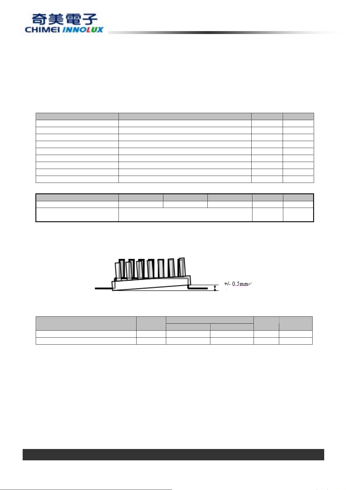
I/F connector mounting
position
Note (1) Please refer to the attached drawings for more information of front and back outline dimensions.
The mounting inclination of the connector makes
the screen center within ±0.5mm as the horizontal.
-
320.4 340.4 g -
- (2)
(2) Connector mounting position
(3) Please refer to sec.3.1 for more information of power consumption.
3. ABSOLUTE MAXIMUM RATINGS
3.1 ABSOLUTE RATINGS OF ENVIRONMENT
Item Symbol
Storage Temperature TST -20 +60 ºC (1)
Operating Ambient Temperature TOP 0 +50 ºC (1), (2)
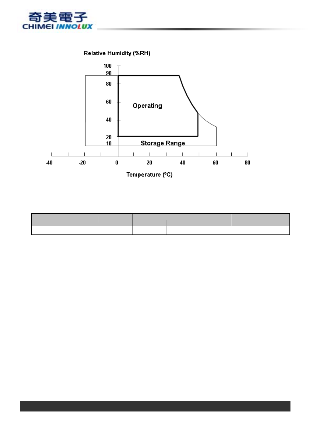
Note (1) (a) 90 %RH Max. (Ta <= 40 ºC).
(b) Wet-bulb temperature should be 39 ºC Max. (Ta > 40 ºC).
(c) No condensation.
Value
Min. Max.
Unit Note
Version 3.1 31 MAY 2012 24 / 23
The copyright belongs to CHIMEI InnoLux. Any unauthorized use is prohibited.
Page 5
PRODUCT SPECIFICATION
Note (2) The temperature of panel surface should be 0 ºC min. and 60 ºC max.
3.2 ELECTRICAL ABSOLUTE RATINGS
3.2.1 TFT LCD MODULE
Item Symbol
Power Supply Voltage VCC -0.3 6.0 V (1)
Note (1) Permanent damage to the device may occur if maximum values are exceeded. Function
operation should be restricted to the conditions described under Normal Operating Conditions.
Value
Min Max
Unit Note
3.3 ABSOLUTE RATINGS OF ENVIRONMENT (OPEN CELL)
High temperature or humidity may reduce the performance of panel. Please store LCD panel within the
specified storage conditions.
Storage Condition: With packing.
Storage temperature range: 25±5 ºC.
Storage humidity range: 50±10%RH.
Shelf life: 30days
Version 3.1 31 MAY 2012 24 / 23
The copyright belongs to CHIMEI InnoLux. Any unauthorized use is prohibited.
Page 6
PRODUCT SPECIFICATION
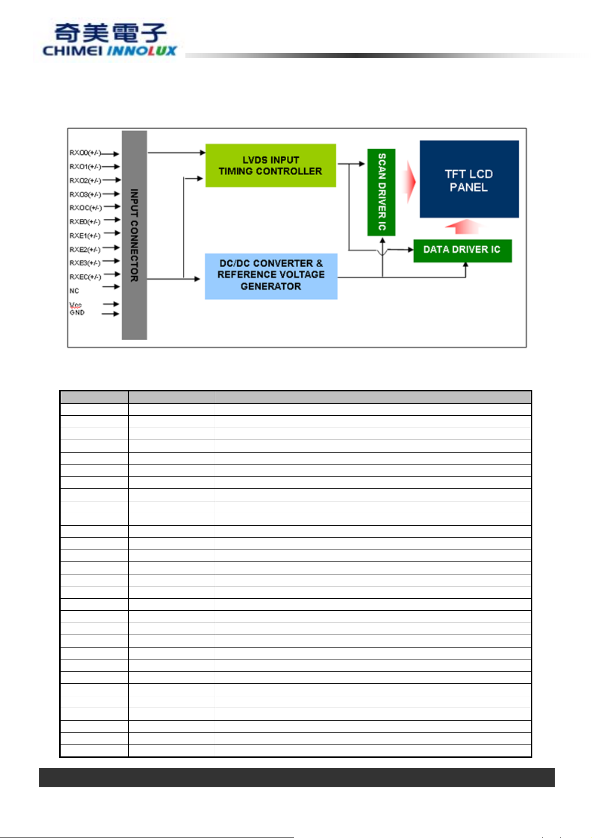
4. ELECTRICAL SPECIFICATIONS
4.1 FUNCTION BLOCK DIAGRAM
4.2. INTERFACE CONNECTIONS
PIN ASSIGNMENT
Pin Name Description
1 NC Not connection, this pin should be open.
2 NC Not connection, this pin should be open.
3 NC Not connection, this pin should be open.
4 GND Ground
5 RX0- Negative LVDS differential data input. Channel 0
6 RX0+ Positive LVDS differential data input. Channel 0
7 GND Ground
8 RX1- Negative LVDS differential data input. Channel 1
9 RX1+ Positive LVDS differential data input. Channel 1
10 GND Ground
11 RX2- Negative LVDS differential data input. Channel 2
12 RX2+ Positive LVDS differential data input. Channel 2
13 GND Ground
14 RXCLK- Negative LVDS differential clock input.
15 RXCLK+ Positive LVDS differential clock input.
16 GND Ground
17 RX3- Negative LVDS differential data input. Channel 3
18 RX3+ Positive LVDS differential data input. Channel 3
19 GND Ground
20 NC Not connection, this pin should be open.
21 NC Not connection, this pin should be open.
22 NC Not connection, this pin should be open.
23 GND Ground
24 GND Ground
25 GND Ground
26 Vcc +5.0V power supply
27 Vcc +5.0V power supply
28 Vcc +5.0V power supply
29 Vcc +5.0V power supply
Version 3.1 31 MAY 2012 24 / 23
The copyright belongs to CHIMEI InnoLux. Any unauthorized use is prohibited.
Page 7

PRODUCT SPECIFICATION
30 Vcc +5.0V power supply
Note (1) Connector Part No.:
GS23302-0011R-7H(FOXCONN) or 187106-30091[P-TWO(禾昌)]or equivalent
Note (2) The pixel is odd.
1,1
(odd)
2,1
3,1
1,2
(even)
2,2
1,3
(odd)
1,4
(even)
1,Xmax
Pitch
Pitch
Ymax,1
Ymax,
Xmax
Version 3.1 31 MAY 2012 24 / 23
The copyright belongs to CHIMEI InnoLux. Any unauthorized use is prohibited.
Page 8
PRODUCT SPECIFICATION
4.3 ELECTRICAL CHARACTERISTICS
Parameter Symbol
Power Supply Voltage Vcc
Ripple Voltage VRP
Rush Current I
White
Power Supply Current
Power Consumption PLCD - 2.75 3.85 Watt (4)
LVDS differential input voltage Vid
LVDS common input voltage Vic
Logic High Input Voltage VIH
Logic Low Input Voltage VIL
Note (1) The ambient temperature is Ta = 25 ± 2 ºC.
Black
Vertical Stripe
RUSH
Min. Typ. Max.
4.5 5 5.5
- -
- 1.5 2.0
- 350 450
- 550 700
- 550 700
100 - 600
1.0 1.2 1.4
- - 0.1
-0.1 - -
Value
0.3
Unit Note
V
V
A (2)
mA (3)a
mA (3)b
mA (3)c
mV
V
V
V
-
-
Note (2) Measurement Conditions:
Version 3.1 31 MAY 2012 24 / 23
The copyright belongs to CHIMEI InnoLux. Any unauthorized use is prohibited.
Page 9
PRODUCT SPECIFICATION
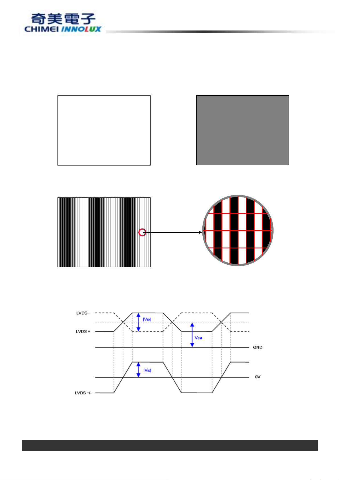
Note (3) The specified power supply current is under the conditions at Vcc = 5.0 V, Ta = 25 ± 2 ºC,
Fv = 75 Hz, whereas a power dissipation check pattern below is displayed.
a. White Pattern
c. Vertical Stripe Pattern
Active Area
b. Black Pattern
B
G
R
B
G
B
R
B
G
B
R
B
G
R R
R
R
R
G
G
G
G
B
B
B
B
R
R
Note (4) The power consumption is specified at the pattern with the maximum current.
Note (5) VID waveform condition
Active Area
Version 3.1 31 MAY 2012 24 / 23
The copyright belongs to CHIMEI InnoLux. Any unauthorized use is prohibited.
Page 10

PRODUCT SPECIFICATION
4.4 Vcc POWER DIP CONDITION
4.5 LVDS DATA MAPPING TABLE
LVDS Channel O0
LVDS Channel O1
LVDS Channel O2
LVDS Channel O3
LVDS output D7 D6 D4 D3 D2 D1 D0
Data order OG0 OR5 OR4 OR3 OR2 OR1 OR0
LVDS output D18 D15 D14 D13 D12 D9 D8
Data order OB1 OB0 OG5 OG4 OG3 OG2 OG1
LVDS output D26 D25 D24 D22 D21 D20 D19
Data order DE NA NA OB5 OB4 OB3 OB2
LVDS output D23 D17 D16 D11 D10 D5 D27
Data order NA OB7 OB6 OG7 OG6 OR7 OR6
4.6 COLOR DATA INPUT ASSIGNMENT
The brightness of each primary color (red, green and blue) is based on the 8-bit gray scale data input for
the color. The higher the binary input, the brighter the color. The table below provides the assignment of
color versus data input.
Data Signal
Basic
Colors
Gray
Scale
Of
Red
Gray
Scale
Of
Green
Color
Black
Red
Green
Blue
Cyan
Magenta
Yellow
White
Red(0) / Dark
Red(1)
Red(2)
:
:
Red(253)
Red(254)
Red(255)
Green(0) / Dark
Green(1)
Green(2)
:
:
Green(253)
R7 R6 R5 R4 R3 R2 R1 R0 R7 R6 G5 G4 G3 G2 G1 G0 R7 R6 B5 B4 B3 B2 B1 B0
0
0
1
1
0
0
0
0
0
0
1
1
1
1
1
1
0
0
0
0
0
0
:
:
:
:
1
1
1
1
1
1
0
0
0
0
0
0
:
:
:
:
0
0
Red Green Blue
0
0
0
0
0
0
0
0
0
0
0
0
1
1
1
1
1
1
0
0
0
0
0
0
0
0
0
0
0
0
1
1
1
1
1
1
0
0
0
0
0
0
0
0
0
0
0
0
0
0
0
0
0
0
1
1
1
1
1
1
1
1
1
1
1
1
0
0
0
0
0
0
1
1
1
1
1
1
1
1
1
1
1
1
1
1
1
1
1
1
1
1
1
1
1
1
0
0
0
0
0
0
0
0
0
0
0
0
0
0
0
0
0
1
0
0
0
0
0
0
0
0
0
0
1
0
0
0
0
0
0
0
:
:
:
:
:
:
:
:
:
:
:
:
:
:
:
:
:
:
:
:
:
:
:
:
1
1
1
1
0
1
0
0
0
0
0
0
1
1
1
1
1
0
0
0
0
0
0
0
1
1
1
1
1
1
0
0
0
0
0
0
0
0
0
0
0
0
0
0
0
0
0
0
0
0
0
0
0
0
0
0
0
0
0
0
0
0
0
0
0
0
0
0
0
0
0
0
:
:
:
:
:
:
:
:
:
:
:
:
:
:
:
:
:
:
:
:
:
:
:
:
0
0
0
0
0
0
1
1
1
1
1
1
0
0
0
0
0
0
0
0
0
0
0
0
1
1
0
0
0
0
0
0
1
1
1
1
1
1
1
1
1
1
0
0
1
1
1
1
1
1
0
0
0
0
1
1
1
1
1
1
0
0
0
0
0
0
0
0
0
0
0
0
0
0
0
0
0
0
:
:
:
:
:
:
:
:
:
:
:
:
0
0
0
0
0
0
0
0
0
0
0
0
0
0
0
0
0
0
0
0
0
0
0
0
0
1
0
0
0
0
1
0
0
0
0
0
:
:
:
:
:
:
:
:
:
:
:
:
0
1
0
0
0
0
0
0
0
0
0
0
0
0
0
0
0
0
1
1
1
1
1
1
1
1
1
1
1
1
0
0
0
0
1
1
1
1
0
0
0
0
0
0
0
0
0
0
0
0
:
:
:
:
:
:
:
:
0
0
0
0
0
0
0
0
0
0
0
0
0
0
0
0
0
0
0
0
0
0
0
0
:
:
:
:
:
:
:
:
0
0
0
0
Version 3.1 31 MAY 2012 24 / 23
The copyright belongs to CHIMEI InnoLux. Any unauthorized use is prohibited.
Page 11

PRODUCT SPECIFICATION
Green(254)
Green(255) 000 0 0 0 0 0 00000000111111111111110 1 0 0 0 0 0 0 0 0 00000000
Gray
Scale
Of
Blue
Blue(0) / Dark
Blue(1)
Blue(2)
:
:
Blue(253)
Blue(254)
Blue(255)
0
0
0
0
0
0
0
0
0
0
0
0
0
0
0
0
0
0
0
0
0
0
0
0
0
0
0
0
0
0
0
0
0
0
0
0
0
0
0
0
0
0
0
0
0
0
0
0
0
0
0
0
0
0
0
0
0
0
0
0
:
:
:
:
:
:
:
:
:
:
:
:
:
:
:
:
:
:
:
:
:
:
:
:
:
:
:
:
:
:
:
:
:
:
:
:
:
:
:
:
0
0
0
0
0
0
0
0
0
0
0
0
0
0
0
0
1
1
1
1
0
0
0
0
0
0
0
0
0
0
0
0
0
0
0
0
1
1
1
1
0
0
0
0
0
0
0
0
0
0
0
0
0
0
0
0
1
1
1
1
Note (1) 0: Low Level Voltage, 1: High Level Voltage
4.7 DISPLAY TIMING SPECIFICATIONS
The input signal timing specifications are shown as the following table and timing diagram.
Signal Item Symbol Min. Typ. Max. Unit Note
Frequency Fc 62.9 75.4 95.6 MHz -
Period Tc 10.5- 13.2 15.9- ns -
LVDS Clock
Vertical Display Term
Horizontal Display Term
Input cycle to
cycle jitter
Input Clock
to data skew
Spread
spectrum
modulation
range
Spread
spectrum
modulation
frequency
Frame Rate Fr 50 60 76 Hz Tv=Tvd+Tvb
Tot a l T v 800 806 815 Th -
Active
Display
Blank Tvb
Tot a l T h 1500 1560 1570 Tc Th=Thd+Thb
Active
Display
Blank Thb
T
-0.02*Tc -- 0.02*Tc ns (1)
rcl
TLVCCS -0.02*Tc - -0.02*T ps (2)
Fclkin_
mod
F
SSM
Tvd
Fc*97% - Fc*103% MHz
-- -- 100 KHz
-- 768 -- Th -
32 38 47 Th -
Thd
-- 1366 -- Tc --
134 194 204 Tc --
0
0
0
1
1
1
:
:
(3)
0
0
0
0
0
1
0
1
0
:
:
:
:
:
:
1
0
1
1
1
0
1
1
1
Version 3.1 31 MAY 2012 24 / 23
The copyright belongs to CHIMEI InnoLux. Any unauthorized use is prohibited.
Page 12

PRODUCT SPECIFICATION
Note:(0) Because this module is operated by DE only mode, Hsync and Vsync input signals are ignored.
Note (1) The input clock cycle-to-cycle jitter is defined as below figures. Trcl = I T1 – TI
T1
Note (2) The SSCG (Spread spectrum clock generator) is defined as below figures.
Version 3.1 31 MAY 2012 24 / 23
The copyright belongs to CHIMEI InnoLux. Any unauthorized use is prohibited.
Page 13

PRODUCT SPECIFICATION
Note (3) Input Clock to data skew is defined as below figures
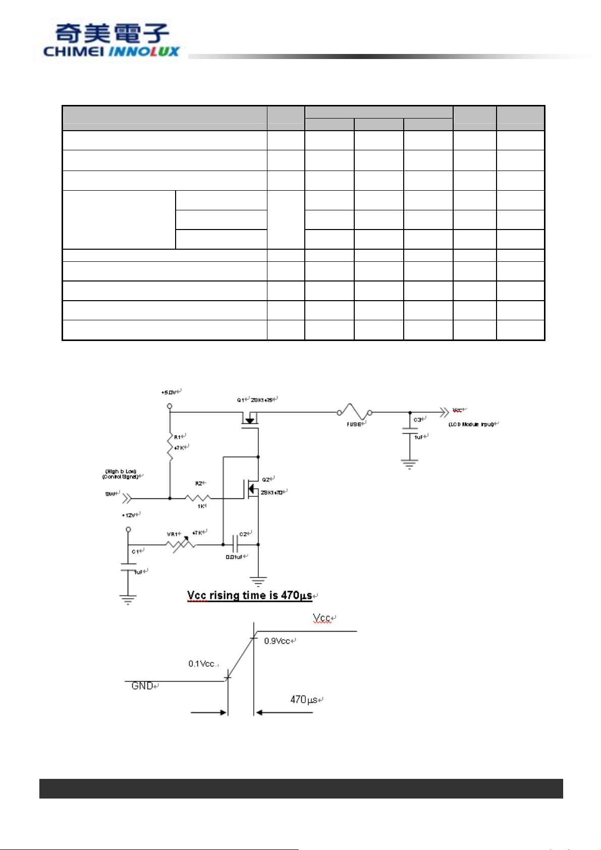
4.8 POWER ON/OFF SEQUENCE
To prevent a latch-up or DC operation of LCD module, the power on/off sequence should be as the
diagram below.
Timing Specifications:
Parameters
T1 0.1 - 10 ms
T2 0 30 50 ms
T3 200 250 - ms
T4 100 250- - ms
T5 0 20- 50 ms
T6 0.1 - 50 ms
T7 1000 - - ms
Min Typ. Max
Values
Units
Note (1) The supply voltage of the external system for the module input should be the same as the
definition of Vcc.
Note (2) When the backlight turns on before the LCD operation of the LCD turns off, the display may
momentarily become abnormal screen.
Version 3.1 31 MAY 2012 24 / 23
The copyright belongs to CHIMEI InnoLux. Any unauthorized use is prohibited.
Page 14

PRODUCT SPECIFICATION
Note (3) In case of VCC = off level, please keep the level of input signals on the low or keep a high
impedance.
Note (4) T4 should be measured after the module has been fully discharged between power off and on
period.
Note (5) Interface signal shall not be kept at high impedance when the power is on.
Note (6) CMI won’t take any responsibility for the products which are damaged by the customers not
following the Power Sequence.
Note (7) There might be slight electronic noise when LCD is turned off (even backlight unit is also off). To
avoid this symptom, we suggest "Vcc falling timing" to follow "t6 spec".
5. OPTICAL CHARACTERISTICS
5.1 TEST CONDITIONS
Item Symbol Value Unit
Ambient Temperature Ta
Ambient Humidity Ha
Supply Voltage VCC 5 V
Input Signal According to typical value in "4.3 ELECTRICAL CHARACTERISTICS"
LED Light Bar Input Current
Per Input Pin
PWM Duty Ratio D 100 %
LED Light Bar Test Converter TEST01001 T2-A1
5.2 OPTICAL SPECIFICATIONS
25±2
50±10
65 ± 1.9 mADC
I
PIN
o
C
%RH
The relative measurement methods of optical characteristics are shown as below. The following items
should be measured under the test conditions described in 5.1 and stable environment shown in Note (6).
Item Symbol Condition Min. Typ. Max. Unit Note
Rx 0.641
Ry 0.340
Gx 0.315
Gy 0.629
Bx 0.159
By 0.051
Wx 0.313
θx=0°, θY =0°
CS-2000
R=G=B=255
Gray Scale
Wy
Typ –
0.03
0.329
Typ +
0.03
-- (1), (5)
Color
Chromaticity
(CIE 1931)
Red
Green
Blue
White
Center Transmittance T% -- 6.2 -- % (1), (5)
Contrast Ratio CR
Response Time
White Variation
Viewing Angle
Viewing Angle
TR - 1.5 4.0
TF
δW
Horizontal x - + x+ 80 90 -
Vertica l y - + y+
Horizontal x - + x+ 100 110 ---
Vertica l y - + y+
θx=0°, θY =0°
θx=0°, θY =0°
USB2000
CR 10≧
USB2000
CR 5≧
USB2000
500 700 - - (2), (5)
- 3.5 6.0
ms (3)
75 - - % (5), (6)
55 65 -
75 85
Deg. (1), (6)
Deg. (1), (5)
Version 3.1 31 MAY 2012 24 / 23
The copyright belongs to CHIMEI InnoLux. Any unauthorized use is prohibited.
Page 15

PRODUCT SPECIFICATION
Note (0) Light source is the standard light source “C” which is defined by CIE and driving voltages are
based on suitable gamma voltages
Note (1) Light source is the BLU, which is supplied by CMI, and driving voltages are based on suitable
gamma voltages. White is without signal input and R, G, B are with signal input. SPEC is judged
by CMI’s golden sample
Note (2) Definition of Viewing Angle (θx, θy):
Note (3) : Definition of Contrast Ratio (CR):
The contrast ratio can be calculated by the following expression.
Contrast Ratio (CR) = L255 / L0
L255: Luminance of gray level 255
L 0: Luminance of gray level 0
CR = CR (5)
CR (X) is corresponding to the Contrast Ratio of the point X at Figure in Note (8).
Version 3.1 31 MAY 2012 24 / 23
The copyright belongs to CHIMEI InnoLux. Any unauthorized use is prohibited.
Page 16

PRODUCT SPECIFICATION
Note (4) Definition of Response Time (TR, TF):
Note (5) Definition of Transmittance (T%):
Module is without signal input.
Transmittance =
L (X) and L
BLU(X)is corresponding to the luminance of the point X at Figure in Note (8).
Luminance of LCD module L(5)
* 100%
Luminance of backlight LBLU(5)
Note (6) Measurement Setup:
The LCD module should be stabilized at given temperature for 20minutes to avoid abrupt temperature
change during measuring. In order to stabilize the luminance, the measurement should be executed after
lighting Backlight for 20minutes in a windless room.
Version 3.1 31 MAY 2012 24 / 23
The copyright belongs to CHIMEI InnoLux. Any unauthorized use is prohibited.
Page 17

PRODUCT SPECIFICATION
Note (7) : Measurement Setup:
The LCD Panel should be stabilized at given temperature for 30 minutes to avoid abrupt temperature
change during measuring. In order to stabilize the luminance, the measurement should be executed after
light source “C” for 30 minutes in a windless room.
DMS 803
Note (8) : Definition of Transmittance Variation (δT%):
Measure the transmittance at 9 points
δT% =
Maximum [T%(1), T%(2), … T%(9)]
Minimum [T%(1), T%(2), … T%(9)]
Horizontal Line
D/10
W/10
1
W/2
W
Vertical Line
4
9W/10
7 8 9
D
D/2
2
5
9D/10
3
X
6
: Test Point
X=1 to 9
Active Area
Version 3.1 31 MAY 2012 24 / 23
The copyright belongs to CHIMEI InnoLux. Any unauthorized use is prohibited.
Page 18

PRODUCT SPECIFICATION
5.3 Flicker Adjustment
Flicker must be finely adjusted after module assembling and aging. Please follow the instructions below.
(1) Adjustment Pattern: 1+2 line checker pattern as follows
(2) Adjustment Method:
Flicker should be adjusted by turning the volume for flicker adjustment by the ceramic driver. It is adjusted
to the point with least flickering of the whole screen. After making it surely overrun at once, it should be
adjusted to the optimum point.
Version 3.1 31 MAY 2012 24 / 23
The copyright belongs to CHIMEI InnoLux. Any unauthorized use is prohibited.
Page 19
PRODUCT SPECIFICATION
6. RELIABILITY TEST ITEM
Environment test conditions are listed as following table.
Items Required Condition Note
Temperature Humidity Bias (THB) Ta= 50 , 80%RH, 240hours℃
High Temperature Operation (HTO) Ta= 50 , 50%RH , 240hours℃
Low Temperature Operation (LTO) Ta= 0 , 240hours℃
High Temperature Storage (HTS) Ta= 60 , 240hours℃
Low Temperature Storage (LTS) Ta= -20 , 240hours℃
ISTA STANDARD
1.14Grms
Package Vibration Test
Thermal Shock Test (TST) -20 /30min, 60 / 30min, 100 cycles℃℃
On/Off Test 25 , On/10sec, Off /10sec, 30000 cycles℃
Altitude Test
Note (1) The tests are done with LCD modules (M185BGE-L23).
Note (2) The test is done with a package shown in Section 8.
Operation: 10000 ft / 24hours
Non-Operation: 30000 ft / 24hours
Random, Frequency Range: 1 ~ 200 Hz
Top & Bottom: 30 minutes (+Z), 10 min (-Z),
Right & Left: 10 minutes (X)
Back & Forth 10 minutes (Y)
(1)
(2)
(1)
Version 3.1 31 MAY 2012 24 / 23
The copyright belongs to CHIMEI InnoLux. Any unauthorized use is prohibited.
Page 20

PRODUCT SPECIFICATION
7. LABEL
7.1 CMI OPEN CELL LABEL
The barcode nameplate is pasted on each OPEN CELL as illustration for CMI internal control.
M185BGE-P03
Rev. XX
CMI5E03XXXXXLXXLYMDNNNN
Barcode definition:
Serial ID: CM-I5E03-X-X-X-XX-L-XX-L-YMD-NNNN
Code Meaning Description
CM Supplier code CMI=CM
I5E03 Model number M185BGE-P03=I5E03
X Revision code C1:1, C2:2, …
X Source driver IC code
X Gate driver IC code
XX Cell location Tainan, Taiwan=TN
L Cell line # 1,2,~,9,A,B,~,Y,Z
XX Module location Tainan, Taiwan=TN ; Ningbo China=NP
L Module line # 1,2,~,9,A,B,~,Y,Z
YMD Year, month, day
NNNN Serial number Manufacturing sequence of product
Century=1, CLL=2, Demos=3, Epson=4, Fujitsu=5, Himax=6,
Hitachi=7, Hynix=8, LDI=9, Matsushita=A, NEC=B, Novatek=C,
OKI=D, Philips=E, Renasas=F, Samsung=G, Sanyo=H, Sharp=I,
TI=J, Topro=K, Toshiba=L, Windbond=M
Year: 2001=1, 2002=2, 2003=3, 2004=4…
Month: 1~12=1, 2, 3, ~, 9, A, B, C
Day: 1~31= 1, 2, 3, ~, 9, A, B, C, ~, T, U, V
Version 3.1 31 MAY 2012 24 / 23
The copyright belongs to CHIMEI InnoLux. Any unauthorized use is prohibited.
Page 21

PRODUCT SPECIFICATION
8. PACKING
8.1 Packing Information
(1) 15 LCD Open CELL / 1 Box
(2) Box dimensions: 530 (L) X 385 (W) X 93 (H)
(3) 900 PCS LCD Panels/ 1 Group
8.2 CARTON
Figure. 8-1 Packing method
Version 3.1 31 MAY 2012 24 / 23
The copyright belongs to CHIMEI InnoLux. Any unauthorized use is prohibited.
Page 22

PRODUCT SPECIFICATION
8.3 PALLET
Figure. 8-2 Packing method
Version 3.1 31 MAY 2012 24 / 23
The copyright belongs to CHIMEI InnoLux. Any unauthorized use is prohibited.
Page 23

PRODUCT SPECIFICATION
9. PRECAUTIONS
9.1 HANDLING PRECAUTIONS
(1) Do not apply rough force such as bending or twisting to the product during assembly.
(2) To assemble backlight or install module into user’s system can be only in clean working areas. The
dust and oil may cause electrical short or worsen the polarizer.
(3) It is not permitted to have pressure or impulse on the module because the LCD panel will be
damaged.
(4) Always follow the correct power sequence when the product is connecting and operating. This can
prevent damage to the CMOS LSI chips during latch-up.
(5) Do not pull the I/F connector in or out while the module is operating.
(6) Use a soft dry cloth without chemicals for cleaning, because the surface of polarizer is very soft and
easily scratched.
(7) It is dangerous that moisture come into or contacted the product, because moisture may damage the
product when it is operating.
(8)High temperature or humidity may reduce the performance of module. Please store this product within
the specified storage conditions.
(9) When ambient temperature is lower than 10ºC may reduce the display quality. For example, the
response time will become slowly.
9.2 SAFETY PRECAUTIONS
(1) If the liquid crystal material leaks from the panel, it should be kept away from the eyes or mouth. In
case of contact with hands, skin or clothes, it has to be washed away thoroughly with soap.
(2) After the product’s end of life, it is not harmful in case of normal operation and storage.
9.3 OTHER
(1) When fixed patterns are displayed for a long time, remnant image is likely to occur.
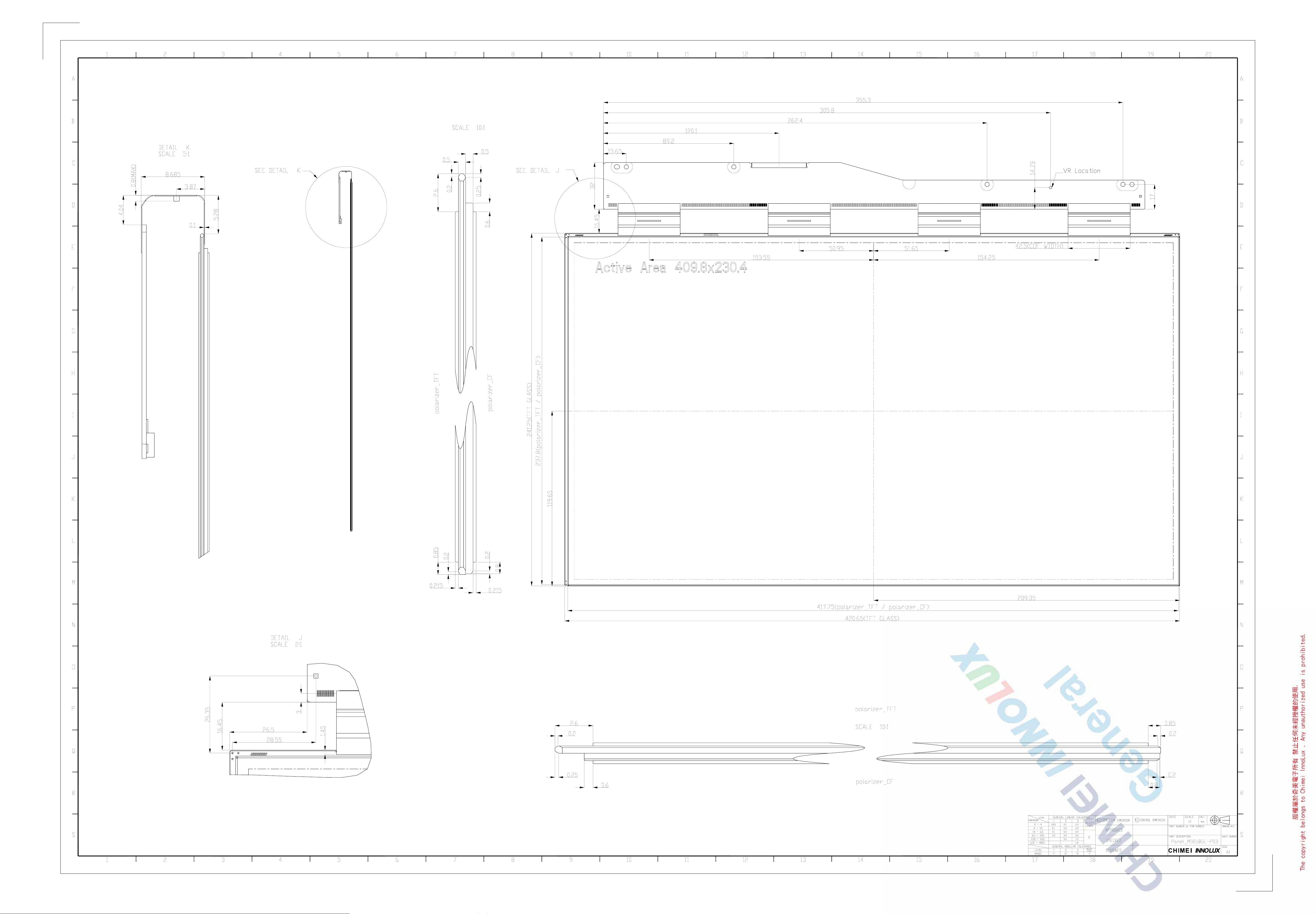
10. OUTLINE DRAWING
Version 3.1 31 MAY 2012 24 / 23
The copyright belongs to CHIMEI InnoLux. Any unauthorized use is prohibited.
Page 24
 Loading...