

Page 1
Global LCD Panel Exchange Center
MODEL NO.: G260JJE
www.panelook.com
PRODUCT SPECIFICATION
Doc. Number :
Ϯ Tentative Specification
ϭ Preliminary Specification
ϭ Approval Specification
SUFFIX: L07
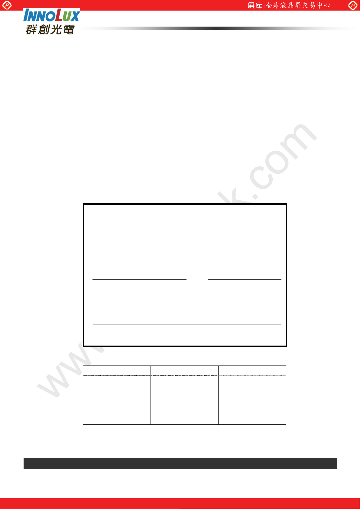
Customer:
APPROVED BY SIGNATURE
Name / Title
Note
Please return 1 copy for your confirmation with your
signature and comments.
Approved By Checked By Prepared By
Version 0.0 JUN 10, 2013 1/27
The copyright belongs to InnoLux. Any unauthorized use is prohibited.
One step solution for LCD / PDP / OLED panel application: Datasheet, inventory and accessory!
www.panelook.com
Page 2
Global LCD Panel Exchange Center
www.panelook.com
PRODUCT SPECIFICATION
- CONTENTS -
REVISION HISTORY ------------------------------------------------------- 3
1. GENERAL DESCRIPTION
1.1 OVERVIEW
1.2 GENERAL SPECIFICATIONS
1.3 MECHANICAL SPECIFICATIONS
------------------------------------------------------- 4
2. ABSOLUTE MAXIMUM RATINGS ------------------------------------------------------- 5
2.1 ABSOLUTE RATINGS OF ENVIRONMENT
2.2 ELECTRICAL ABSOLUTE RATINGS
2.2.1 TFT LCD MODULE
2.2.2 BACKLIGHT UNIT
3. ELECTRICAL CHARACTERISTICS ------------------------------------------------------- 7
3.1 TFT LCD MODULE
3.2 BACKLIGHT UNIT
4. BLOCK DIAGRAM ------------------------------------------------------- 11
4.1 TFT LCD MODULE
4.2 BACKLIGHT UNIT
5. INPUT TERMINAL PIN ASSIGNMENT ------------------------------------------------------- 12
5.1 TFT LCD MODULE
5.2 BACKLIGHT UNIT
5.3 COLOR DATA INPUT ASSIGNMENT
6. INTERFACE TIMING ------------------------------------------------------- 15
6.1 INPUT SIGNAL TIMING SPECIFICATIONS
2 POWER ON/OFF SEQUENCE
6.
6.3 VDD Power DIP Condition
7. OPTICAL CHARACTERISTICS ------------------------------------------------------- 17
7.1 TEST CONDITIONS
7.2 OPTICAL SPECIFICATIONS
8. Reliability Test Criteria ------------------------------------------------------ 21
9. PACKAGING ------------------------------------------------------- 22
9.1 PACKING SPECIFICATIONS
9.2 PACKING METHOD
9.3 UN-PACKING METHOD
10. DEFINITION OF LABELS ------------------------------------------------------- 24
10.1 Innolux MODULE LABEL
11. PRECAUTIONS ------------------------------------------------------- 25
11.1 ASSEMBLY AND HANDLING PRECAUTIONS
11.2 SAFETY PRECAUTIONS
12. MECHANICAL CHARACTERISTICS ------------------------------------------------------- 26
Version 0.0 JUN 10, 2013 2/27
The copyright belongs to InnoLux. Any unauthorized use is prohibited.
One step solution for LCD / PDP / OLED panel application: Datasheet, inventory and accessory!
www.panelook.com
Page 3

Global LCD Panel Exchange Center
www.panelook.com
PRODUCT SPECIFICATION
REVISION HISTORY
Version Date Section Description
0.0 JUN 10, 2013 All G260JJE-L07 Tentative Spec. was first issued.
Version 0.0 JUN 10, 2013 3/27
The copyright belongs to InnoLux. Any unauthorized use is prohibited.
One step solution for LCD / PDP / OLED panel application: Datasheet, inventory and accessory!
www.panelook.com
Page 4
Global LCD Panel Exchange Center
1. GENERAL DESCRIPTION
1.1 OVERVIEW
G260JJE-L06 model is a 25.54” MVA TFT-LCD module with a white LED Backlight Unit and a 30 pins 2
channels LVDS interface. This module supports 1920 x 1200 WUXGA mode and can display up to 16.7
millions colors. The converter for the Backlight Unit is built in.
1.2 GENERAL SPECIFICATIONS
Item Specification Unit Note
Active Area 550.08 (H) x 343.8 (V) (25.54” diagonal) mm
Bezel Opening Area 554.1 (H) x 347.8 (V) mm
Driver Element a-Si TFT active matrix - -
Pixel Number 1920 x R.G.B. x 1200 pixel -
Pixel Pitch 0.2865 (H) x 0.2865 (V) mm -
Pixel Arrangement RGB vertical stripe - -
Display Colors 16.7M color -
Transmissive Mode Normally black - -
Surface Treatment AG type, 3H hard coating, - -
www.panelook.com
PRODUCT SPECIFICATION
(1)
1.3 MECHANICAL SPECIFICATIONS
Item Min. Typ. Max. Unit Note
Horizontal(H) (581.5) (582.0) (582.5) mm
Module Size
Note (1) Please refer to the attached drawings for more information of front and back outline dimensions.
Vertical(V) (375.1) (375.6) (376.1) mm
Depth(D) (29.6) (30.1) (30.6) mm
Weight - (3770) - g -
(1)
Version 0.0 JUN 10, 2013 4/27
The copyright belongs to InnoLux. Any unauthorized use is prohibited.
One step solution for LCD / PDP / OLED panel application: Datasheet, inventory and accessory!
www.panelook.com
Page 5
Global LCD Panel Exchange Center
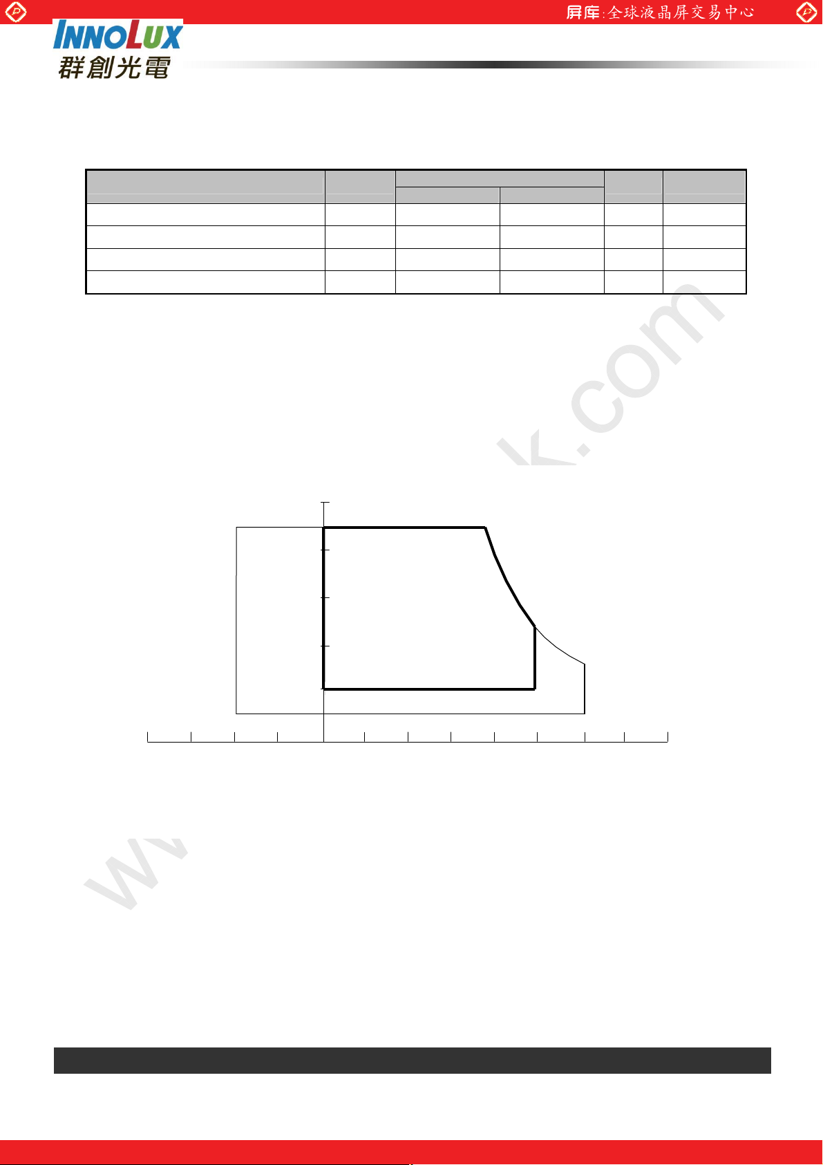
2. ABSOLUTE MAXIMUM RATINGS
2.1 ABSOLUTE RATINGS OF ENVIRONMENT
Item Symbol
Storage Temperature TST (-20) (60) ºC (1)
Operating Ambient Temperature TOP (0) (50) ºC (1), (2)
Shock (Non-Operating) S
Vibration (Non-Operating) V
Note (1) Temperature and relative humidity range is shown in the figure below.
(a) 90 %RH Max. (Ta Љ 40 ºC).
(b) Wet-bulb temperature should be 39 ºC Max. (Ta > 40 ºC).
(c) No condensation.
Note (2) The temperature of panel display surface area should be 0 ºC Min. and 60 ºC Max
www.panelook.com
PRODUCT SPECIFICATION
Valu e
Min. Max.
- (40) G (3), (5)
NOP
- (1.5) G (4), (5)
NOP
Unit Note
Relative Humidity (%RH)
100
90
80
60
Operating Range
40
20
10
Storage Range
Temperature (ºC)
Note (3) 1 time for ± X, ± Y, ± Z. for Condition (25G / 6ms) is half Sine Wave,.
Note (4) 5- 9Hz: 3,5mm amplitude 9- 500Hz: 1g- each 10 cycles / axis (X,Y,Z); 1 octave / min.
80 60 -20 40 0 20 -40
Note (5) At testing Vibration and Shock, the fixture in holding the module has to be hard and rigid
enough so that the module would not be twisted or bent by the fixture.
Version 0.0 JUN 10, 2013 5/27
The copyright belongs to InnoLux. Any unauthorized use is prohibited.
One step solution for LCD / PDP / OLED panel application: Datasheet, inventory and accessory!
www.panelook.com
Page 6
Global LCD Panel Exchange Center
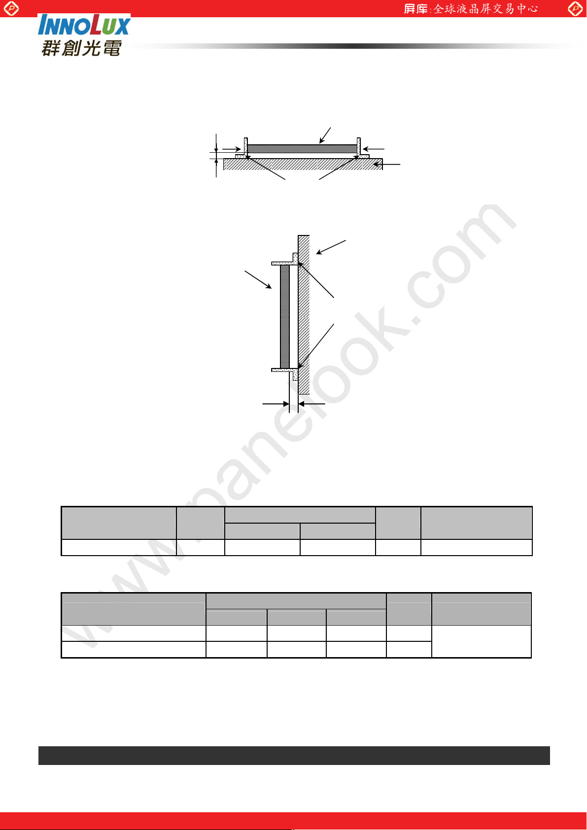
The fixing condition is shown as below:
www.panelook.com
PRODUCT SPECIFICATION
At room Temperature
Side Mount Fixing
LCD Module
Gap=2mm
X Direction
LCD Module
Side Mount Fixing
Stage
Bracket
Stage
Bracket
Gap=2mm
Y Direction
2.2 ELECTRICAL ABSOLUTE RATINGS
2.2.1 TFT LCD MODULE
Item Symbol
Min. Max.
Power Supply Voltage Vcc (-0.3) (+6.0) V (1)
Value
Unit Note
2.2.2 BACKLIGHT UNIT
Item
Min Typ. Max.
LED Light Bar Input voltage - (37.2) (40.8) V
LED Light Bar Input Current - (720) (780) A
Note (1) Permanent damage to the device may occur if maximum values are exceeded. Function
operation should be restricted to the conditions described under Normal Operating Conditions.
Note (2) Specified values are for LED (Refer to Section 3.2 for further information).
Value
Unit Note
DC
DC
(1), (2)
Version 0.0 JUN 10, 2013 6/27
The copyright belongs to InnoLux. Any unauthorized use is prohibited.
One step solution for LCD / PDP / OLED panel application: Datasheet, inventory and accessory!
www.panelook.com
Page 7
Global LCD Panel Exchange Center
www.panelook.com
PRODUCT SPECIFICATION
3. ELECTRICAL CHARACTERISTICS
3.1 TFT LCD MODULE Ta = 25 ± 2 ºC
Parameter Symbol
Min. Typ. Max.
Power Supply Voltage Vcc (4.5) (5.0) (5.50) V -
Ripple Voltage VRP - - (100) mV -
Rush Current I
White - (1.36) (1.9) A (3)a
Power Supply Current
Black - (0.9) (1.26) A (3)b
Vertical Stripe
- - (3.8) A (2)
RUSH
-
-
-
- (1.4) (1.96) A (3)c
LVDS Differential Input High Threshold VTH(LVDS) - - +100 mV Vic=1.2V
LVDS Differential Input Low Threshold VTL(LVDS) (-100) - - mV Vic=1.2V
LVDS differential input voltage Vid (100) - (600) mV
Value
Unit Note
LVDS common input voltage Vic - (1.2) - V
Logic “L” input voltage Vil Vss - (0.8) V
Note (1) The assembly should be always operated within above ranges.
Note (2) Measurement Conditions:
(High to Low)
(Control Signal)
SW
+12V
+5.0V
R1
47K
R2
1K
47K
VR1
C1
1uF
Q1 2SK1475
C2
0.01uF
Q2
2SK1470
FUSE
C3
1uF
Vcc
(LCD Module Input)
Vcc rising time is 470μs
VCC
0.9Vcc
0.1Vcc
GND
470μs
Version 0.0 JUN 10, 2013 7/27
The copyright belongs to InnoLux. Any unauthorized use is prohibited.
One step solution for LCD / PDP / OLED panel application: Datasheet, inventory and accessory!
www.panelook.com
Page 8
Global LCD Panel Exchange Center
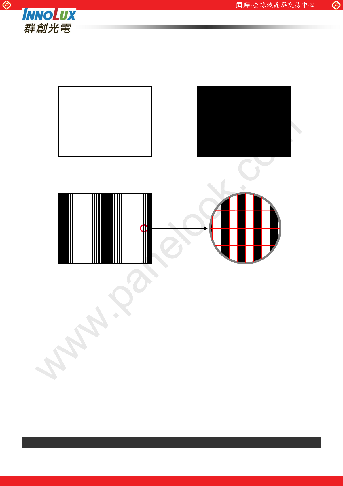
Note (3) The specified power supply current is under the conditions at Vcc = 5.0 V, Ta = 25 ± 2 ºC, fv = 60
Hz, whereas a power dissipation check pattern below is displayed.
www.panelook.com
PRODUCT SPECIFICATION
a. White Pattern
Active Area
c. Vertical Stripe Pattern
b. Black Pattern
Active Area
R
G
R
B
G
R
B
G
B
B
B
R
R
R
G
G
G
B
B
B
R
R
Active Area
R R
G
B
G
B
Version 0.0 JUN 10, 2013 8/27
The copyright belongs to InnoLux. Any unauthorized use is prohibited.
One step solution for LCD / PDP / OLED panel application: Datasheet, inventory and accessory!
www.panelook.com
Page 9
Global LCD Panel Exchange Center
3.2 BACKLIGHT UNIT
www.panelook.com
PRODUCT SPECIFICATION
Ta = 25 ± 2 ºC
Parameter Symbol
Converter Power Supply Voltage Vi (21.6) (24.0) (26.4)
Converter Power Supply Current Ii --- (1.2) (1.5) A
LED Power Consumption PO --- (30) (35) W
EN Control Level
PWM Control Level
PWM Control Duty Ratio (1) (100) %
PWM Control Frequency f
LED Life Time LL (50,000) Hrs (1), (2)
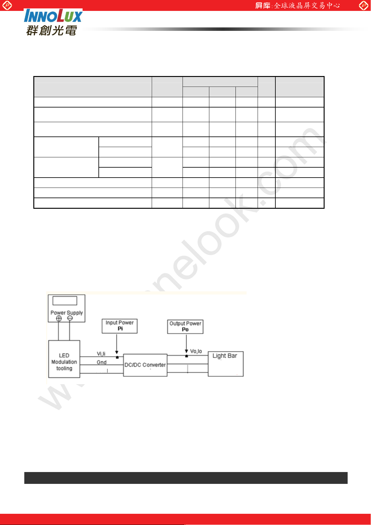
Note (1) LED current is measured by utilizing a high frequency current meter as shown below:
Note (2) The lifetime of LED is defined as the time when it continues to operate under the conditions at
Ta = 50±2 к and I
value.
Note (3) P
= Io ×V
O
Backlight on (2) (3.3) (5.0) V
Backlight off
PWM High Level (2.0) (3.3) (5.0) V
PWM Low Level
= 60mADC(LED forward current) until the brightness becomes 50% of its original Љ
LED
o
EN1,
EN2
PWM1,
PWM2
PWM
Min. Typ. Max.
(0) (0) (0.8) V
(0) (0) (0.8) V
(100) (200) (210) Hz
Valu e
Unit
V
(Duty 100%)
(Duty 100%)
(Duty 100%),(3)
Note
@ Vi = 24V
@ Vi = 24V
EN,_E_PWM
Version 0.0 JUN 10, 2013 9/27
The copyright belongs to InnoLux. Any unauthorized use is prohibited.
One step solution for LCD / PDP / OLED panel application: Datasheet, inventory and accessory!
www.panelook.com
Page 10

Global LCD Panel Exchange Center
www.panelook.com
PRODUCT SPECIFICATION
Power sequence and control signal timing are shown in the following figure
+24V
EN
0
0
Tr<200ms
>50ms
T>=10ms
>10ms
E_PWM
0
Note ΚWhile system is turned ON or OFF, the power sequences must follow as below descriptions:
Turn ON sequence: Vi(+24V) Ш EN Ш E_PWM signal
Turn OFF sequence: E_PWM signal Ш EN Ш Vi(+24V)
INPUT TERMINAL PIN ASSIGNMENT
Pin Name Description
1 Vi Converter Power Supply(+24V)
2 Vi Converter Power Supply(+24V)
3 Vi Converter Power Supply(+24V)
4 Vi Converter Power Supply(+24V)
5 Vi Converter Power Supply(+24V)
6 GND Ground
7 GND Ground
8 GND Ground
9 GND Ground
10 GND Ground
11 NC No connection
12 EN Enable Control (for light Bar)
13 NC No connection
14 E_PWM Dimming Control (for light Bar)
Note (1) Connector Part No.: FCN_JH2-D4-143N.
Version 0.0 JUN 10, 2013 10/27
The copyright belongs to InnoLux. Any unauthorized use is prohibited.
One step solution for LCD / PDP / OLED panel application: Datasheet, inventory and accessory!
www.panelook.com
Page 11

Global LCD Panel Exchange Center
4. BLOCK DIAGRAM
4.1 TFT LCD MODULE
www.panelook.com
PRODUCT SPECIFICATION
RXO0(+/-)
RXO1(+/-)
RXO2(+/-)
RXO3(+/-)
RXOC(+/-)
RXE0(+/-)
RXE1(+/-)
RXE2(+/-)
RXE3(+/-)
RXEC(+/-)
NC
Vcc
GND
VL
(Starconn 093G30B0001A
or JAE FI-X30SSL-HF)
INPUT CONNECTOR
LED Converter
LVDS INPUT /
TIMING CONTROLLER
DC/DC CONVERTER &
REFERENCE VOLTAGE
SCAN DRIVER IC
TFT LCD PANEL
(1920x3x1200)
DATA DRIVER IC
BACKLIGHT UNIT
Version 0.0 JUN 10, 2013 11/27
The copyright belongs to InnoLux. Any unauthorized use is prohibited.
One step solution for LCD / PDP / OLED panel application: Datasheet, inventory and accessory!
www.panelook.com
Page 12

Global LCD Panel Exchange Center
5. INPUT TERMINAL PIN ASSIGNMENT
5.1 TFT LCD MODULE
Pin Name Description
1 RXO0- Negative LVDS differential data input. Channel O0 (odd)
2 RXO0+ Positive LVDS differential data input. Channel O0 (odd)
3 RXO1- Negative LVDS differential data input. Channel O1 (odd)
4 RXO1+ Positive LVDS differential data input. Channel O1 (odd)
5 RXO2- Negative LVDS differential data input. Channel O2 (odd)
6 RXO2+ Positive LVDS differential data input. Channel O2 (odd)
7 GND Ground
8 RXOC- Negative LVDS differential clock input. (odd)
9 RXOC+ Positive LVDS differential clock input. (odd)
10 RXO3- Negative LVDS differential data input. Channel O3(odd)
www.panelook.com
PRODUCT SPECIFICATION
11 RXO3+ Positive LVDS differential data input. Channel O3 (odd)
12 RXE0- Negative LVDS differential data input. Channel E0 (even)
13 RXE0+ Positive LVDS differential data input. Channel E0 (even)
14 GND Ground
15 RXE1- Negative LVDS differential data input. Channel E1 (even)
16 RXE1+ Positive LVDS differential data input. Channel E1 (even)
17 GND Ground
18 RXE2- Negative LVDS differential data input. Channel E2 (even)
19 RXE2+ Positive LVDS differential data input. Channel E2 (even)
20 RXEC- Negative LVDS differential clock input. (even)
21 RXEC+ Positive LVDS differential clock input. (even)
22 RXE3- Negative LVDS differential data input. Channel E3 (even)
23 RXE3+ Positive LVDS differential data input. Channel E3 (even)
24 GND Ground
25 NC No connection, this pin should be opened.
26 NC No connection, this pin should be opened.
27 VCC +5.0V power supply
28 VCC +5.0V power supply
29 VCC +5.0V power supply
30 VCC +5.0V power supply
Note (1) Connector Part No.: P2 187114-30091.
Note (2) The first pixel is odd.
Note (3) Input signal of even and odd clock should be the same timing.
Version 0.0 JUN 10, 2013 12/27
The copyright belongs to InnoLux. Any unauthorized use is prohibited.
One step solution for LCD / PDP / OLED panel application: Datasheet, inventory and accessory!
www.panelook.com
Page 13

Global LCD Panel Exchange Center
5.2 The Input Data Format
www.panelook.com
PRODUCT SPECIFICATION
LVDS Channel O0
LVDS Channel O1
LVDS Channel O2
LVDS Channel O3
LVDS Channel E0
LVDS Channel E1
LVDS Channel E2
LVDS Channel E3
LVDS output D7 D6 D4 D3 D2 D1 D0
Data order OG0 OR5 OR4 OR3 OR2 OR1 OR0
LVDS output D18 D15 D14 D13 D12 D9 D8
Data order OB1 OB0 OG5 OG4 OG3 OG2 OG1
LVDS output D26 D25 D24 D22 D21 D20 D19
Data order DE NA NA OB5 OB4 OB3 OB2
LVDS output D23 D17 D16 D11 D10 D5 D27
Data order NA OB7 OB6 OG7 OG6 OR7 OR6
LVDS output D7 D6 D4 D3 D2 D1 D0
Data order EG0 ER5 ER4 ER3 ER2 ER1 ER0
LVDS output D18 D15 D14 D13 D12 D9 D8
Data order EB1 EB0 EG5 EG4 EG3 EG2 EG1
LVDS output D26 D25 D24 D22 D21 D20 D19
Data order DE NA NA EB5 EB4 EB3 EB2
LVDS output D23 D17 D16 D11 D10 D5 D27
Data order NA EB7 EB6 EG7 EG6 ER7 ER6
Version 0.0 JUN 10, 2013 13/27
The copyright belongs to InnoLux. Any unauthorized use is prohibited.
One step solution for LCD / PDP / OLED panel application: Datasheet, inventory and accessory!
www.panelook.com
Page 14

Global LCD Panel Exchange Center
5.3 COLOR DATA INPUT ASSIGNMENT
The brightness of each primary color (red, green and blue) is based on the 8-bit gray scale data input for
the color. The higher the binary input, the brighter the color. The table below provides the assignment of
color versus data input.
Color
R7 R6 R5 R4 R3 R2 R1 R0 R7 R6 G5 G4 G3 G2 G1 G0 R7 R6 B5 B4 B3 B2 B1 B0
Basic
Colors
Gray
Scale
Of
Red
Black
Red
Green
Blue
Cyan
Magenta
Ye ll ow
White
Red(0) / Dark
Red(1)
Red(2)
:
:
Red(253)
Red(254)
Red(255)
0
0
0
1
1
1
0
0
0
0
0
0
0
0
0
1
1
1
1
1
1
1
1
1
0
0
0
0
0
0
0
0
0
:
:
:
:
:
:
1
1
1
1
1
1
1
1
1
www.panelook.com
PRODUCT SPECIFICATION
Data Signal
Red Green Blue
0
0
0
0
0
0
0
0
0
0
0
0
0
0
0
0
0
1
1
1
1
1
0
0
0
0
0
0
0
0
0
0
0
0
0
0
0
0
0
1
1
1
1
1
1
1
1
0
0
0
0
0
0
0
0
0
0
0
0
0
0
0
0
0
1
1
1
1
0
0
0
0
0
1
1
1
1
1
1
1
1
1
1
1
1
1
1
1
1
1
0
0
0
0
0
0
0
0
1
1
1
1
1
1
1
1
1
1
1
1
1
1
1
1
1
0
0
0
0
1
1
1
1
1
1
1
1
1
1
1
1
1
1
1
1
1
0
0
0
0
0
0
0
0
0
0
0
0
0
0
0
0
0
0
0
0
0
1
0
0
0
0
0
0
0
0
0
0
0
0
0
0
0
1
0
0
0
0
0
0
0
0
0
0
0
0
0
:
:
:
:
:
:
:
:
:
:
:
:
:
:
:
:
:
:
:
:
:
:
:
:
:
:
:
:
:
:
:
:
:
:
1
1
1
0
1
0
0
0
0
0
0
0
0
0
0
0
0
1
1
1
1
0
0
0
0
0
0
0
0
0
0
0
0
0
1
1
1
1
1
0
0
0
0
0
0
0
0
0
0
0
0
0
0
0
0
0
0
0
0
0
0
0
0
1
1
1
1
1
1
1
1
1
1
1
1
0
0
0
0
1
1
1
1
0
0
0
0
0
0
0
0
0
0
0
0
:
:
:
:
:
:
:
:
0
0
0
0
0
0
0
0
0
0
0
0
Green(0) / Dark
Green(1)
Gray
Scale
Of
Green
Gray
Scale
Of
Blue
Note (1) 0: Low Level Voltage, 1: High Level Voltage
Green(2)
:
:
Green(253)
Green(254)
Green(255)
Blue(0) / Dark
Blue(1)
Blue(2)
:
:
Blue(253)
Blue(254)
Blue(255)
0
0
0
0
0
0
0
0
0
0
0
0
0
0
0
0
0
0
0
0
0
:
:
:
:
:
:
:
:
:
:
:
:
:
:
0
0
0
0
0
0
0
0
0
0
0
0
0
0
0
0
0
0
0
0
0
0
0
0
0
0
0
0
0
0
0
0
0
0
0
0
0
0
0
0
0
0
:
:
:
:
:
:
:
:
:
:
:
:
:
:
0
0
0
0
0
0
0
0
0
0
0
0
0
0
0
0
0
0
0
0
0
0
0
0
0
0
0
0
0
0
0
0
0
0
0
0
0
0
0
0
0
0
0
0
0
0
1
0
0
0
0
0
0
0
0
0
0
0
0
0
0
0
1
0
0
0
0
0
0
0
0
0
:
:
:
:
:
:
:
:
:
:
:
:
:
:
:
:
:
:
:
:
:
:
:
:
:
:
:
:
:
:
:
:
:
:
0
1
1
1
1
1
1
0
1
0
0
0
0
0
0
0
0
0
1
1
1
1
1
1
1
0
0
0
0
0
0
0
0
0
0
1
1
1
1
1
1
1
1
0
0
0
0
0
0
0
0
0
0
0
0
0
0
0
0
0
0
0
0
0
0
0
0
0
0
0
0
0
0
0
0
0
0
0
0
0
0
0
0
0
1
0
0
0
0
0
0
0
0
0
0
0
0
0
0
0
1
0
:
:
:
:
:
:
:
:
:
:
:
:
:
:
:
:
:
:
:
:
:
:
:
:
:
:
:
:
:
:
:
:
:
:
0
0
0
0
0
0
0
0
0
1
1
1
1
1
1
0
1
0
0
0
0
0
0
0
0
0
1
1
1
1
1
1
1
0
0
0
0
0
0
0
0
0
0
1
1
1
1
1
1
1
1
Version 0.0 JUN 10, 2013 14/27
The copyright belongs to InnoLux. Any unauthorized use is prohibited.
One step solution for LCD / PDP / OLED panel application: Datasheet, inventory and accessory!
www.panelook.com
Page 15

Global LCD Panel Exchange Center
6. INTERFACE TIMING
6.1 INPUT SIGNAL TIMING SPECIFICATIONS
The input signal timing specifications are shown as the following table and timing diagram.
Signal Item Symbol Min. Typ. Max. Unit Note
Frequency Fc (50.0) (77) (83.0) MHz -
LVDS Clock
LVDS Data
Vertical Active Display Term
Horizontal Active Display Term
Period Tc - (13.0) - ns
High Time Tch - (4/7) - Tc -
Low Time Tcl - (3/7) - Tc -
Setup Time Tlvs (600) - - ps -
Hold Time Tlvh (600) - - ps -
Frame Rate Fr (40) (60) (63) Hz Tv=Tvd+Tvb
Total Tv (1209) (1235) (1245) Th -
Display Tvd (1200) (1200) (1200) Th -
Blank Tvb (9) (35) Tv-Tvd Th -
Total Th (1030) (1040) (1060) Tc Th=Thd+Thb
Display Thd (960) (960) (960) Tc -
Blank Thb (70) (80) Th-Thd Tc -
www.panelook.com
PRODUCT SPECIFICATION
Note: Because this module is operated by DE only mode, Hsync and Vsync input signals should be set
to low logic level or ground. Otherwise, this module would operate abnormally.
INPUT SIGNAL TIMING DIAGRAM
Tv
DE
Th
DCLK
DE
DATA
TC
Thb
hd
T
Version 0.0 JUN 10, 2013 15/27
The copyright belongs to InnoLux. Any unauthorized use is prohibited.
One step solution for LCD / PDP / OLED panel application: Datasheet, inventory and accessory!
www.panelook.com
Page 16

Global LCD Panel Exchange Center
d
www.panelook.com
PRODUCT SPECIFICATION
6.2 POWER ON/OFF SEQUENCE
To prevent a latch-up or DC operation of LCD module, the power on/off sequence should be as the
diagram below.
RestartPower On Power Off
- Power Supply
for LCD, Vcc
- Interface Signal
(LVDS Signal of
Transmitter), V
- Power for LED
Timing Specifications:
0.5< t1 Љ 10 msec
0 < t2 Љ 50 msec
0 < t3 Љ 50 msec
I
t4 Њ 500 msec
t5 Њ 500 msec
0V
0V
10%
90%
90%
10%
t1
t4
t3 t2
Valid Data
t6 t5
50% 50%
ON OFF OFF
t6 Њ 90 msec
6.3 VDD Power DIP Condition
Vcc
4.5V
4.0V
T
Dip condition:
msTdVVccV 20,5.40.4 ≤≤≤
Version 0.0 JUN 10, 2013 16/27
The copyright belongs to InnoLux. Any unauthorized use is prohibited.
One step solution for LCD / PDP / OLED panel application: Datasheet, inventory and accessory!
www.panelook.com
Page 17

Global LCD Panel Exchange Center
7. OPTICAL CHARACTERISTICS
7.1 TEST CONDITIONS
Item Symbol Value Unit
Ambient Temperature Ta
Ambient Humidity Ha
Supply Voltage VCC (5) V
Input Signal According to typical value in "3. ELECTRICAL CHARACTERISTICS"
Converter PWM duty (100%)
7.2 OPTICAL SPECIFICATIONS
The relative measurement methods of optical characteristics are shown in 7.2. The following items
should be measured under the test conditions described in 7.1 and stable environment shown in Note (5).
www.panelook.com
PRODUCT SPECIFICATION
o
(25±2)
(50±10)
C
%RH
Item Symbol Condition Min. Typ . Max. Unit Note
Contrast Ratio CR (1000) (1500) - - (2), (5)
Response Time
Center Luminance of White LC (300) (350) - cd/m2(4), (5)
White Variation
Red
Green
Color
Chromaticity
Blue
White
Horizontal
Viewing Angle
Vertical
TR - (15) - ms
T
- (5) - ms
F
δW
Rx
Ry
Gx
Gy
Bx
By
Wx (0.298) -
Wy
θx+
θx-
θ
=0°,θY=0°
x
Viewing Normal
Angle
CR≥10
θY+
θY-
- (1.4) (1.5) - (5), (6)
(0.638)
(0.342)
(0.310)
Typ.-
0.05
80 88 -
80 88 -
80 88 -
80 88
(0.616)
(0.153)
(0.055)
(0.308)
Typ.+
0.05
-
-
-
-
-
-
-
-
Deg.
(3)
(1),
(5)
(1),
(5)
Version 0.0 JUN 10, 2013 17/27
The copyright belongs to InnoLux. Any unauthorized use is prohibited.
One step solution for LCD / PDP / OLED panel application: Datasheet, inventory and accessory!
www.panelook.com
Page 18

Global LCD Panel Exchange Center
T
Note (1) Definition of Viewing Angle (θx, θy):
www.panelook.com
PRODUCT SPECIFICATION
Normal
θx = θy = 0º
θy- θy+
θX- = 90º
6 o’clock
θ
y- = 90º
x-
y-
Note (2) Definition of Contrast Ratio (CR):
The contrast ratio can be calculated by the following expression.
Contrast Ratio (CR) = L255 / L0
L255: Luminance of gray level 255
L 0: Luminance of gray level 0
CR = CR (5)
θx−
θx+
y+
12 o’clock direction
θ
y+ = 90º
x+
θX+ = 90º
CR (X) is corresponding to the Contrast Ratio of the point X at Figure in Note (6).
Note (3) Definition of Response Time (T
Gray Level 255
100%
90%
Optical
Response
10%
0%
, TF) and measurement method:
R
Gray Level 0
T
F T
Gray Level 255
ime
R
Version 0.0 JUN 10, 2013 18/27
The copyright belongs to InnoLux. Any unauthorized use is prohibited.
One step solution for LCD / PDP / OLED panel application: Datasheet, inventory and accessory!
www.panelook.com
Page 19

Global LCD Panel Exchange Center
Note (4) Definition of Luminance of White (LC):
www.panelook.com
PRODUCT SPECIFICATION
L
Note (5) Measurement Setup:
= L (1), where L (X) is corresponding to the luminance of the point X at the figure in Note (6)
C
The LCD module should be stabilized at given temperature for 20 minutes to avoid abrupt
temperature change during measuring. In order to stabilize the luminance, the measurement
should be executed after lighting Backlight for 20 minutes in a windless room.
LCD Module
LCD Panel
USB2000
Center of the Screen
500 mm
CS-1000T
Light Shield Room
(Ambient Luminance < 2 lux)
Version 0.0 JUN 10, 2013 19/27
The copyright belongs to InnoLux. Any unauthorized use is prohibited.
One step solution for LCD / PDP / OLED panel application: Datasheet, inventory and accessory!
www.panelook.com
Page 20

Global LCD Panel Exchange Center
Note (6) Definition of White Variation (δW):
Measure the luminance of gray level 255 at 13 points
www.panelook.com
PRODUCT SPECIFICATION
δW =
Maximum [L (1), L (2), L (3), L (4), L (5),L (6),L (7),L (8),L (9),L (10),L (11),L (12),L (13)]
Minimum [L (1), L (2), L (3), L (4), L (5) ,L (6),L (7),L (8),L (9),L (10),L (11),L (12),L (13)]
˄˃
ˊ
˄
˄˅
˗
˩˸˼˶˴˿ʳ˟˼˸
ˉ
˪˂ˇ
˅
˪˂ˇ
˄˃
ˌ
ˇ
˄˄
˄˃
˗˂ˇ
˗˂ˇ
˪
˪˂ˇ˪˂ˇ
˛ ˼ ˴ ˿ʳ˟ ˼˸
Active Area
˗˂ˇ
ˋ
ˆ
˄˃
ˈ
˄ˆ
˄˃
˗˂ˇ
ˍʳ˧˸ʳˣ˼
˫
˫ː˄ʳʳ˄ˆ
Version 0.0 JUN 10, 2013 20/27
The copyright belongs to InnoLux. Any unauthorized use is prohibited.
One step solution for LCD / PDP / OLED panel application: Datasheet, inventory and accessory!
www.panelook.com
Page 21

Global LCD Panel Exchange Center
www.panelook.com
PRODUCT SPECIFICATION
8. Reliability Test Criteria
Test Item Test Condition Note
High Temperature Storage Test (60ºC,240 hours)
Low Temperature Storage Test (-20ºC, 240 hours)
Thermal Shock Storage Test (-20ºC, 0.5hour←→60 ºC, 0.5hour; 1hour/cycle,100cycles)
High Temperature Operation Test (50ºC, 240 hours)
Low Temperature Operation Test (-0ºC, 240 hours)
High Temperature & High Humidity
Operation Test
Shock (Non-Operating) (40g, half sine, duration: 11ms,1times for ±X, ±Y, ±Z) (3)(4)
(50ºC,80%RH, 240hours)
(1)(2)(4)
Vibration (Non-Operating)
Note (1) There should be no condensation on the surface of panel during test.
Note (2) Temperature of panel display surface area should be 70 ºC Max.
Note (3) At testing Vibration and Shock, the fixture in holding the module has to be hard and rigid enough so
that the module would not be twisted or bent by the fixture.
Note (4) In the standard conditions, there is no function failure issue occurred. All the cosmetic specification
is judged before reliability test.
(fЈ10Д300Hz, 1.5G, 10min/cycles,3cycles each X, Y, Z,)
(3)(4)
Version 0.0 JUN 10, 2013 21/27
The copyright belongs to InnoLux. Any unauthorized use is prohibited.
One step solution for LCD / PDP / OLED panel application: Datasheet, inventory and accessory!
www.panelook.com
Page 22

Global LCD Panel Exchange Center
9. PACKAGING
9.1 PACKING SPECIFICATIONS
(1) 5 LCD modules / 1 Box
(2) Box dimensions: 713(L)x429(W)x453(H)mm
(3) Weight: approximately 21.1Kg (5 modules per box)
9.2 PACKING METHOD
(1) Carton Packing should have no failure in the following reliability test items.
Test Item Test Conditions Note
ISTA STANDARD
Random, Frequency Range: 1 – 200 Hz
Vibration
Top & Bottom: 30 minutes (+Z), 10 min (-Z),
Right & Left: 10 minutes (X)
Back & Forth 10 minutes (Y)
www.panelook.com
PRODUCT SPECIFICATION
Non Operation
Dropping Test 1 Angle, 3 Edge, 6 Face, 60cm Non Operation
Figure. 9-1 Packing method
Version 0.0 JUN 10, 2013 22/27
The copyright belongs to InnoLux. Any unauthorized use is prohibited.
One step solution for LCD / PDP / OLED panel application: Datasheet, inventory and accessory!
www.panelook.com
Page 23

Global LCD Panel Exchange Center
www.panelook.com
PRODUCT SPECIFICATION
9.3 UN-PACKING METHOD
Figure. 9-2 Packing method
Version 0.0 JUN 10, 2013 23/27
The copyright belongs to InnoLux. Any unauthorized use is prohibited.
One step solution for LCD / PDP / OLED panel application: Datasheet, inventory and accessory!
www.panelook.com
Page 24

Global LCD Panel Exchange Center
www.panelook.com
PRODUCT SPECIFICATION
10. DEFINITION OF LABELS
10.1 Innolux MODULE LABEL
The barcode nameplate is pasted on each module as illustration, and its definitions are as following explanation.
G260JJE -L07 Rev.XX
X X X X X X X Y M D L N N N N
(a) Model Name: G260JJE -L07
(b) Revision: Rev. XX, for example: A1, B1,C1, C2 …etc.
(c) Serial ID: X X
X X X X X Y M D X N N N N
Serial No.
InnoLux Internal Use
Year, Month, Date
InnoLux Internal Use
Revision
InnoLux Internal Use
E207943
MADE IN TAIWAN
ϿϿϿϿ
RoHS
Serial ID includes the information as below:
(a) Manufactured Date: Year: 1~9, for 2011~2019
Month: 1~9, A~C, for Jan. ~ Dec.
Day: 1~9, A~Y, for 1
(b) Revision Code: cover all the change
(c) Serial No.: Manufacturing sequence of product
st
to 31st, exclude I , O and U
Version 0.0 JUN 10, 2013 24/27
The copyright belongs to InnoLux. Any unauthorized use is prohibited.
One step solution for LCD / PDP / OLED panel application: Datasheet, inventory and accessory!
www.panelook.com
Page 25

Global LCD Panel Exchange Center
www.panelook.com
PRODUCT SPECIFICATION
11. PRECAUTIONS
11.1 ASSEMBLY AND HANDLING PRECAUTIONS
(1) Do not apply rough force such as bending or twisting to the module during assembly.
(2) To assemble or install module into user’s system can be only in clean working areas. The dust and oil
may cause electrical short or worsen the polarizer.
(3) It’s not permitted to have pressure or impulse on the module because the LCD panel and Backlight
will be damaged.
(4) Always follow the correct power sequence when LCD module is connecting and operating. This can
prevent damage to the CMOS LSI chips during latch-up.
(5) Do not pull the I/F connector in or out while the module is operating.
(6) Do not disassemble the module.
(7) Use a soft dry cloth without chemicals for cleaning, because the surface of polarizer is very soft and
easily scratched.
(8) It is dangerous that moisture come into or contacted the LCD module, because moisture may damage
LCD module when it is operating.
(9) High temperature or humidity may reduce the performance of module. Please store LCD module
within the specified storage conditions.
(10) When ambient temperature is lower than 10ºC may reduce the display quality. For example, the
response time will become slowly, and the starting voltage of backlight will be higher than room
temperature.
(11) Do not keep same pattern in a long period of time. It may cause image sticking on LCD.
11.2 SAFETY PRECAUTIONS
(1) Do not disassemble the module or insert anything into the Backlight unit.
(2) If the liquid crystal material leaks from the panel, it should be kept away from the eyes or mouth. In
case of contact with hands, skin or clothes, it has to be washed away thoroughly with soap.
(3) After the module’s end of life, it is not harmful in case of normal operation and storage.
Version 0.0 JUN 10, 2013 25/27
The copyright belongs to InnoLux. Any unauthorized use is prohibited.
One step solution for LCD / PDP / OLED panel application: Datasheet, inventory and accessory!
www.panelook.com
Page 26

Global LCD Panel Exchange Center
12. MECHANICAL CHARACTERISTICS
www.panelook.com
PRODUCT SPECIFICATION
Version 0.0 JUN 10, 2013 26/27
The copyright belongs to InnoLux. Any unauthorized use is prohibited.
One step solution for LCD / PDP / OLED panel application: Datasheet, inventory and accessory!
www.panelook.com
Page 27

Global LCD Panel Exchange Center
www.panelook.com
PRODUCT SPECIFICATION
Version 0.0 JUN 10, 2013 27/27
The copyright belongs to InnoLux. Any unauthorized use is prohibited.
One step solution for LCD / PDP / OLED panel application: Datasheet, inventory and accessory!
www.panelook.com
 Loading...