

Page 1
Global LCD Panel Exchange Center
MODEL NO.: G133IGE
www.panelook.com
PRODUCT SPECIFICATION
Doc. Number :
□ Tentative Specification
□ Preliminary Specification
■ Approval Specification
SUFFIX: L03
Customer:
APPROVED BY SIGNATURE
Name / Title
Note
Please return 1 copy for your confirmation with your
signature and comments.
Approved By Checked By Prepared By
yuhsiang.chang
(്/514-10922)
clark.kuo
(ພᤪ/514-10921)
(႓堚ព/514-10920)
archers.huang
2012-03-19
16:24:32 CST
Version 2.0 8 February 2012 1 / 27
The copyright belongs to CHIMEI InnoLux. Any unauthorized use is prohibited.
One step solution for LCD / PDP / OLED panel application: Datasheet, inventory and accessory!
2012-02-21
14:27:06 CST
2012-02-21
14:21:37 CST
www.panelook.com
Page 2
Global LCD Panel Exchange Center
www.panelook.com
PRODUCT SPECIFICATION
- CONTENTS -
REVISION HISTORY
1. GENERAL DESCRIPTION
1.1 OVERVIEW
1.2 FEATURES
1.3 APPLICATION
1.4 GENERAL SPECIFICATIONS
1.5 MECHANICAL SPECIFICATIONS
2. ABSOLUTE MAXIMUM RATINGS
2.1 ABSOLUTE RATINGS OF ENVIRONMENT
2.2 ELECTRICAL ABSOLUTE RATINGS
2.2.1 TFT LCD MODULE
2.2.2 LED CONVERTER
3. ELECTRICAL CHARACTERISTICS
3.1 RECOMMENDED OPERATIN CONDITION
3.2 BACKLIGHT UNIT
4. BLOCK DIAGRAM
4.1 TFT LCD MODULE
5. INPUT TERMINAL PIN ASSIGNMENT
5.1 LVDS I/O PIN ASSIGNMENT
5.2 BACKLIGHT PIN ASSIGNMENT
5.3 TIMING DIAGRAM OF LVDS INPUT SIGNAL
5.4 COLOR DATA INPUT ASSIGNMENT
-------------------------------------------------------
-------------------------------------------------------
-------------------------------------------------------
-------------------------------------------------------
-------------------------------------------------------
-------------------------------------------------------
3
4
6
8
11
12
6. INTERFACE TIMING
6.1 TIMING CHARACTERISTICS
6.2 POWER ON/OFF SEQUENCE
7. OPTICAL CHARACTERISTICS
7.1 TEST CONDITIONS
7.2 OPTICAL SPECIFICATIONS
8. RELIABILITY TEST
8.1RELIABILITY TEST CONDITION
9. PACKAGING
9.1 PACKING SPECIFICATION
9.2 PACKING METHOD
10. DEFINTION OF LABEL
10.1 CMI MODULE LABEL
-------------------------------------------------------
11. PRECAUTIONS
11.1 ASSEMBLY AND HANDLING PRECAUTIONS
11.2 SAFETY PRECAUTIONS
-------------------------------------------------------
-------------------------------------------------------
-------------------------------------------------------
-------------------------------------------------------
--------------------------------------------------------
16
18
21
22
24
25
12. MECHANICAL CHARACTERISTICS
-------------------------------------------------------
Version 2.0 8 February 2012 2 / 27
The copyright belongs to CHIMEI InnoLux. Any unauthorized use is prohibited.
One step solution for LCD / PDP / OLED panel application: Datasheet, inventory and accessory!
26
www.panelook.com
Page 3

Global LCD Panel Exchange Center
www.panelook.com
PRODUCT SPECIFICATION
REVISION HISTORY
Version Date Section Description
Ver 2.0 Feb. 8, ‘11 All G133IGE-L03 Approval specification was first issued.
Version 2.0 8 February 2012 3 / 27
The copyright belongs to CHIMEI InnoLux. Any unauthorized use is prohibited.
One step solution for LCD / PDP / OLED panel application: Datasheet, inventory and accessory!
www.panelook.com
Page 4
Global LCD Panel Exchange Center
1. GENERAL DESCRIPTION
1.1 OVERVIEW
G133IGE-L03 is a 13.3” TFT Liquid Crystal Display module and 20 pins LVDS interface. This module
supports 1280 x 800 WXGA mode and can display 262K or 16.2M colors. The converter circuit for LED
is built in.
1.2 FEATURES
- WXGA (1280 x 800 pixels) resolution
- LVDS (Low Voltage Differential Signaling) interface
- LED light source
www.panelook.com
PRODUCT SPECIFICATION
1.3 APPLICATION
- Industry Application
1.4 GENERAL SPECIFICATI0NS
Item Specification Unit Note
Diagonal Size 13.3 inch
Active Area 286.08 x 178.8 mm
Bezel Opening Area 289.1 x 181.8 mm
Driver Element a-si TFT active matrix - Pixel Number 1280 x R.G.B. x 800 pixel Pixel Pitch 0.2235 x 0.2235 mm Pixel Arrangement RGB vertical stripe - (2)
Display Colors 262k or 16.2M color -
Display Mode Normally White - Surface Treatment Anti-glare, Hard Coating ( 3H ) - Module Power Consumption 6.9 W Typ.
Note (1) Please refer to the attached drawings for more information of front and back outline dimensions.
Note (2)
(1)
Version 2.0 8 February 2012 4 / 27
The copyright belongs to CHIMEI InnoLux. Any unauthorized use is prohibited.
One step solution for LCD / PDP / OLED panel application: Datasheet, inventory and accessory!
www.panelook.com
Page 5
Global LCD Panel Exchange Center
1.5 MECHANICAL SPECIFICATIONS
Item Min. Typ. Max. Unit Note
Horizontal (H) 298.5 299 299.5 mm
Module Size
Note (1) Please refer to the attached drawings for more information of front and back outline dimensions.
Vertical (V) 194.5 195 195.5 mm
Depth (D) - 7.4 7.9 mm
Weight - 382 397 g
www.panelook.com
PRODUCT SPECIFICATION
(1)
Version 2.0 8 February 2012 5 / 27
The copyright belongs to CHIMEI InnoLux. Any unauthorized use is prohibited.
One step solution for LCD / PDP / OLED panel application: Datasheet, inventory and accessory!
www.panelook.com
Page 6
Global LCD Panel Exchange Center
2. ABSOLUTE MAXIMUM RATINGS
2.1 ABSOLUTE RATINGS OF ENVIRONMENT
Item Symbol
Operating Ambient Temperature TOP -30 +70 ºC
Storage Temperature TST -30 +80 ºC
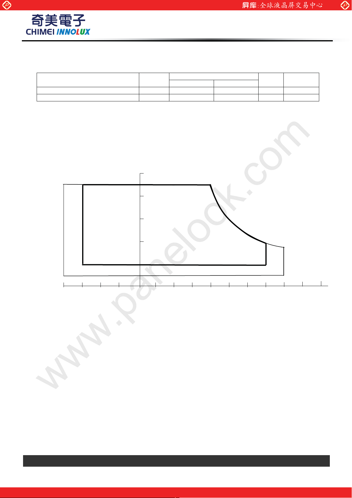
Note (1) Temperature and relative humidity range is shown in the figure below.
(2) Wet-bulb temperature should be 39 ºC Max. (Ta > 40 ºC).
(3) No condensation.
Relative Humidity (%RH)
100
www.panelook.com
PRODUCT SPECIFICATION
Value
Min. Max.
Unit Note
-40
80
60
40
20
Operating Range
Storage Range
Temperature (ºC)
80 60 -20 40 0 20
100
Version 2.0 8 February 2012 6 / 27
The copyright belongs to CHIMEI InnoLux. Any unauthorized use is prohibited.
One step solution for LCD / PDP / OLED panel application: Datasheet, inventory and accessory!
www.panelook.com
Page 7
Global LCD Panel Exchange Center
2.2 ELECTRICAL ABSOLUTE RATINGS
www.panelook.com
PRODUCT SPECIFICATION
2.2.1 TFT LCD MODULE
Item Symbol
Power Supply Voltage Vcc -0.3 4 V (1)
Value
Min. Max.
Unit Note
Ta = 25 ± 2 ºC
2.2.2 LED CONVERTER
Item Symbol
Converter Voltage Vi 4.5 24 V (1) , (2)
Enable Voltage EN --- 5.5 V
Backlight Adjust ADJ --- 5.5 V
Note (1) Permanent damage to the device may occur if maximum values are exceeded. Function operation
should be restricted to the conditions described under Normal Operating Conditions.
Note (2) Specified values are for LED converter (Refer to 3.2 for further information).
Min. Max.
Value
Unit Note
Version 2.0 8 February 2012 7 / 27
The copyright belongs to CHIMEI InnoLux. Any unauthorized use is prohibited.
One step solution for LCD / PDP / OLED panel application: Datasheet, inventory and accessory!
www.panelook.com
Page 8
Global LCD Panel Exchange Center
3. ELECTRICAL CHARACTERISTICS
www.panelook.com
PRODUCT SPECIFICATION
3.1 RECOMMENDED OPERATION CONDITION
Parameter Symbol
Min. Typ. Max.
Ta = 25 ± 2 ºC
Value
Unit Note
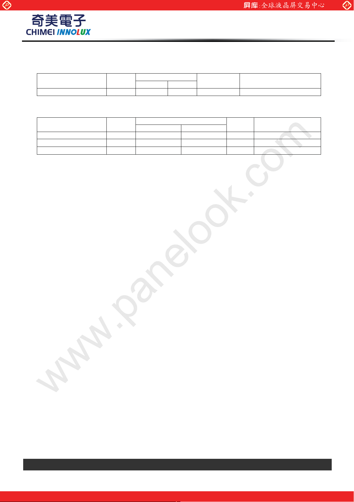
Power Supply Voltage Vcc 3.0 3.3 3.6 V Permissive Ripple Voltage VRP 50 mV Rush Current I
1.5 A (2)
RUSH
Initial Stage Current IIS 1.0 A (2)
Power Supply Current
LVDS Differential Input High Threshold V
LVDS Differential Input Low Threshold V
White 330 370 mA (3)a
Black
Icc
TH(LVDS)
TL(LVDS)
450 490 mA (3)b
100 mV
-100 mV
V
V
(4),
=1.2V
CM
(4)
=1.2V
CM
LVDS Common Mode Voltage VCM 0.7 2.0 V (4)
LVDS Differential Input Voltage |VID| 100 600 mV (4)
Terminating Resistor RT 100 Ohm
Note (1) The assembly should be always operated within above ranges.
Note (2) Measurement Conditions:
Vcc
R1
47K
Q1 2SK1475
FUSE
C3
1uF
Vcc
(LCD Module Input)
(High to Low)
(Control Signal)
SW
+12V
GND
R2
1K
47K
VR1
C1
1uF
0.01uF
Q2
2SK1470
C2
Vcc rising time is 470μs
Vcc
0.9Vcc
0.1Vcc
470μs
Version 2.0 8 February 2012 8 / 27
The copyright belongs to CHIMEI InnoLux. Any unauthorized use is prohibited.
One step solution for LCD / PDP / OLED panel application: Datasheet, inventory and accessory!
www.panelook.com
Page 9

Global LCD Panel Exchange Center
|
|
|
|
Note (3) The specified power supply current is under the conditions at Vcc = 3.3V , Ta = 25 ± 2 ºC, fv = 60
Hz, whereas a power dissipation check pattern below is displayed.
www.panelook.com
PRODUCT SPECIFICATION
a. White Pattern
Active Area
Note (4) The parameters of LVDS signals are defined as the following figures.
CM
V
b. Black Pattern
Active Area
V
Single Ended
ID
Differential
0V
V
V
0V
V
ID
Version 2.0 8 February 2012 9 / 27
The copyright belongs to CHIMEI InnoLux. Any unauthorized use is prohibited.
One step solution for LCD / PDP / OLED panel application: Datasheet, inventory and accessory!
www.panelook.com
Page 10

Global LCD Panel Exchange Center
www.panelook.com
PRODUCT SPECIFICATION
3.2 BACKLIGHT UNIT
Parameter Symbol
Converter Power Supply Voltage Vi
Converter Power Supply Current Ii 0.35 0.45 0.55 A
Converter Power Consumption P
EN Control Level
PWM Control Level
PWM Control Duty Ratio
PWM Control Frequency f
LED Life Time LL 30,000 Hrs (2)
Note (1) LED current is measured by utilizing a high frequency current meter as shown below:
Note (2) The lifetime of LED is defined as the time when it continues to operate under the conditions at
Ta = 25 ±2 к and I
original value.
Note (3) Please note that LED life will be shorter than the average life described in the specification if
operate in higher ambient temperature.
Backlight on 1.6 --- 5 V
Backlight off 0 --- 1 V
PWM High Level 1.3 --- 5 V
PWM Low Level 0 --- 0.65 V
= 18mADC(LED forward current) until the brightness becomes 50% of Љ its
LED
LED
PWM
Min. Typ. Max.
10.8 12.0 13.2 V
--- 5.4 --- W
10 100 %
100 200 20K Hz
Value
Ta = 25 ± 2 ºC
Unit Note
@ Vi = 12V
(Duty 100%)
@ Vi = 12V
(Duty 100%)
Power Supply
Input Power
Vi, Ii
GND
Pi
Converter
LED
Backlight
Unit
Version 2.0 8 February 2012 10 / 27
The copyright belongs to CHIMEI InnoLux. Any unauthorized use is prohibited.
One step solution for LCD / PDP / OLED panel application: Datasheet, inventory and accessory!
www.panelook.com
Page 11

Global LCD Panel Exchange Center
A
4. BLOCK DIAGRAM
4.1 TFT LCD MODULE
FRC
RX3(+/-)
RX0(+/-)
RX1(+/-)
RX2(+/-)
CLK(+/-)
(HIROSE-DF19KR-20P-1H)
INPUT CONNECTOR
www.panelook.com
PRODUCT SPECIFICATION
LVDS INPUT /
TIMING CONTROLLER
SCAN DRIVER IC
TFT LCD PANEL
(1280x R.G.B.x800)
VCC_IN
GND
V
i
DC/DC CONVERTER &
REFERENCE VOLTAGE
CONVERTER CONNECTOR
(E&T 3808K-F05N-03L)
LED
Converter
DAT
DRIVER IC
LED BACKLIGHT
UNIT
Version 2.0 8 February 2012 11 / 27
The copyright belongs to CHIMEI InnoLux. Any unauthorized use is prohibited.
One step solution for LCD / PDP / OLED panel application: Datasheet, inventory and accessory!
www.panelook.com
Page 12

Global LCD Panel Exchange Center
5. INPUT TERMINAL PIN ASSIGNMENT
5.1 LVDS I/O PIN ASSIGNMENT
Pin Symbol Description Polarity Remark
1 Vss Ground
2 Vcc Power Supply +3.3 V (typical)
3 Vcc Power Supply +3.3 V (typical)
4 NC Non-Connection
Dithering control setting
When FRC=H, the width of data input 8 bits
5 FRC
6 Rxin3- LVDS Differential Data Input Negative
7 Rxin3+ LVDS Differential Data Input Positive
8 Rxin0- LVDS Differential Data Input Negative
9 Rxin0+ LVDS Differential Data Input Positive
10 Vss Ground
11 Rxin1- LVDS Differential Data Input Negative
12 Rxin1+ LVDS Differential Data Input Positive
13 Vss Ground
14 Rxin2- LVDS Differential Data Input Negative
15 Rxin2+ LVDS Differential Data Input Positive
16 Vss Ground
17 CLK- LVDS Clock Data Input Negative
18 CLK+ LVDS Clock Data Input Positive
19 Vss Ground
20 Vss Ground
Note (1) User’s connector Part No.: DF19G-20S-1SD (HIROSE) or equivalent DF19G-20S-1For
When FRC=L, the width of data input 6 bits
and set Dx0 and Dx1 to logical low (Default
is L)
www.panelook.com
PRODUCT SPECIFICATION
H is 3.3V
L is GND
LVDS Level Clock
DF19G-20S-1C
5.2 BACKLIGHT PIN ASSIGNMENT (Converter connector pin)
Pin Symbol Description Remark
1 Vi Converter input voltage 12V
2 VGND Converter ground Ground
3 EN Enable pin 3.3V
4 ADJ Backlight Adjust
5 NC Not Connect Ground
Note (1) User’s connector Part No: E&T H208K-P05N-02B or equivalent
PWM Dimming
(Hi: 3.3VDC, Lo: 0VDC)
Version 2.0 8 February 2012 12 / 27
The copyright belongs to CHIMEI InnoLux. Any unauthorized use is prohibited.
One step solution for LCD / PDP / OLED panel application: Datasheet, inventory and accessory!
www.panelook.com
Page 13

Global LCD Panel Exchange Center
5.3 TIMING DIAGRAM OF LVDS INPUT SIGNAL
www.panelook.com
PRODUCT SPECIFICATION
Version 2.0 8 February 2012 13 / 27
The copyright belongs to CHIMEI InnoLux. Any unauthorized use is prohibited.
One step solution for LCD / PDP / OLED panel application: Datasheet, inventory and accessory!
www.panelook.com
Page 14

Global LCD Panel Exchange Center
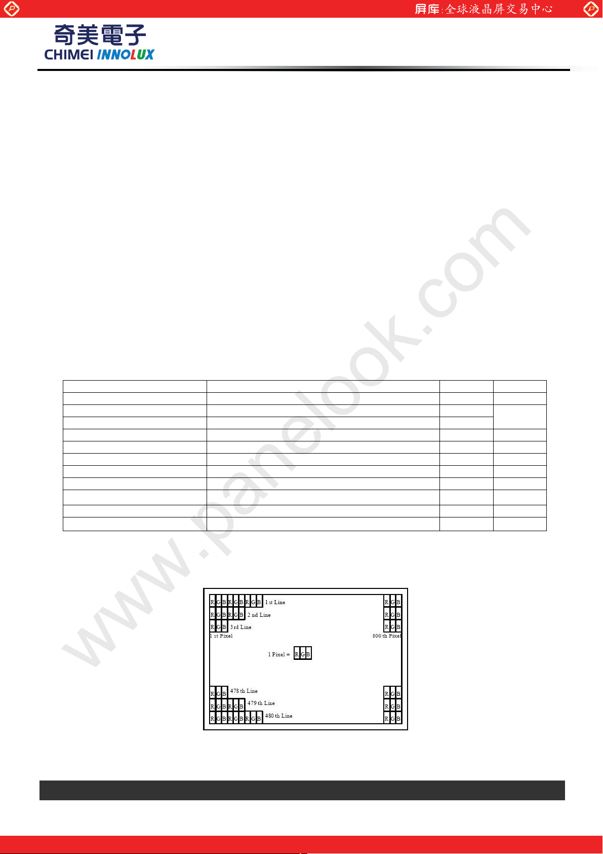
5.4 COLOR DATA INPUT ASSIGNMENT
The brightness of each primary color (red, green and blue) is based on the 6-bit gray scale data input for
the color. The higher the binary input, the brighter the color. The table below provides the assignment of
color versus data input. ( 0: Low Level Voltage, 1: High Level Voltage)
Color
R5 R4 R3 R2 R1 R0 G5 G4 G3 G2 G1 G0 B5 B4 B3 B2 B1 B0
Basic
Colors
Black
Red
Green
Blue
Cyan
Magenta
Ye ll ow
White
0
1
0
0
0
1
1
1
www.panelook.com
PRODUCT SPECIFICATION
Data Signal
Red Green Blue
0
0
0
0
0
0
0
0
0
0
0
0
0
0
0
0
0
1
1
1
1
1
0
0
0
0
0
0
0
0
0
0
0
0
0
0
0
0
0
1
1
1
1
1
1
0
0
0
0
0
0
0
0
0
0
0
0
0
0
0
0
0
1
1
1
1
1
1
0
0
0
0
0
1
1
1
1
1
1
1
1
1
1
1
1
1
1
1
1
1
0
0
0
0
0
0
1
1
1
1
1
1
1
1
1
1
1
1
1
1
1
1
1
0
0
0
0
0
0
1
1
1
1
1
1
1
1
1
1
1
1
1
1
1
1
1
Gray
Scale
Of
Red
Gray
Scale
Of
Green
Gray
Scale
Of
Blue
Red(0) / Dark
Red(1)
Red(2)
:
:
Red(61)
Red(62)
Red(63)
Green(0) / Dark
Green(1)
Green(2)
:
:
Green(61)
Green(62)
Green(63)
Blue(0) / Dark
Blue(1)
Blue(2)
:
:
Blue(61)
Blue(62)
Blue(63)
0
0
0
0
0
0
0
0
0
0
0
0
0
0
0
0
0
0
0
0
0
0
0
1
0
0
0
0
0
0
0
0
0
0
0
0
0
0
0
0
1
0
0
0
0
0
0
0
0
0
0
0
0
0
:
:
:
:
:
:
:
:
:
:
:
:
:
:
:
:
:
:
:
:
:
:
:
:
:
:
:
:
:
:
:
:
:
:
:
:
1
1
1
1
0
1
0
0
0
0
0
0
0
0
0
0
0
0
1
1
1
1
1
0
0
0
0
0
0
0
0
0
0
0
0
0
1
1
1
1
1
1
0
0
0
0
0
0
0
0
0
0
0
0
0
0
0
0
0
0
0
0
0
0
0
0
0
0
0
0
0
0
0
0
0
0
0
0
0
0
0
0
0
1
0
0
0
0
0
0
0
0
0
0
0
0
0
0
0
0
1
0
0
0
0
0
0
0
:
:
:
:
:
:
:
:
:
:
:
:
:
:
:
:
:
:
:
:
:
:
:
:
:
:
:
:
:
:
:
:
:
:
:
:
0
0
0
0
0
0
1
1
1
1
0
1
0
0
0
0
0
0
0
0
0
0
0
0
1
1
1
1
1
0
0
0
0
0
0
0
0
0
0
0
0
0
1
1
1
1
1
1
0
0
0
0
0
0
0
0
0
0
0
0
0
0
0
0
0
0
0
0
0
0
0
0
0
0
0
0
0
0
0
0
0
0
0
0
0
0
0
0
0
1
0
0
0
0
0
0
0
0
0
0
0
0
0
0
0
0
1
0
:
:
:
:
:
:
:
:
:
:
:
:
:
:
:
:
:
:
:
:
:
:
:
:
:
:
:
:
:
:
:
:
:
:
:
:
0
0
0
0
0
0
0
0
0
0
0
0
1
1
1
1
0
1
0
0
0
0
0
0
0
0
0
0
0
0
1
1
1
1
1
0
0
0
0
0
0
0
0
0
0
0
0
0
1
1
1
1
1
1
Version 2.0 8 February 2012 14 / 27
The copyright belongs to CHIMEI InnoLux. Any unauthorized use is prohibited.
One step solution for LCD / PDP / OLED panel application: Datasheet, inventory and accessory!
www.panelook.com
Page 15

Global LCD Panel Exchange Center
www.panelook.com
PRODUCT SPECIFICATION
The brightness of each primary color (red, green and blue) is based on the 8-bit gray scale data input for the color.
The higher the binary input, the brighter the color. The table below provides the assignment of color versus data input.
( 0: Low Level Voltage, 1: High Level Voltage)
Data Signal
Red Green Blue
0
0
0
0
0
0
0
0
0
0
0
0
0
0
0
0
0
0
0
0
0
0
1
1
1
1
1
1
0
0
0
0
0
0
0
0
0
0
0
0
0
0
0
0
0
0
0
0
0
0
1
1
1
1
1
1
1
1
0
0
0
0
0
0
0
0
0
0
0
0
0
0
0
0
0
0
0
0
0
0
1
1
1
1
1
1
1
1
0
0
0
0
0
0
1
1
1
1
1
1
1
1
1
1
1
1
1
1
1
1
1
1
1
1
1
1
0
0
0
0
0
0
0
0
1
1
1
1
1
1
1
1
1
1
1
1
1
1
1
1
1
1
1
1
1
1
0
0
0
0
0
0
0
0
1
1
1
1
1
1
1
1
1
1
1
1
1
1
1
1
1
1
1
1
1
1
Basic
Colors
Color
Black
Red
Green
Blue
Cyan
Magenta
Ye ll ow
White
R7 R6 R5 R4 R3 R2 R1 R0 G7 G6 G5 G4 G3 G2 G1 G0 B7 B6 B5 B4 B3 B2 B1 B0
0
0
1
1
0
0
0
0
0
0
1
1
1
1
1
1
Gray
Scale
Of
Red
Gray
Scale
Of
Green
Gray
Scale
Of
Blue
Red(0) / Dark
Red(1)
Red(2)
:
:
Red(253)
Red(254)
Red(255)
Green(0)/ Dark
Green(1)
Green(2)
:
:
Green(253)
Green(254)
Green(255)
Blue(0) / Dark
Blue(1)
Blue(2)
:
:
Blue(253)
Blue(254)
Blue(255)
0
0
0
0
0
0
0
0
0
0
0
0
0
0
0
0
0
0
0
0
0
0
0
0
0
0
0
0
0
0
0
1
0
0
0
0
0
0
0
0
0
0
0
0
0
0
0
0
0
0
0
0
0
0
1
0
0
0
0
0
0
0
0
0
0
0
0
0
0
0
0
0
:
:
:
:
:
:
:
:
:
:
:
:
:
:
:
:
:
:
:
:
:
:
:
:
:
:
:
:
:
:
:
:
:
:
:
:
:
:
:
:
:
:
:
:
:
:
:
:
1
1
1
1
1
1
0
1
0
0
0
0
0
0
0
0
0
0
0
0
0
0
0
0
1
1
1
1
1
1
1
0
0
0
0
0
0
0
0
0
0
0
0
0
0
0
0
0
1
1
1
1
1
1
1
1
0
0
0
0
0
0
0
0
0
0
0
0
0
0
0
0
0
0
0
0
0
0
0
0
0
0
0
0
0
0
0
0
0
0
0
0
0
0
0
0
0
0
0
0
0
0
0
0
0
0
0
0
0
0
0
1
0
0
0
0
0
0
0
0
0
0
0
0
0
0
0
0
0
0
0
0
0
0
1
0
0
0
0
0
0
0
0
0
:
:
:
:
:
:
:
:
:
:
:
:
:
:
:
:
:
:
:
:
:
:
:
:
:
:
:
:
:
:
:
:
:
:
:
:
:
:
:
:
:
:
:
:
:
:
:
:
0
0
0
0
0
0
0
0
1
1
1
1
1
1
0
1
0
0
0
0
0
0
0
0
0
0
0
0
0
0
0
0
1
1
1
1
1
1
1
0
0
0
0
0
0
0
0
0
0
0
0
0
0
0
0
0
1
1
1
1
1
1
1
1
0
0
0
0
0
0
0
0
0
0
0
0
0
0
0
0
0
0
0
0
0
0
0
0
0
0
0
0
0
0
0
0
0
0
0
0
0
0
0
0
0
0
0
0
0
0
0
0
0
0
0
0
0
0
0
1
0
0
0
0
0
0
0
0
0
0
0
0
0
0
0
0
0
0
0
0
0
0
1
0
:
:
:
:
:
:
:
:
:
:
:
:
:
:
:
:
:
:
:
:
:
:
:
:
:
:
:
:
:
:
:
:
:
:
:
:
:
:
:
:
:
:
:
:
:
:
:
:
0
0
0
0
0
0
0
0
0
0
0
0
0
0
0
0
1
1
1
1
1
1
0
1
0
0
0
0
0
0
0
0
0
0
0
0
0
0
0
0
1
1
1
1
1
1
1
0
0
0
0
0
0
0
0
0
0
0
0
0
0
0
0
0
1
1
1
1
1
1
1
1
Version 2.0 8 February 2012 15 / 27
The copyright belongs to CHIMEI InnoLux. Any unauthorized use is prohibited.
One step solution for LCD / PDP / OLED panel application: Datasheet, inventory and accessory!
www.panelook.com
Page 16

Global LCD Panel Exchange Center
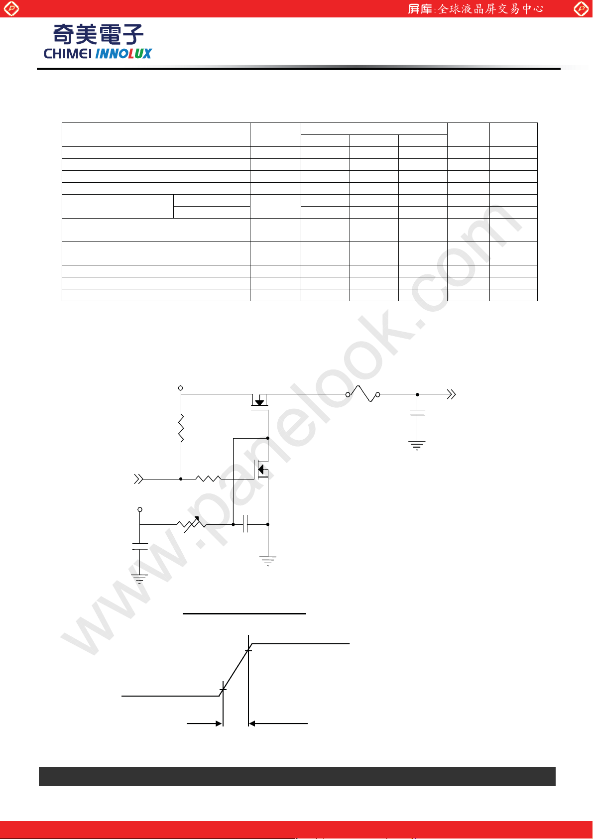
6. INTERFACE TIMING
6.1 TIMING CHARACTERISTICS
The specifications of input signal timing are as the following table and timing diagram.
Signal Item Symbol Min. Typ. Max. Unit Note
DCLK Frequency 1/Tc 50 71 80 MHz -
Vertical Total Time TV 810 823 1023 TH -
DE
Vertical Addressing Time TVD 800 800 800 TH -
Horizontal Total Time TH 1360 1440 1800 Tc -
Horizontal Addressing Time THD 1280 1280 1280 Tc -
www.panelook.com
PRODUCT SPECIFICATION
DE
DCLK
DE
DATA
INPUT SIGNAL TIMING DIAGRAM
T
C
HD
T
Version 2.0 8 February 2012 16 / 27
The copyright belongs to CHIMEI InnoLux. Any unauthorized use is prohibited.
One step solution for LCD / PDP / OLED panel application: Datasheet, inventory and accessory!
www.panelook.com
Page 17

Global LCD Panel Exchange Center
6.2 POWER ON/OFF SEQUENCE
To prevent a latch-up or DC operation of LCD assembly, the power on/off sequence should be as the diagram
below
www.panelook.com
PRODUCT SPECIFICATION
0.9VCC
0.1VCC
VCC
LVDS
0.9Vi
0.1Vi
Vi
PWM DIMMING
BL ON/OFF
T1
T2
VALID
T5
T8
Power ON/OFF sequence
T9
T6
90%
10%
T3
90%
10%
0.9VCC
0.1VCC
T7
T4
0.9Vi
0.1Vi
90%
10%
Note (1) Please avoid floating state of interface signal at invalid period.
Note (2) When the interface signal is invalid, be sure to pull down the power supply of LCD VCC to 0 V.
Note (3) The Backlight converter power must be turned on after the power supply for the logic and the interface
signal is valid. The Backlight converter power must be turned off before the power supply for the logic
and the interface signal is invalid.
Value
Parameter
Units
Min Typ Max
T1 0.5 - 10 ms
T2 0 - 50 ms
T3 0 - 50 ms
T4 500 - - ms
T5 20 - - ms
T6 10 - - ms
T7 5 - 300 ms
T8 10 - - ms
T9 10 - - ms
Version 2.0 8 February 2012 17 / 27
The copyright belongs to CHIMEI InnoLux. Any unauthorized use is prohibited.
One step solution for LCD / PDP / OLED panel application: Datasheet, inventory and accessory!
www.panelook.com
Page 18

Global LCD Panel Exchange Center
7. OPTICAL CHARACTERISTICS
7.1 TEST CONDITIONS
Item Symbol Value Unit
Ambient Temperature Ta
Ambient Humidity Ha
Supply Voltage VCC 3.3 V
Input Signal According to typical value in "3. ELECTRICAL CHARACTERISTICS"
Current I
Converter Duty 100 %
Note (1) If means the forward current of each channel
7.2 OPTICAL SPECIFICATIONS
The relative measurement methods of optical characteristics are shown in 7.2. The following items should
be measured under the test conditions described in 7.1 and stable environment shown in Note (6).
Item Symbol Condition Min. Typ. Max. Unit Note
Red
Green
Color
Chromaticity
Blue
White
Center Luminance of White L
Contrast Ratio CR 550 800 - (2), (6)
Response Time
White Variation
Horizontal
Viewing Angle
Ver t ical
www.panelook.com
PRODUCT SPECIFICATION
o
25±2
50±10
f
Rx
Ry
18±3
0.588
0.357
Gx 0.358
Gy 0.561
Bx 0.158
Typ –
0.05
Typ +
0.05
By 0.150
θ
=0°, θY =0°
Wx 0.313
Wy
C
x
Viewing Normal Angle
0.329
400 500 cd/m2(4), (6)
TR 6 11 Ms
10 15 Ms
T
F
δW
θx+
-
θ
x
θY+
θ
Y
CR 10Њ
-
1.25 1.4 - (5), (6)
60 70
60 70
50 60
50 60
C
%RH
mA
(1), (6)
(3)
Deg. (1), (6)
Version 2.0 8 February 2012 18 / 27
The copyright belongs to CHIMEI InnoLux. Any unauthorized use is prohibited.
One step solution for LCD / PDP / OLED panel application: Datasheet, inventory and accessory!
www.panelook.com
Page 19

Global LCD Panel Exchange Center
T
Note (1) Definition of Viewing Angle (θx, θy):
www.panelook.com
PRODUCT SPECIFICATION
Normal
θx = θy = 0º
θy- θy+
θX- = 90º
6 o’clock
θ
y-
= 90º
x-
y-
Note (2) Definition of Contrast Ratio (CR):
The contrast ratio can be calculated by the following expression.
Contrast Ratio (CR) = L63 / L0
L63: Luminance of gray level 63
L 0: Luminance of gray level 0
CR = CR (5)
CR (X) is corresponding to the Contrast Ratio of the point X at Figure in Note (5).
θx−
θx+
12 o’clock direction
y+
θ
y+
= 90º
x+
θX+ = 90º
Note (3) Definition of Response Time (T
Response
100%
90%
Optical
10%
0%
Gray Level 63
66.68 ms
, TF) and measurement method:
R
T
R
T
F
66.68 ms
Gray Level 63
ime
Version 2.0 8 February 2012 19 / 27
The copyright belongs to CHIMEI InnoLux. Any unauthorized use is prohibited.
One step solution for LCD / PDP / OLED panel application: Datasheet, inventory and accessory!
www.panelook.com
Page 20

Global LCD Panel Exchange Center
Note (4) Definition of Luminance of White (LC):
Measure the luminance of gray level 63 at center point
L
= L (5)
C
L (x) is corresponding to the luminance of the point X at Figure in Note (5).
Note (5) Definition of White Variation (δW):
Measure the luminance of gray level 63 at 5 points
δW = Maximum [L (1), L (2), L (3), L (4), L (5)] / Minimum [L (1), L (2), L (3), L (4), L (5)]
www.panelook.com
PRODUCT SPECIFICATION
Horizontal Line
D
D/4 D/2 3D/4
W/4
W/2
W
Vertical Line
Note (6) Measurement Setup:
The LCD module should be stabilized at given temperature for 20 minutes to avoid abrupt
temperature change during measuring. In order to stabilize the luminance, the measurement
should be executed after lighting Backlight for 20 minutes in a windless room.
3W/4
LCD Module
LCD Panel
1 2
X
: Test Point
X=1 to 5
3
5
4
Active Area
USB2000
CS-2000T
Center of the Screen
500 mm
Light Shield Room
(Ambient Luminance < 2 lux)
Version 2.0 8 February 2012 20 / 27
The copyright belongs to CHIMEI InnoLux. Any unauthorized use is prohibited.
One step solution for LCD / PDP / OLED panel application: Datasheet, inventory and accessory!
www.panelook.com
Page 21

Global LCD Panel Exchange Center
8. RELIABILITY TEST
8.1
RELIABILITY TEST CONDITION
No. Test Item Test Condition Note
1 High Temperature Storage 80 , 240 hoursк
2 Low Temperature Storage -30 , 240 hoursк
3 Thermal Shock Storage {(-30 , 0.5 hour) (к 80 , 0.5 hour)}, 100 cyclesк
4 High Temperature Operating 70 , 240 hoursк
5 Low Temperature Operating -30 , 240 hoursк
6 High Temperature & High Humidity Operating 60 , 90% RH, 240hoursк
7 Shock (Non-Operating) 200G, 2ms, half sine wave, 1 time for ± X, ± Y, ± Z. (3)
www.panelook.com
PRODUCT SPECIFICATION
(1) (2)
8 Vibration (Non-Operating) 1.5G,10~300Hz,10min/cycle,3 cycles each X,Y,Z (3)
Note (1) There should be no condensation on the surface of panel during test.
Note (2) The temperature of panel display surface area should be 80 Max.к
Note (3) At testing Vibration and Shock, the fixture in holding the module has to be hard and rigid enough
so that the module would not be twisted or bent by the fixture.
Note (4) In the standard conditions, there is no function failure issue occurred. All the cosmetic specification
is judged before the reliability test.
Version 2.0 8 February 2012 21 / 27
The copyright belongs to CHIMEI InnoLux. Any unauthorized use is prohibited.
One step solution for LCD / PDP / OLED panel application: Datasheet, inventory and accessory!
www.panelook.com
Page 22

Global LCD Panel Exchange Center
9. PACKAGING
9.1 PACKING SPECIFICATIONS
(1) 20pcs LCD modules / 1 Box
(2) Box dimensions: 520(L)x310(W)x415(H)mm
(3) Weight: approximately 13 Kg (20modules per box)
9.2 PACKING METHOD
(1) Carton Packing should have no failure in the following reliability test items.
Test Item Test Conditions Note
ISTA STANDARD
Random, Frequency Range: 2 – 200 Hz
Vibration
Dropping Test 1 Angle, 3 Edge, 6 Face, 61 cm Non Operation
Top & Bottom: 30 minutes (+Z), 10 min (-Z),
Right & Left: 10 minutes (X)
Back & Forth 10 minutes (Y)
www.panelook.com
PRODUCT SPECIFICATION
Non Operation
Figure. 9-1 Packing method
Version 2.0 8 February 2012 22 / 27
The copyright belongs to CHIMEI InnoLux. Any unauthorized use is prohibited.
One step solution for LCD / PDP / OLED panel application: Datasheet, inventory and accessory!
www.panelook.com
Page 23

Global LCD Panel Exchange Center
www.panelook.com
PRODUCT SPECIFICATION
Figure. 9-2 Packing method
Version 2.0 8 February 2012 23 / 27
The copyright belongs to CHIMEI InnoLux. Any unauthorized use is prohibited.
One step solution for LCD / PDP / OLED panel application: Datasheet, inventory and accessory!
www.panelook.com
Page 24

Global LCD Panel Exchange Center
www.panelook.com
PRODUCT SPECIFICATION
10. DEFINITION OF LABEL
10.1 CMI MODULE LABEL
The barcode nameplate is pasted on each module as illustration, and its definitions are as following explanation.
CHI MEI
OPTOELECTRONICS
(a) Model Name: G133IGE -L03
(b) Revision: Rev. XX, for example: A1, …, C1, C2 …etc.
(c) Serial ID: X X
Serial ID includes the information as below:
X X X X X Y M D X N N N N
G133IGE -L03 Rev.XX
X X X X X X X Y M D L N N N N
Serial No.
CMI Internal Use
Year, Month, Date
CMI Internal Use
Revision
CMI Internal Use
E207943
MADE IN TAIWAN
RoHS
(a) Manufactured Date: Year: 1~9, for 2011~2019
Month: 1~9, A~C, for Jan. ~ Dec.
Day: 1~9, A~Y, for 1
(b) Revision Code: cover all the change
Serial No.: Manufacturing sequence of product
st
to 31st, exclude I , O and U
Version 2.0 8 February 2012 24 / 27
The copyright belongs to CHIMEI InnoLux. Any unauthorized use is prohibited.
One step solution for LCD / PDP / OLED panel application: Datasheet, inventory and accessory!
www.panelook.com
Page 25

Global LCD Panel Exchange Center
www.panelook.com
PRODUCT SPECIFICATION
11. PRECAUTIONS
11.1 ASSEMBLY AND HANDLING PRECAUTIONS
(1) Do not apply rough force such as bending or twisting to the module during assembly.
(2) To assemble or install module into user’s system can be only in clean working areas. The dust and oil
may cause electrical short or worsen the polarizer.
(3) It’s not permitted to have pressure or impulse on the module because the LCD panel and Backlight will
be damaged.
(4) Always follow the correct power sequence when LCD module is connecting and operating. This can
prevent damage to the CMOS LSI chips during latch-up.
(5) Do not pull the I/F connector in or out while the module is operating.
(6) Do not disassemble the module.
(7) Use a soft dry cloth without chemicals for cleaning, because the surface of polarizer is very soft and
easily scratched.
(8) It is dangerous that moisture come into or contacted the LCD module, because moisture may damage
LCD module when it is operating.
(9) High temperature or humidity may reduce the performance of module. Please store LCD module within
the specified storage conditions.
(10) When ambient temperature is lower than 10ºC may reduce the display quality. For example, the
response time will become slowly.
(11) Do not keep same pattern in a long period of time. It may cause image sticking on LCD
11.2 SAFETY PRECAUTIONS
(1) Do not disassemble the module or insert anything into the Backlight unit to prevent electrical shock.
(2) If the liquid crystal material leaks from the panel, it should be kept away from the eyes or mouth. In
case of contact with hands, skin or clothes, it has to be washed away thoroughly with soap.
(3) After the module’s end of life, it is not harmful in case of normal operation and storage.
Version 2.0 8 February 2012 25 / 27
The copyright belongs to CHIMEI InnoLux. Any unauthorized use is prohibited.
One step solution for LCD / PDP / OLED panel application: Datasheet, inventory and accessory!
www.panelook.com
Page 26

Global LCD Panel Exchange Center
www.panelook.com
One step solution for LCD / PDP / OLED panel application: Datasheet, inventory and accessory!
www.panelook.com
Page 27

Global LCD Panel Exchange Center
www.panelook.com
One step solution for LCD / PDP / OLED panel application: Datasheet, inventory and accessory!
www.panelook.com
 Loading...