

Page 1
Chimei-Innolux Corporation
BT140GW02 V.9 LCD MODULE SPECIFICATION
( ) Preliminary Specification
(●) Final Specification
Customer Checked & Approved by
ASUS
Approved by Checked by Prepared by
MKT PD PM
楊竣傑 柯瑞峰 詹銘斯 陳郁甫
Chimei-Innolux Corporation
No.160 Kesyue Rd., Chu-Nan Site, Hsinchu Science Park,
Date: 2011/05/06
Chu-Nan 350, Miao-Li County, Taiwan
Tel: 886-37-586000 Fax: 886-37-586060
Page 2

Version: 4
Record of Revision
Version Revise Date Page Content
Ch i me i- I nn o lu x copyright
All rights reserved,
Copying forbidden.
0 2010/05/13
1 2010/05/19
2 2010/10/08
3 2010/10/19
4 2011/05/06
All First Edition issued
22 Label
16 OPT Spec
21,22 Label drawing
23 Package Drawing
25,26 Label position
27 EDID code
5,6 Modify LVDS connector source
21,22,26 Label Logo
Page 3

SPEC NO.
PAGE
BT140GW02 V.9
3/30
Contents: Page
1 . General Specifications
2 . Electrical Specifications
2-1 Pin Assignment
2-2 Absolute Maximum Ratings
2-3 Electrical Characteristics
3 . Optical Specifications
4. Reliability Test Items
5. Safety
6. Display Quality
7. Handling Precaution
8. Label Definition
2
3
5
6
14
17
18
18
18
19
9. Packing Form
10. Mechanical Drawings
11. System Cover Design Notice
Appendix
21
22
24
25
ALL RIGHTS STRICTLY RESERVED. ANY PORTION OF THIS DOCUMENT SHALL NOT BE REPRODUCED, COPIED, OR
TRANSFORMED TO ANY OTHE R F OR MS WITHOUT PERMISSION FR OM Chimei-Innolux
Page 4
SPEC NO.
PAGE
BT140GW02 V.9
4/30
1. General Specifications
NO. Item Specification Unit
1 Display resolution (pixel) 1366(H) X 768(V), HD resolution
2 Active area 309.40(H) X 173.95(V) mm
3 Screen size 14.0 inches diagonal Inches
4 Pixel pitch 0.2265(H) X 0.2265(V) mm
5 Color configuration Stripe
6 Overall dimension
7 Weight
324(W) X 192.5(H) X 5.2(D) (max)
350Max.
mm
Grams
8 Surface treatment Anti Glare
9 Input color signal 6 bit LVDS
10 Display colors 262K (6 bit)
11 Optimum viewing direction 6 o’clock
12 Backlight W-LED
13 Glass thickness 0.5 mm
14 LED life time with LCM 12,000 (min.), T = 25°C Hours
15 RoHS RoHS compliance
ALL RIGHTS STRICTLY RESERVED. ANY PORTION OF THIS DOCUMENT SHALL NOT BE REPRODUCED, COPIED, OR
TRANSFORMED TO ANY OTHE R F OR MS WITHOUT PERMISSION FR OM Chimei-Innolux
Page 5

SPEC NO.
PAGE
BT140GW02 V.9
5/30
2. Electrical Specifications
2-1 Pin Assignment
a. Panel connector
Connector Part No:
User’s connector Part No: 20453-040T-12(I-PEX) or equivalent
Pin No Symbol Description Remark
1 NC No connection (Reserve)
2 VCC Power Supply (+3.3V)
3 VCC Power Supply (+3.3V)
4 V
5
6 Clk
7 DATA
8 Rxin0- Differential Data Input
9 Rxin0+ Differential Data Input
10 GND Ground
11 Rxin1- Differential Data Input
12 Rxin1+ Differential Data Input
13 GND Ground
14 Rxin2- Differential Data Input
15 Rxin2+ Differential Data Input
16 GND Ground
17 CLK- Differential Clock Input
18 CLK+ Differential Clock Input
19 GND Ground
20 NC No connection (Reserve)
21 NC No connection (Reserve)
22 GND Ground
23 NC No connection (Reserve)
24 NC No connection (Reserve)
25 GND Ground
26 NC No connection (Reserve)
27 NC No connection (Reserve)
28 GND Ground
29 NC No connection (Reserve)
30 NC No connection (Reserve)
31 LED_GND LED Ground
32 LED_GND LED Ground
33 LED_GND LED Ground
34
35 LED_PWM PWM dimming signal input
36 LED_EN LED enable pin (3.3V)
37 NC No connection (Reserve)
38 V_LED LED power supply 6V~21V
39 V_LED LED power supply 6V~21V
40 V_LED LED power supply 6V~21V
GS13401-1110S (Foxconn ) & 20455-040E-12 (I-PEX)
DDC Power +3.3V
EDID
NC No connection (Reserve)
DDC Clock
EDID
DDC Data
EDID
R0~R5,G0
G1~G5,B0,B1
B2~B5,DE,Hsync,Vsync
NC No connection (Reserve)
ALL RIGHTS STRICTLY RESERVED. ANY PORTION OF THIS DOCUMENT SHALL NOT BE REPRODUCED, COPIED, OR
TRANSFORMED TO ANY OTHE R F OR MS WITHOUT PERMISSION FR OM Chimei-Innolux
Page 6
(Ip
)
SPEC NO.
PAGE
BT140GW02 V.9
6/30
b. General block diagram (Rear-side)
FPC
FPC
LED
Drive
DC/DC
VR
GS13401-1110S or 20455-040E-12
T-CON
Connector plug in direction
Pin1
GS13401-1110S (Foxconn ) or
20455-040E-12
ex
ALL RIGHTS STRICTLY RESERVED. ANY PORTION OF THIS DOCUMENT SHALL NOT BE REPRODUCED, COPIED, OR
TRANSFORMED TO ANY OTHE R F OR MS WITHOUT PERMISSION FR OM Chimei-Innolux
Page 7
V
SPEC NO.
PAGE
BT140GW02 V.9
7/30
2-2. Absolute Maximum Ratings
Parameter Symbol
alues
Unit
Remark
Min. Max.
Power input voltage V
Signal input voltage V
LED input voltage V
Operating temperature T
Storage temperature T
- 0.3 4.0 V At 25℃
CC
- 0.3 4.0 V At 25℃
IN
- 0.3 30 V At 25℃
LED
0 50 ℃ Note 1
OP
- 20 60 ℃ Note 2
ST
Re-screw - 5 Times
Assured torque at side mount - 2 kgf.cm
Note 1: The relative humidity must not exceed 90%, non-condensing at temperatures of 40℃ or
less. At temperatures greater than 40℃, the wet bulb temperature must not exceed 39℃.
Note 2: The unit should not be exposed to corrosive chemicals.
Relative Humidity (%RH)
100
90
80
70
60
50
Operation Range
-30 -20 -10 0 10 20 30 40 50 60 70
40
30
20
Storage Range
10
0
Temperature (°C)
ALL RIGHTS STRICTLY RESERVED. ANY PORTION OF THIS DOCUMENT SHALL NOT BE REPRODUCED, COPIED, OR
TRANSFORMED TO ANY OTHE R F OR MS WITHOUT PERMISSION FR OM Chimei-Innolux
Page 8
SPEC NO.
PAGE
BT140GW02 V.9
8/30
2-3. Electrical Characteristics
a. Typical operating conditions
Item Symbol Min. Typ. Max. Unit Remark
Power input voltage
Permissive power input ripple
Power input current
Power consumption
Differential input high
threshold voltage
Differential input low
LVDS
interface
threshold voltage
Common input
voltage
Terminating resistor
Rush current
LED rush current
V
3 3.3 3.6 V
CC
V
- - 0.1 V
RF
I
- 300 330 mA Note 1
CC
P
- 1 Watts Note 1
C
V
- - +100 mV
LVT H
V
-100 - - mV
LVT L
V
1.0 1.2 1.4 V
LVC
R
90 100 110 ohm
T
I
- - 1.5 A Note 3
Rush
I
LED-Rush
- - 3.0 A Note 4
Note 1: The specified input current and power consumption are under the V
f
=60Hz (frame frequency) condition whereas mosaic pattern is displayed.
V
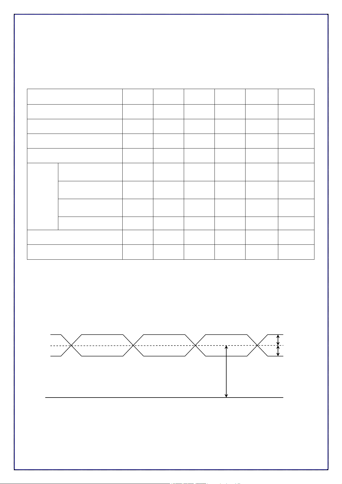
Note 2: LVDS waveform diagram
Rxin+/CLK+
Rxin-/CLK-
interface
=3.3 V, 25°C,
cc
LVDS
V
LVT H
V
LVT L
V
LVC
GND
ALL RIGHTS STRICTLY RESERVED. ANY PORTION OF THIS DOCUMENT SHALL NOT BE REPRODUCED, COPIED, OR
TRANSFORMED TO ANY OTHE R F OR MS WITHOUT PERMISSION FR OM Chimei-Innolux
Page 9
SPEC NO.
PAGE
BT140GW02 V.9
9/30
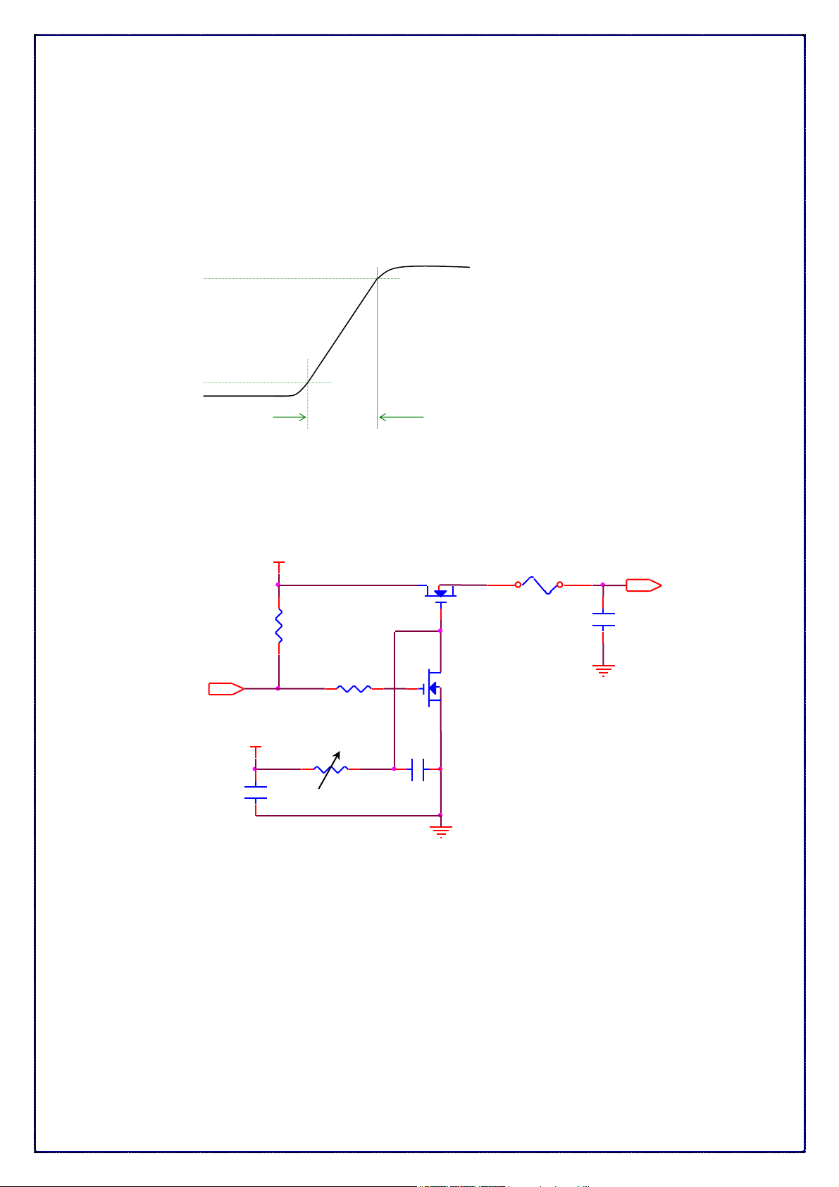
Note 3: Test condition
(1) Pattern: Black pattern
(2) V
= 3.3 V, V
CC
rising time = 470 μs ± 10%
CC
Control signal
(High to low)
90%
10%
(3) Test circuit
12V
V
CC
Ton=470µs±10%
3.3 V
C3
1uF
R1
47K
R2
1K
R3
47K
M1
2SK1059
C2
10000pF
M2
2SK1399
FUSE
VCC ( LCD input)
C1
1uF
ALL RIGHTS STRICTLY RESERVED. ANY PORTION OF THIS DOCUMENT SHALL NOT BE REPRODUCED, COPIED, OR
TRANSFORMED TO ANY OTHE R F OR MS WITHOUT PERMISSION FR OM Chimei-Innolux
Page 10

_
SPEC NO.
PAGE
BT140GW02 V.9
10/30
Note 4: Test condition
(1) Pattern: LED duty 100%
(2) V_LED = 12.0V, V_LED rising time = 470
μs ± 10%
Control signal
(High to low)
90%
10%
(3) Test circuit
21V
V
LED
Ton=470µs±10%
12 V
C3
1uF
R1
47K
R2
1K
R3
47K
M1
2SK1059
C2
10000pF
M2
2SK1399
FUSE
V_LED
C1
1uF
ALL RIGHTS STRICTLY RESERVED. ANY PORTION OF THIS DOCUMENT SHALL NOT BE REPRODUCED, COPIED, OR
TRANSFORMED TO ANY OTHE R F OR MS WITHOUT PERMISSION FR OM Chimei-Innolux
Page 11

SPEC NO.
PAGE
BT140GW02 V.9
11/30
b. Power sequence
Power supply for LCD, VCC
Interface data signal, V
(LVDS signal of transmitter)
i
Backlight on/off
Power sequence timing table
Parameter
Min. Typ. Max.
90%
10%
0V
T1
T
2
0V
OFF OFF
Valid Data
T
3
T
Backlight
On
Value
90%
10%
T
T
T
5
4
7
6
Units
T1 0.5 - 10 ms
T2 0 - 50 ms
T3 200 - - ms
T4 200 - - ms
T5 0 - 50 ms
T6 0.5 - 10 ms
T7 400 - - ms
ALL RIGHTS STRICTLY RESERVED. ANY PORTION OF THIS DOCUMENT SHALL NOT BE REPRODUCED, COPIED, OR
TRANSFORMED TO ANY OTHE R F OR MS WITHOUT PERMISSION FR OM Chimei-Innolux
Page 12

c. Display color vs. input data signals
Signal Name Description Remark
SPEC NO.
PAGE
BT140GW02 V.9
12/30
R5 Red Data 5 (MSB)
R4 Red Data 4
R3 Red Data 3
R2 Red Data 2
R1 Red Data 1
R0 Red Data 0 (LSB)
Red-pixel Data
G5 Green Data 5 (MSB)
G4 Green Data 4
G3 Green Data 3
G2 Green Data 2
G1 Green Data 1
G0 Green Data 0 (LSB)
Green-pixel Data
B5 Blue Data 5 (MSB)
B4 Blue Data 4
B3 Blue Data 3
B2 Blue Data 2
Red-pixel data. Each red pixel's brightness data
consists of these 6 bits pixel data.
Green-pixel data. Each green pixel's brightness
data consists of these 6 bits pixel data.
Blue-pixel data. Each blue pixel's brightness data
consists of these 6 bits pixel data.
B1 Blue Data 1
B0 Blue Data 0 (LSB)
Blue-pixel Data
Signal for 1 DCLK cycle (t
)
CLK
ALL RIGHTS STRICTLY RESERVED. ANY PORTION OF THIS DOCUMENT SHALL NOT BE REPRODUCED, COPIED, OR
TRANSFORMED TO ANY OTHE R F OR MS WITHOUT PERMISSION FR OM Chimei-Innolux
Page 13

SPEC NO.
PAGE
BT140GW02 V.9
13/30
d. Input signal timing
Timing table
Description Symbol Min Typ Max Unit
Frame rate -- 40 60 -- Hz
Clock freq. 1/t
45 71 85 MHz
CLK
Line cycle time tH 1400 1498 1800
Line width-active tHd 1366 1366 1366
Frame cycle time tV 780 790 900 tH
V width-active tVd 768 768 768 tH
t
Vd
t
V
DE
t
t
DE
t
CLK
Hd
H
t
CLK
t
CLK
DCLK
e. Display position
D(1, 1) D(2, 1) …… D(683, 1) …… D(1365, 1) D(1366, 1)
D(1, 2) D(2, 2) …… D(683, 2) …… D(1365, 2) D(1366, 2)
.
.
.
……
.
.
.
……
.
.
.
.
.
.
D(1, 384) D(2, 384) …… D(683, 384) …… D(1365, 384) D(1366, 384)
.
.
.
……
.
.
.
……
.
.
.
.
.
.
D(1, 767) D(2, 767) …… D(683, 767) …… D(1365, 767) D(1366, 767)
D(1, 768) D(2, 768) …… D(683, 768) …… D(1365, 768) D(1366, 768)
ALL RIGHTS STRICTLY RESERVED. ANY PORTION OF THIS DOCUMENT SHALL NOT BE REPRODUCED, COPIED, OR
TRANSFORMED TO ANY OTHE R F OR MS WITHOUT PERMISSION FR OM Chimei-Innolux
Page 14

f. Backlight driving conditions
Parameter Symbol Min. Typ. Max. Unit Remark
SPEC NO.
PAGE
BT140GW02 V.9
14/30
Gate driver
T = 25°C
T = 25°C
T = 25°C
Note 1
=3.3 V, 25 °
cc
LED forward voltage V
LED forward current
LED power consumption
Input PWM frequency F
Duty ratio - 5 100 % Note 2
LED life time (LED only) - 15,000 Hr T = 25°C , Note 3
Note 1: The BL power consumption @100 nits with full white pattern under the V
C, f
=60Hz (frame frequency) condition
V
Note 2: PWM duty ratio linearity guarantees 10~100%.
Note 3: LED life time definition is brightness decrease to 50% of initial or abnormal lighting.
g. Module function block
LED driver
Timing
controller
3 3.2 3.4 V
F
IF 20 mA
P
2.8 3 W
LED
P
1.2 W
LED-G
190 1000 2000 Hz T = 25°C
PWM
rms
rms
LED Light-bar
TFT-LCD
Source driver
Step-up regulator
& reference voltage
generator
EDID
EEPROM
LVDS connector
LVDS DATA BUS mini-LVDS & CONTROL BUS POWER I2C BUS
ALL RIGHTS STRICTLY RESERVED. ANY PORTION OF THIS DOCUMENT SHALL NOT BE REPRODUCED, COPIED, OR
TRANSFORMED TO ANY OTHE R F OR MS WITHOUT PERMISSION FR OM Chimei-Innolux
Page 15

h. LED circuit block
SPEC NO.
PAGE
BT140GW02 V.9
15/30
LED Driving
Circuit
4 parallels
& 9 series
FB1
FB2
LED_P
FB3
FB4
ALL RIGHTS STRICTLY RESERVED. ANY PORTION OF THIS DOCUMENT SHALL NOT BE REPRODUCED, COPIED, OR
TRANSFORMED TO ANY OTHE R F OR MS WITHOUT PERMISSION FR OM Chimei-Innolux
Page 16

SPEC NO.
PAGE
BT140GW02 V.9
16/30
3. Optical specifications
Ambient temperature = 25℃
Item Symbol Condition
Specification
Min. Typ. Max.
Unit Remark
Response time
Contrast ratio CR
Viewing angle
Brightness
(5 points average)
Tr+Tf θ= 0°
θ= 0°
500 Note 2,4
8 15 ms Note 3
Top 15
Bottom 30
CR≧10
Left 40
Right
40
deg Note 2,4,6
Top 6
Bottom 11
CR≧100
Left 25
Right
Y
187 220 nit Note 2,5
L
Wx
Wy
25
0.313
0.329
Color chromaticity (CIE)
Rx
Ry
Gx
Gy
Bx
B
θ= 0°
y
-0.03
0.586
0.355
0.323
0.57
0.163
0.141
+0.03
Note 2
Color gamut NTSC CIE1931 45 % -
δ
1.25
W(5)
White uniformity
1.5
δ
W(13)
Note 2,7
Cross talk Ct 2% Note 8
ALL RIGHTS STRICTLY RESERVED. ANY PORTION OF THIS DOCUMENT SHALL NOT BE REPRODUCED, COPIED, OR
TRANSFORMED TO ANY OTHE R F OR MS WITHOUT PERMISSION FR OM Chimei-Innolux
Page 17

(
Avg
)
SPEC NO.
PAGE
BT140GW02 V.9
17/30
Note 1: To be measured in dark room.
Note 2: To be measured with a viewing cone of 2°by Topcon luminance meter BM-5A.
Note 3: Definition of response time:
The output signals of BM-7 are measured when the input pattern are changed from “Black” to
“White” (falling time) and from “White” to “Black” (rising time), respectively. The response time
interval is between 10% and 90% of amplitudes. Refer to figure as below.
100%
S
i
90%
g
n
a
l
(
R
e
l
a
t
i
v
e
v
a
l
u
10%
e
)
0%
Tr
Note 4: Definition of contrast ratio:
Contrast ratio is calculated with the following formula:
Contrast ratio
of 5pts
=
Note 5: Driving current for LED should be 20 mA.
Luminance is measured at the following thirteen points (1~13):
Y
= (Y5+ Y10+Y11+Y12 +Y13) / 5
L
Note 6: Definition of viewing angle
"Black"
L white (Avg of 5pts.)
L
Black (Avg of 5pts.)
"White""White"
Tf
ALL RIGHTS STRICTLY RESERVED. ANY PORTION OF THIS DOCUMENT SHALL NOT BE REPRODUCED, COPIED, OR
TRANSFORMED TO ANY OTHE R F OR MS WITHOUT PERMISSION FR OM Chimei-Innolux
Page 18

SPEC NO.
PAGE
BT140GW02 V.9
18/30
Note 7: Definition white uniformity
Luminance is measured at the following thirteen points (1~13):
δ
Maximum brightness of thirteen points
W(13) =
δ
W(5) =
Minimum brightness of thirteen points
Maximum brightness of five points
Minimum brightness of five points
13 point measuring locations refer to the point 1, 2, 3, 4, 5, 6, 7, 8, 9, 10, 11, 12 and 13.
5 point measuring locations refer to the point 5, 10, 11, 12 and 13.
Note 8:
1/2
1/6
A
B
32 gray level 32 gray level
Unit: percentage of dimension of display area
l L
l L
l / LA x 100%= 2% max., LA and L
A-LA’
l / LB x 100%= 2% max., LB’ and LB’ are brightness at location B and B’
B-LB’
1/6
1/2
2/3 1/3
1/2
A’
0 gray level
are brightness at location A and A’
A’
1/6
1/6
1/3
1/2
B’
2/3
ALL RIGHTS STRICTLY RESERVED. ANY PORTION OF THIS DOCUMENT SHALL NOT BE REPRODUCED, COPIED, OR
TRANSFORMED TO ANY OTHE R F OR MS WITHOUT PERMISSION FR OM Chimei-Innolux
Page 19

SPEC NO.
PAGE
BT140GW02 V.9
19/30
4. Reliability test items
Test Item Test Condition Judgment Remark
High temperature storage
Low temperature storage
High temperature & high
humidity operation
High temperature operation
Low temperature operation
Thermal shock
(Non-operation)
Electrostatic discharge (ESD)
Vibration
(Non-operation)
Mechanical shock
(Non-operation)
60℃, 240 hours
-20℃, 240 hours
40°C, 90% RH, 240 hours
(No condensation)
50℃, 240 hours
0℃, 240 hours
-25°C / 30 mins ~ -65°C / 30 mins
100 cycles
150 pF, 330Ω,
Contact: ±8kV, Air: ±15kV
1.5G, 10 to 500 Hz random; 0.5hr in each
perpendicular axes ( X, Y, Z ).
220G/2ms, Half sine wave, ±X, ±Y, ±Z one
time for each direction
Note 1 Note 2
Note 1 Note 2
Note 1 Note 2
Note 1 Note 2
Note 1 Note 2
Note 1 Note 2
Note 1
Note 1 Note 2
Note 1 Note 2
Note 1: Pass: Normal display image with no obvious non-uniformity and no line defect.
Fail: No display image, obvious non-uniformity, or line defects.
Partial transformation of the module parts should be ignored.
Note 2: Evaluation should be tested after storage at room temperature more than one hour.
ALL RIGHTS STRICTLY RESERVED. ANY PORTION OF THIS DOCUMENT SHALL NOT BE REPRODUCED, COPIED, OR
TRANSFORMED TO ANY OTHE R F OR MS WITHOUT PERMISSION FR OM Chimei-Innolux
Page 20

SPEC NO.
PAGE
BT140GW02 V.9
20/30
5. Safety
5-1. Sharp edge requirements
There will be no sharp edges or corners on the display assembly that could cause injury.
5-2. Materials
a. Toxicity
There will be no carcinogenic materials used anywhere in the display module. If toxic materials
are used, they will be reviewed and approved by the responsible InnoLux Toxicologist.
b. Flammability
All components including electrical components that do not meet the flammability grade UL94-V0
in the module will complete the flammability rating exception approval process. The printed circuit
board will be made from material rated 94-V0 or better. The actual UL flammability rating will be
printed on the printed circuit board.
c. Capacitors
If any polarized capacitors are used in the display assembly, provisions will be made to keep
them from being inserted backwards.
6. Display quality
The display quality of the color TFT-LCD module should be in compliance with the InnoLux
incoming inspection standard.
7. Handling precaution
(1) Do not apply rough force such as bending or twisting to the module during assembly.
(2) To assemble or install module into user’s system can be only in clean working areas. The
dust and oil may cause electrical short or worsen the polarizer.
(3) It’s not permitted to have pressure or impulse on the module because the LCD panel and
backlight will be damaged.
(4) Always follow the correct power sequence when LCD module is connecting and
operating.
(5) Do not pull the I/F connector in or out while the module is operating.
(6) Do not disassemble the module.
(7) Use a soft dry cloth without chemicals for cleaning, because the surface of polarizer is
very soft and easily scratched.
(8) It is dangerous that moisture come into or contacted the LCD module, because moisture
may damage LCD module when it is operating.
(9) High temperature or humidity may reduce the performance of module. Please store LCD
module within the specified storage conditions.
ALL RIGHTS STRICTLY RESERVED. ANY PORTION OF THIS DOCUMENT SHALL NOT BE REPRODUCED, COPIED, OR
TRANSFORMED TO ANY OTHE R F OR MS WITHOUT PERMISSION FR OM Chimei-Innolux
Page 21

SPEC NO.
PAGE
BT140GW02 V.9
21/30
8. Label Definition
8-1. Module label
(a) Model Number : BT140GW02 V.9
(b) Product Number : AB140000290X
(c) Serial ID: X X X X X X X Y M D L N N N N
(d) Production Location: MADE IN XXXX.
(e) UL/CB logo: “XXXX” especially stands for panel manufactured by CMI Ningbo satisfying UL/CB requirement.
“LEOO” “CANO” is the CMI’s UL factory code for Ningbo factory.
Serial No.
Product stroke
Year, Month, Date
CMI Internal Use
Revision
CMI Internal Use
Serial ID II (INL Internal Use):
Z1 Z2 –Z3 Z4 Z5 Z6 Z7 –Z8– Z9 –Z10 –Z11 Z12– Z13–Z14 Z15– Z16– Z17 Z18 Z19–Z20 Z21 Z22 Z
23
ALL RIGHTS STRICTLY RESERVED. ANY PORTION OF THIS DOCUMENT SHALL NOT BE REPRODUCED, COPIED, OR
TRANSFORMED TO ANY OTHE R F OR MS WITHOUT PERMISSION FR OM Chimei-Innolux
Page 22

SPEC NO.
PAGE
BT140GW02 V.9
22/30
8-2. Carton label
(a) Model No. : BT140GW02 V.9
(b) Package Quantity: XXPCS
(c) Serial ID: X X X X X X X Y M D L N N N
Serial No.
Product stroke
Year, Month, Date
CMI Internal Use
Revision
CMI Internal Use
ALL RIGHTS STRICTLY RESERVED. ANY PORTION OF THIS DOCUMENT SHALL NOT BE REPRODUCED, COPIED, OR
TRANSFORMED TO ANY OTHE R F OR MS WITHOUT PERMISSION FR OM Chimei-Innolux
Page 23

p
r
SPEC NO.
PAGE
BT140GW02 V.9
23/30
9. Packing Form
Lowe
Carton
25 pcs
Cushion
Step E
Ste
F
Upper Cushion
ALL RIGHTS STRICTLY RESERVED. ANY PORTION OF THIS DOCUMENT SHALL NOT BE REPRODUCED, COPIED, OR
TRANSFORMED TO ANY OTHE R F OR MS WITHOUT PERMISSION FR OM Chimei-Innolux
Page 24

SPEC NO.
PAGE
BT140GW02 V.9
24/30
10. Mechanical Drawings
10-1. Front side
ALL RIGHTS STRICTLY RESERVED. ANY PORTION OF THIS DOCUMENT SHALL NOT BE REPRODUCED, COPIED, OR
TRANSFORMED TO ANY OTHE R F OR MS WITHOUT PERMISSION FR OM Chimei-Innolux
Page 25

SPEC NO.
PAGE
BT140GW02 V.9
25/30
10-2 Rear side
BT140GW01 8YBXXXXX-
INL SN: Z1Z2Z3Z4-Z5-Z6-Z7Z 8Z9-Z10Z11-Z12Z13Z14Z15-Z 16-Z1-7Z18Z19
ALL RIGHTS STRICTLY RESERVED. ANY PORTION OF THIS DOCUMENT SHALL NOT BE REPRODUCED, COPIED, OR
TRANSFORMED TO ANY OTHE R F OR MS WITHOUT PERMISSION FR OM Chimei-Innolux
Page 26

SPEC NO.
PAGE
BT140GW02 V.9
26/30
ALL RIGHTS STRICTLY RESERVED. ANY PORTION OF THIS DOCUMENT SHALL NOT BE REPRODUCED, COPIED, OR
TRANSFORMED TO ANY OTHE R F OR MS WITHOUT PERMISSION FR OM Chimei-Innolux
Page 27

SPEC NO.
PAGE
BT140GW02 V.9
27/30
Appendix: EDID Code
Byte
(Hex)
Header
00
Header
01
Header
02
Header
03
Header
04
Header
EDID Version
Vendor / Product
Display
Parameters
Panel Color Coordinates
Header
05
Header
06
Header
07
EISA manufacture code ( 3 Character ID ) " CMO"
08
EISA manufacture code (Compressed ASCⅡ)
09
Panel Supplier Reserved - Product Code "44"
0A
( Hex. LSB first )
0B
LCD Module Serial No - Preferred but Optional ("0" If not used)
0C
LCD Module Serial No - Preferred but Optional ("0" If not used)
0D
LCD Module Serial No - Preferred but Optional ("0" If not used)
0E
LCD Module Serial No - Preferred but Optional ("0" If not used)
0F
Week of Manufacture
10
00 weeks
Year of Manufacture
11
2010 years
EDID structure version # = 1
12
EDID revision # = 3
13
Video input Definition = Digital signal
14
Max H image size (Rounded cm) = 31 cm
15
Max V image size (Rounded cm) = 18 cm
16
Display gamma = (gamma*100)-100 = Example:(2.2*100)-100=120 = 2.2 Gamma
17
Feature Support (no_DPMS, no_Active Off/Ve ry Low Power, RGB color display, Timing
18
BLK 1,no_ GTF)
Red/Green Low Bits (RxRy/GxGy)
19
Blue/White Low Bits (BxBy/WxWy)
1A
Red X Rx = 0.586
1B
Red Y Ry = 0.355
1C
Green X Gx = 0.323
1D
Green Y Gy = 0.550
1E
Blue X Bx = 0.155
1F
Blue Y By = 0.155
20
White X Wx = 0.313
21
White Y Wy = 0.329
22
Field Name and Comments
Value
(Hex)
00
FF
FF
FF
FF
FF
FF
00
0D
AF
2C
00
00
00
00
00
00
14
01
03
80
1F
12
78
0A
0C
C5
96
5B
52
92
29
24
50
54
Value
(Bin)
00000000
11111111
11111111
11111111
11111111
11111111
11111111
00000000
00001101
10101111
00101100
00000000
00000000
00000000
00000000
00000000
00000000
00010100
00000001
00000011
10000000
00011111
00010010
01111000
00001010
00001100
11000101
10010110
01011011
01010010
10010010
00101001
00100100
01010000
01010100
ALL RIGHTS STRICTLY RESERVED. ANY PORTION OF THIS DOCUMENT SHALL NOT BE REPRODUCED, COPIED, OR
TRANSFORMED TO ANY OTHE R F OR MS WITHOUT PERMISSION FR OM Chimei-Innolux
Page 28

SPEC NO.
PAGE
BT140GW02 V.9
28/30
Established timing 1 (00h if not used)
23
Established timing 2 (00h if not used)
24
Timings
Established
Standard Timing ID
Timing Descriptor #1
Manufacturer's timings (00h if not used)
25
Standard timing ID1 (01h if not used)
26
Standard timing ID1 (01h if not used)
27
Standard timing ID2 (01h if not used)
28
Standard timing ID2 (01h if not used)
29
Standard timing ID3 (01h if not used)
2A
Standard timing ID3 (01h if not used)
2B
Standard timing ID4 (01h if not used)
2C
Standard timing ID4 (01h if not used)
2D
Standard timing ID5 (01h if not used)
2E
Standard timing ID5 (01h if not used)
2F
Standard timing ID6 (01h if not used)
30
Standard timing ID6 (01h if not used)
31
Standard timing ID7 (01h if not used)
32
Standard timing ID7 (01h if not used)
33
Standard timing ID8 (01h if not used)
34
Standard timing ID8 (01h if not used)
35
Pixel Clock/10,000 (LSB)
36
71 MHz @ 60Hz
Pixel Clock/10,000 (MSB)
37
Horizontal Active (lower 8 bits) 1366 Pixels
38
Horizontal Blanking(Thp-HA) (lower 8 bits) 132 Pixels
39
Horizontal Active / Horizontal Blanking(Thp-HA) (upper 4:4bits)
3A
Vertical Avtive 768 Lines
3B
Vertical Blanking (Tvp-HA) (DE Blanking typ.for DE only panels) 22 Lines
3C
Vertical Active : Vertical Blanking (Tvp-HA) (upper 4:4bits)
3D
Horizontal Sync. Offset (Thfp) 48 Pixels
3E
Horizontal Sync Pulse Width (HSPW) 32 Pixels
3F
Vertical Sync Offset(Tvfp) : Sync Width (VSPW) 1 Lines : 4 Lines
40
Horizontal Vertical Sync Offset/Width (upper 2bits)
41
Horizontal Image Size (mm) 309 mm
42
Vertical Image Size (mm) 174 mm
43
Horizontal Image Size / Vertical Image Size
44
Horizontal Border = 0 (Zero for Notebook LCD)
45
Vertical Border = 0 (Zero for Notebook LCD)
46
Non-Interlace, Normal display, no stereo, Digital Separate ( Vsync_NEG, Hsync_NEG ), DE
47
only note : LSB is set to '1' if panel is DE-timing only. H/V can be ignored.
00
00
00
01
01
01
01
01
01
01
01
01
01
01
01
01
01
01
01
BC
1B
56
84
50
00
16
30
30
20
14
00
35
AE
10
00
00
18
00000000
00000000
00000000
00000001
00000001
00000001
00000001
00000001
00000001
00000001
00000001
00000001
00000001
00000001
00000001
00000001
00000001
00000001
00000001
10111100
00011011
01010110
10000100
01010000
00000000
00010110
00110000
00110000
00100000
00010100
00000000
00110101
10101110
00010000
00000000
00000000
00011000
ALL RIGHTS STRICTLY RESERVED. ANY PORTION OF THIS DOCUMENT SHALL NOT BE REPRODUCED, COPIED, OR
TRANSFORMED TO ANY OTHE R F OR MS WITHOUT PERMISSION FR OM Chimei-Innolux
Page 29

SPEC NO.
PAGE
BT140GW02 V.9
29/30
Flag
48
Flag
49
Flag
4A
Data Type Tag (Descriptor Defined by manufacturer )
4B
Flag
4C
Descriptor Defined by manufacturer
4D
Descriptor Defined by manufacturer
4E
Descriptor Defined by manufacturer
4F
Descriptor Defined by manufacturer
50
Descriptor Defined by manufacturer
51
Descriptor Defined by manufacturer
52
Descriptor Defined by manufacturer
53
Descriptor Defined by manufacturer
54
Timing Descriptor #2
Descriptor Defined by manufacturer
55
Descriptor Defined by manufacturer
56
Descriptor Defined by manufacturer
57
Descriptor Defined by manufacturer
58
Descriptor Defined by manufacturer
59
Flag
5A
Flag
5B
Flag
5C
Data T ype Tag ( ASCII String )
5D
Flag
5E
ASCII String C
5F
ASCII String M
60
ASCII String O
61
ASCII String
62
ASCII String
63
ASCII String
64
ASCII String
65
ASCII String
66
Timing Descriptor #3
ASCII String
67
ASCII String
68
Manufacturer P/N(If<13 char--> 0Ah, then terminate with ASCⅡ code 0Ah,set remaining
69
char = 20h)
Manufacturer P/N(If<13 char--> 0Ah, then terminate with ASCⅡ code 0Ah,set remaining
6A
char = 20h)
Manufacturer P/N(If<13 char--> 0Ah, then terminate with ASCⅡ code 0Ah,set remaining
6B
char = 20h)
00
00
00
00
00
20
20
20
20
20
20
20
20
20
20
20
20
20
00
00
00
FE
00
43
4D
4F
0A
20
20
20
20
20
20
20
20
20
00000000
00000000
00000000
00000000
00000000
00100000
00100000
00100000
00100000
00100000
00100000
00100000
00100000
00100000
00100000
00100000
00100000
00100000
00000000
00000000
00000000
11111110
00000000
01000011
01001101
01001111
00001010
00100000
00100000
00100000
00100000
00100000
00100000
00100000
00100000
00100000
ALL RIGHTS STRICTLY RESERVED. ANY PORTION OF THIS DOCUMENT SHALL NOT BE REPRODUCED, COPIED, OR
TRANSFORMED TO ANY OTHE R F OR MS WITHOUT PERMISSION FR OM Chimei-Innolux
Page 30

SPEC NO.
PAGE
BT140GW02 V.9
30/30
Flag
6C
Flag
6D
Flag
6E
Data T ype Tag ( ASCII String )
6F
Flag
70
Monitor Name, stored as ASCII "B"
71
Monitor Name, stored as ASCII "T"
72
Monitor Name, stored as ASCII "1"
73
Monitor Name, stored as ASCII "4"
74
Monitor Name, stored as ASCII "0"
75
Monitor Name, stored as ASCII "G"
76
Monitor Name, stored as ASCII "W"
77
Monitor Name, stored as ASCII "0"
78
Timing Descriptor #4
Monitor Name, stored as ASCII "2"
79
Monitor Name, stored as ASCII "V"
7A
Monitor Name, stored as ASCII "9"
7B
Monitor Name, stored as ASCII
7C
Monitor Name, stored as ASCII
7D
Extension flag (# of optional 128 panel ID extension block to follow, Typ = 0)
7E
00
00
00
FE
00
42
54
31
34
30
47
57
30
32
56
39
0A
20
00
00000000
00000000
00000000
11111110
00000000
01000010
01010100
00110001
00110100
00110000
01000111
01010111
00110000
00110010
01010110
00111001
00001010
00100000
00000000
Checksum
Check Sum (The 1-byte sum of all 128 bytes in this panel ID block shall = 0)
7F
ED
11101101
ALL RIGHTS STRICTLY RESERVED. ANY PORTION OF THIS DOCUMENT SHALL NOT BE REPRODUCED, COPIED, OR
TRANSFORMED TO ANY OTHE R F OR MS WITHOUT PERMISSION FR OM Chimei-Innolux
 Loading...