

Page 1

M
7
N
C
D
P
r
o
M
M
7
7
N
N
C
C
D
D
P
r
o
P
r
o
FCC I
FCC Innnnformation
FCC IFCC I
formation and Copyright
formationformation
and Copyright
and Copyright and Copyright
This equipment has been tested and found to comply with the limits of a
Class B digital device, pursuant to Part 15 of the FCC Rules. These limits
are designed to provide reasonable protection against harmful
interference in a resi denti al i nst all ati on. Thi s equi pment generat es, uses
and can radiate radi o fr equency energ y and, i f not inst all ed and used i n
accordance with the instructions, may cause harmful interference to radio
communications. There is no guarantee that interference will not occur in
a partic ular in st alla tion.
The vendor makes no representations or warranties with respect to the
contents here of and specially disclaims any implied
merchantability or fitness for any p urpose. Further the vendor res erves
the right to revise this publication and to make changes to the contents
here of without obligation to notify any party beforehand.
Duplication of this publication, in part or in whole, is not allowed without
first obtaining the vendor’s approval in writing.
The content of this user’s man ual is subje ct to be changed without not ice
and we will not be responsible for any mistakes found in this user’s
manual. All the brand and product names are trademarks of their
respective companies.
warranties
of
i
Page 2

C
o
n
t
e
n
t
C
C
o
o
n
t
e
n
t
n
t
e
n
t
LAYOUT OF M7NCD PRO ................ .................................... ... ..............1
COMPONENT INDEX.................. ... .................. ... ...................................2
ENGLISH...................................................................................................3
M7NCD Pro Features............. .. .............. .. .............. .. .............. .. .............. .. ............. ... .. 3
Package contents......................................................................................................4
How to setup Jumper ................................................................................................ 4
CPU Installation ......................................................................................................... 5
DDR DIMM Modules: DIMMB1-2, DIMMA1............................................................... 6
Jumpers, Headers, Con ne ctors & Slots................. .. .............. .. .. .............. .. .............. 7
DEUTSCH................................................................................................13
Spezifikationen von M7NCD Pro ............................................................................ 13
Verpackungsinhalt................................................................................................... 14
Einstellung de r Jumper............. ... ............. ... ............. .. .............. .. ... ............. ... ......... 15
Installation der CPU................................................................................................. 15
DDR-DIMM-Module s : DIMM B1 -2 , DIMMA1........... .. .. .............. .. .............. .. .............. 1 6
Installation von DDR-Modul....................................... ......................... ....................17
Jumpers, Headers, Anschlüsse & Slots ................................................................17
WATCHDOG TECHNOLOGY..............................................................23
STUDIOFUN! ..........................................................................................24
Introduction.............................................................................................................. 24
Hardware Requiremen ts................. .. .............. .. .............. .. .............. .. .. .............. .. ..... 24
Installation Procedure ............................................................................................. 24
Booting to StudioFun!............................................................................................. 26
Media control ........................................................................................................... 27
Control Panel ............. ... ............. ... .. .............. .. .............. .. .. .............. .. .............. .. ....... 28
Software Details....................................................................................................... 30
Select Region............. ... ............. ... .. .............. .. .............. .. .. .............. .. .............. .. .. ..... 32
Screensaver ............................................................................................................. 33
Display Settings....... ... ............. .. .............. .. ... ............. .. .............. .. ... ............. ... .. ....... 34
File Manager............................................................................................................. 35
TROUBLE SHOOTING.........................................................................37
PROBLEMLÖSUNG ..............................................................................38
ii
Page 3
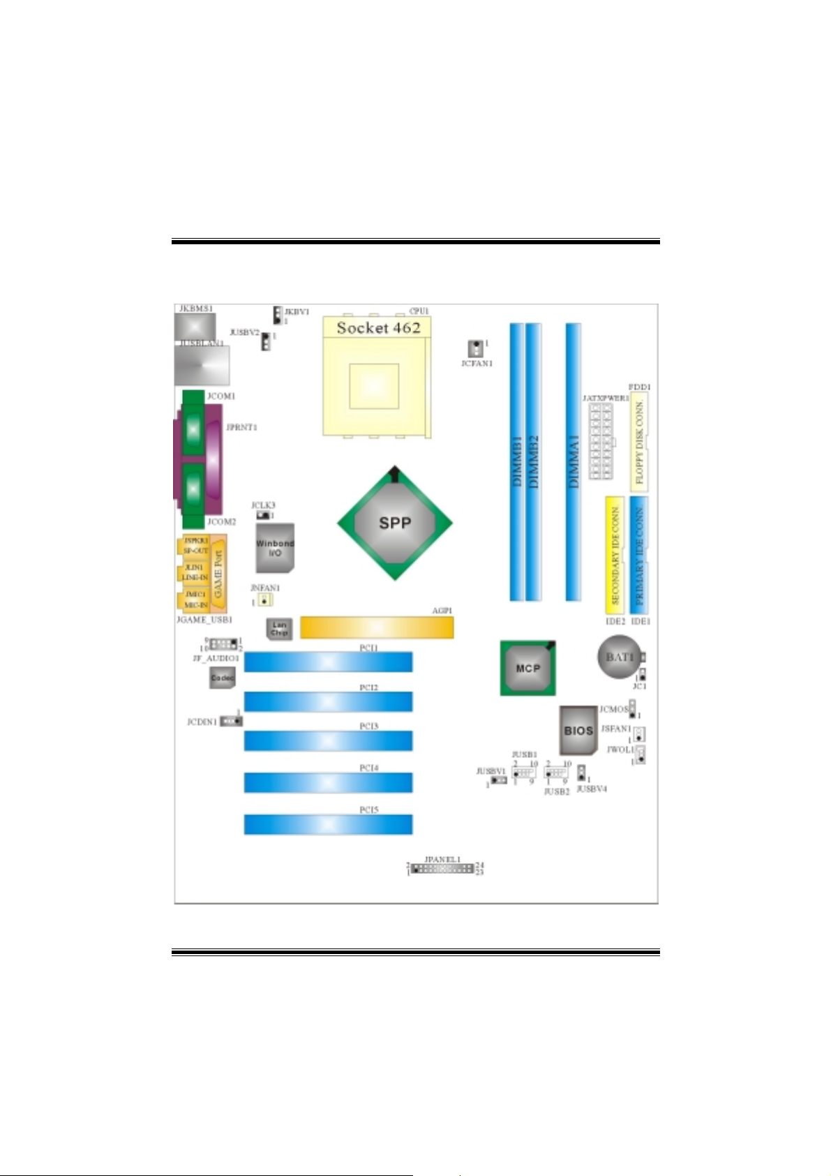
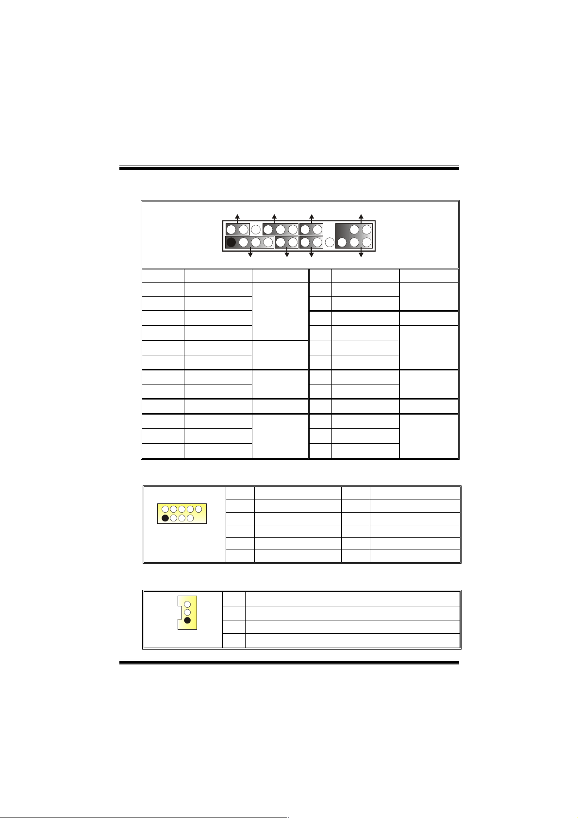
Layout of M7NCD Pro
※NOTE: ●represents the first pin.
1
Page 4
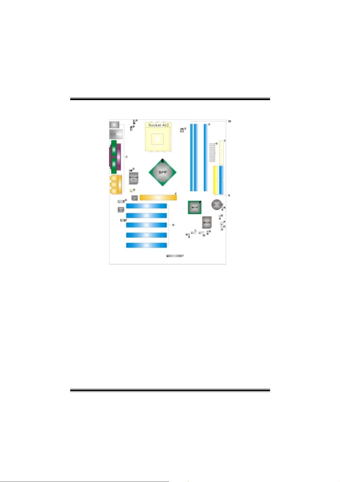
Component Index
A. 5V/5VSB Selection for Keyboard L. Front USB Header (JUS B1)
and mouse (JKBV1) M. Front USB Header (JUSB2)
B. Power Source Selection for USB N. Power Source Selection for USB
(JUSBV2) (JUSBV4)
C. Back Panel Connector O. Wake On LAN Header (JWOL1)
D. Frequency Selection (JCLK3) P. System FAN Header (JSFAN1)
E. North Bridge Fan Header (JNFAN1) Q. Clear CMOS Function (JCMOS)
F. Accelerated Graphics Port Slot R. Case Open Connector (JC1)
(AGP1) S. IDE Connectors (IDE1-2)
G. Front Audio Header (JF_AUDIO1) T. Floppy Disk Connector (FDD1)
H. PCI BUS Slots (PCI1-5) U. ATX Power Connector (JATXPWER1)
I. CD-ROM Audio-In Header (JCDIN1) V. DIMM Modules (DIMMA1)
J. Front Panel Connector (JPANEL1) W. DIMM Modules (DI MMB1-2)
K. Power Source Selection for USB X. CPU Fan Connector (JCFAN1)
(JUSBV1)
2
Page 5

English
M7NCD Pro Features
A. Hardware
CPU
Provides Socket-462.
Supports the AMD® processor up to XP 3200+.
Front Side Bus at 266/333/400 MHz.
Chipset
Nor th Br idge: nFORCE2 SPP.
South Bridge: MCP.
High Speed 800Mb/s Hyper-Transport interface to the MCP.
Main Memory
Supports up to 3 DDR devices.
Supports 266/333/400MHz (wi thout ECC) DDR devices.
High performance 128 bit DDR400 Twin Bank Memory Architecture.
Maximum memory size of 3GB.
Super I/O
Chip: Winbond W83627HF.
Slots
Five 32- PCI bus master slots.
One AGP: AGP3.0 8X interface at 533Mb/s.
Supports AGP 2X, 4X, 8X.
On Board IDE
Suppor ts four IDE disk drives.
Supports PIO Mode 4, Master Mode and Ultra DMA 33/66/100/133 Bus Master
Mode.
On Board AC’97 Sound Codec
Chip: ALC650.
Compliant with AC’97 specification.
AC99 2.2/2.3 interface.
Supports 6 channels.
On Board Peripherals
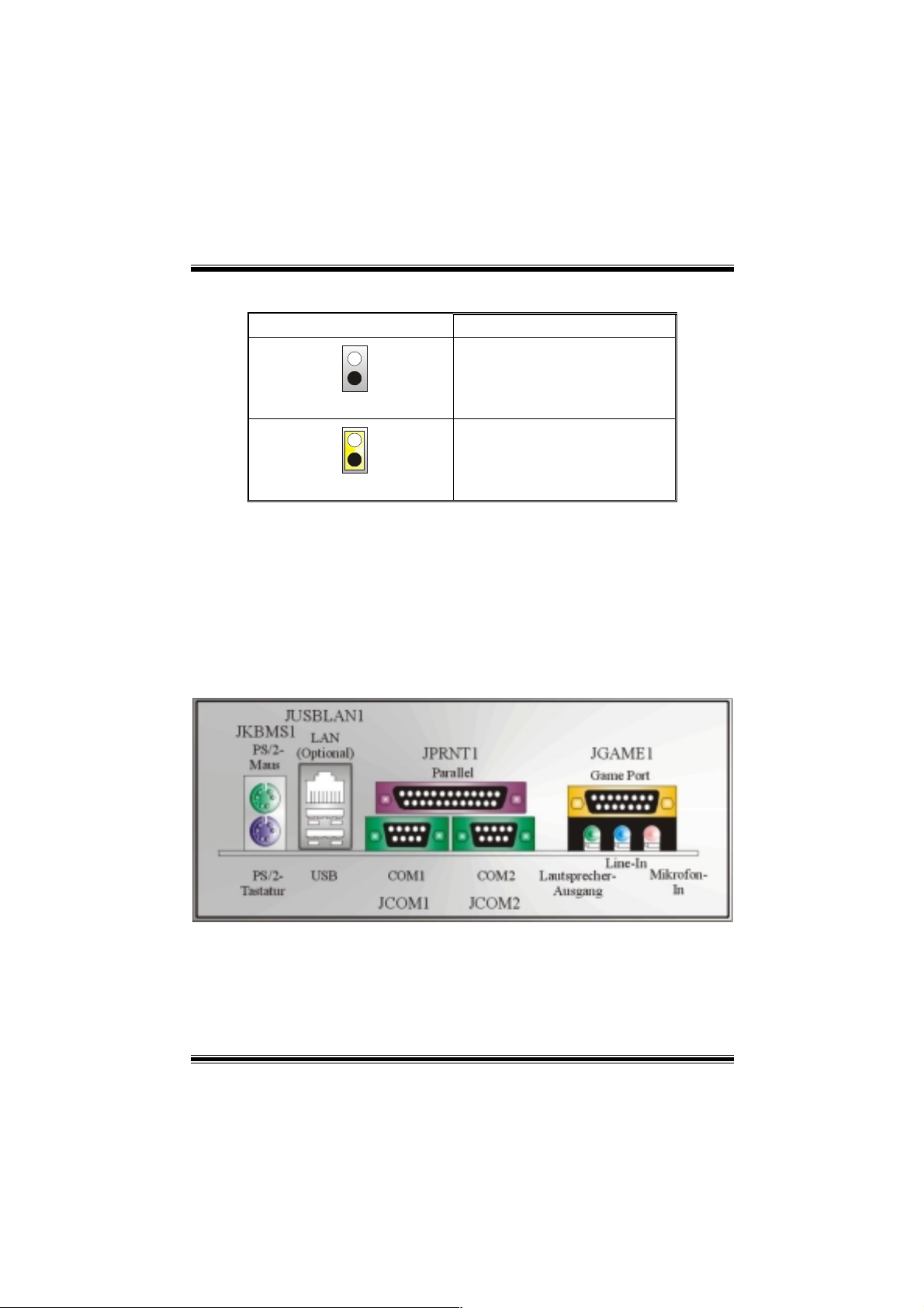
a. Rear side
2 serial ports.
1 parallel port. (SPP/EPP/ECP mode)
Audio ports in horizontal position.
1 LAN port. (optional)
3
Page 6
PS/2 mouse and PS/2 keyboard.
2 USB2.0 ports.
b. Front Side
1 floppy port supports 2 FDDs with 360K, 720K, 1.2M, 1.44M and 2.88Mbytes.
4 USB2.0 ports.
1 front audio header.
Dimensions
ATX Form Factor: 24.4cm X 30.4cm (W X L)
B. BIOS & Software
BIOS
Award legal Bios.
APM1.2.
ACPI.
USB Function.
Software
Supports CPU SaviorTM, 9th TouchTM, FLASHER™, WinFlasher
(optional) and Watchdog
Offers the highest p erformance for Windows 98 SE, Windows 2000, Windows Me,
Windows XP, SCO UNIX etc.
TM
.
TM
, StudioFun!
TM
Package contents
HDD Cable X1
FDD Cab l e X1
User’s Manual X1
USB Cable X1 (optional)
Rear I/O Panel for ATX Case X1 (opti onal)
Fully Setup Driver CD X1
StudioFun! Application CD X1 (optional)
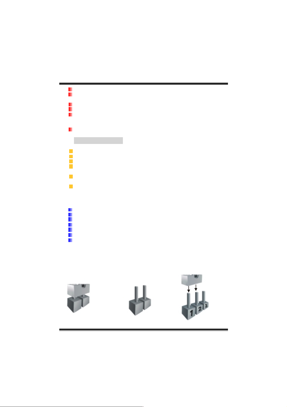
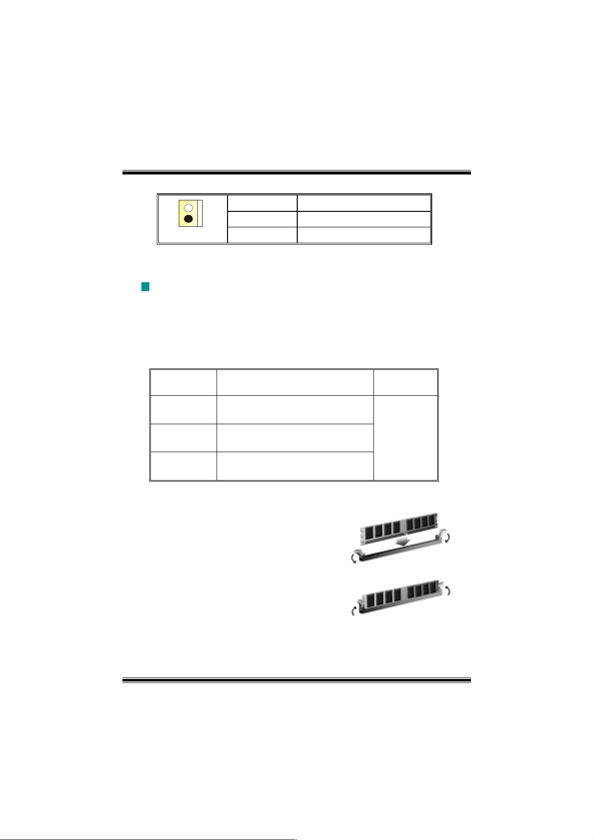
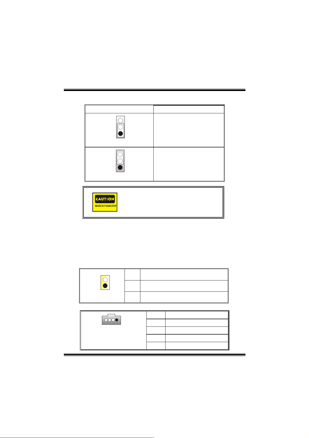
How to setup Jumper
The illustrati on shows how j umper s are set up. When the Jum per cap is place d on pin s, the
jumper is “close”. If no jumper cap is placed on the pins, the jumper is ”open”. The
illustration shows a 3-pin jumper whose pin 1and 2 are “close” when jumper cap is placed
on these 2 pins.
Jumper close Jumper open Pin1-2 close
4
Page 7
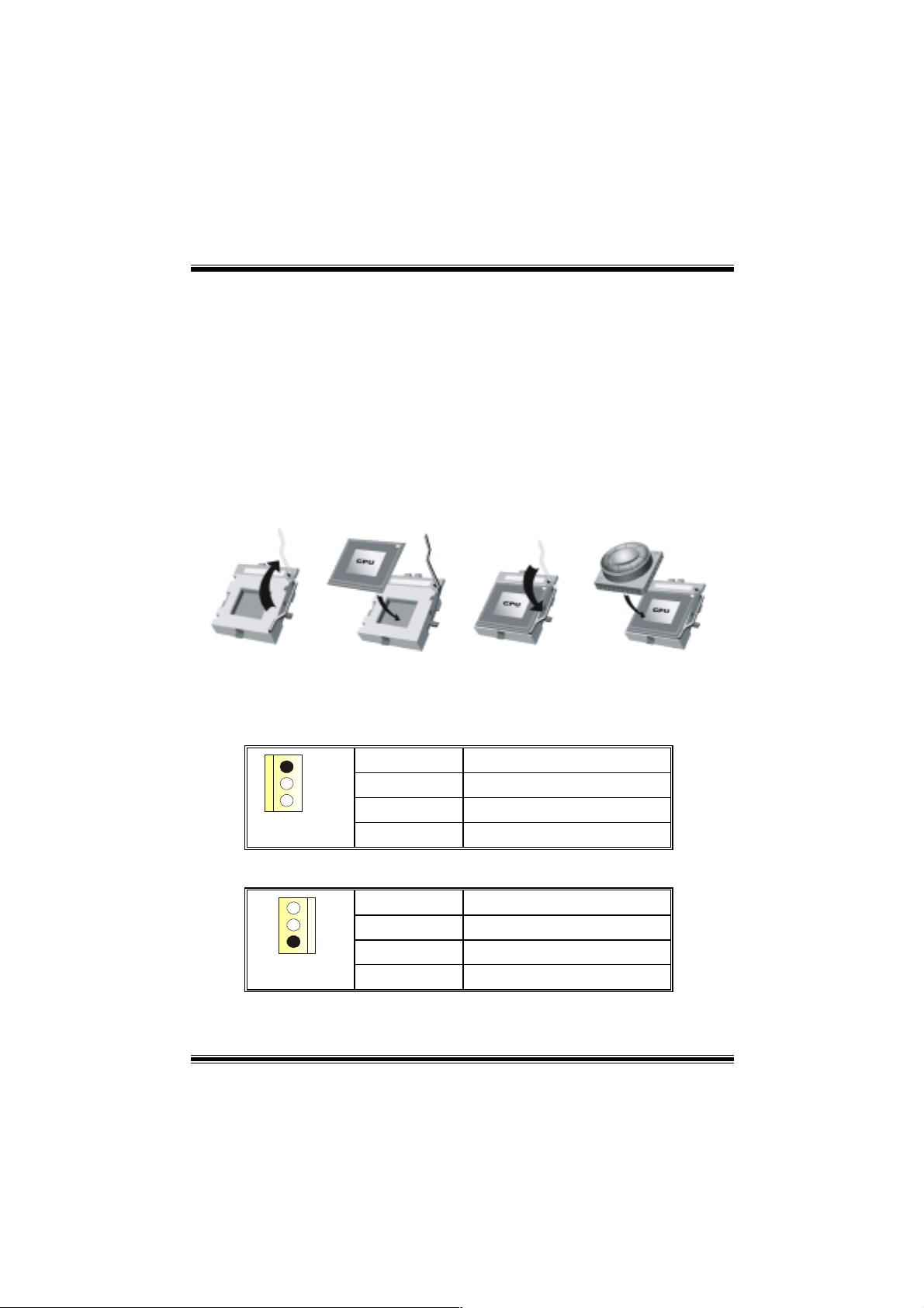
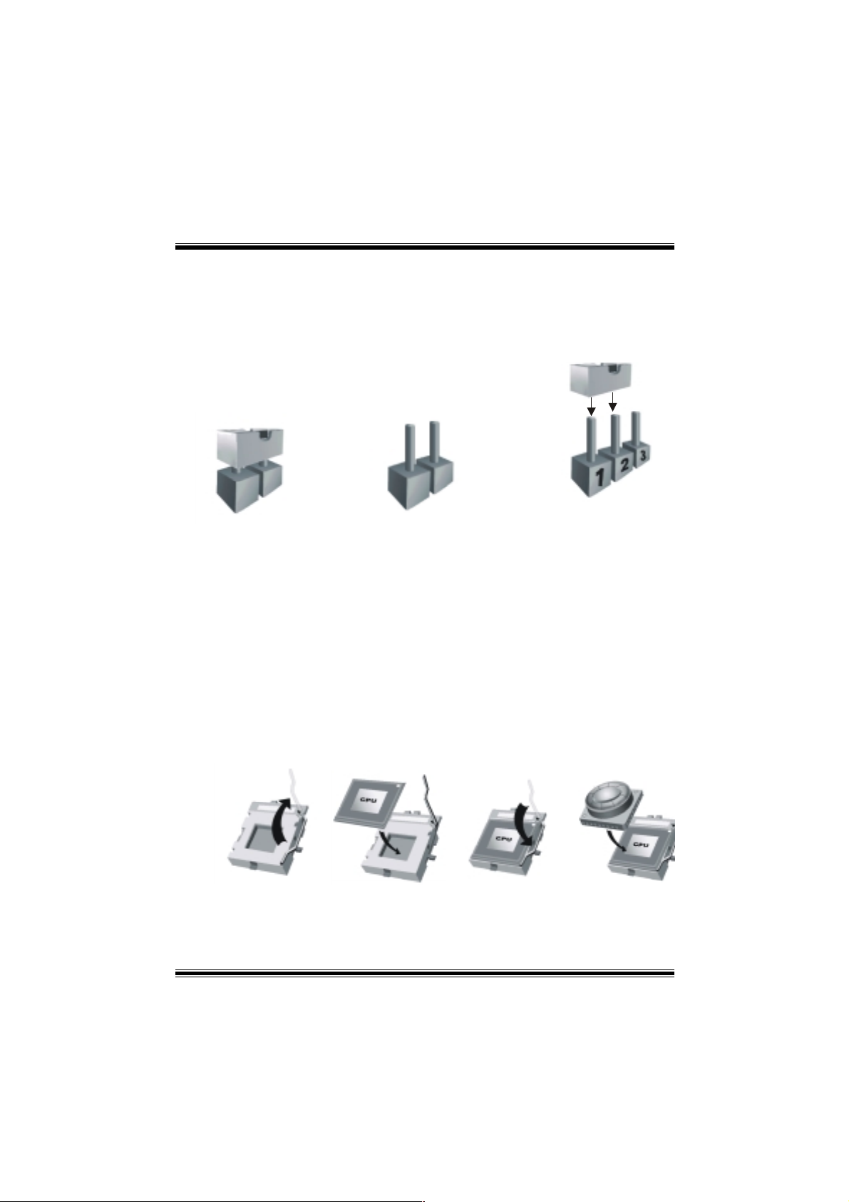
CPU Inst a l l ation
Step1:
Step2: Look for the whit e do t/cut edge. The white dot/cut edge should point towards the
Step3:
Step4: Put the CPU fan on the CPU and buckle it. Connect the CPU fan power cable to
Pull the lever sideways away from the socket and then raise the lever up to a
90-degree angle.
lever pivot. The CPU will fit only in the correct orientati on.
Hold the CPU down firmly, and then close the leve r.
the JCFAN1. This completes the installation.
Step1 Step2 Step3 Step4
CPU Fan Header: JCFAN1
1
JCFAN1
System Fan Head e r: JS F A N1
1
JSFAN1
Pin No. Assign ment
1
2
3
Ground
+12V
Sense
Pin No. Assign ment
1
2
3
5
Ground
+12V
Sense
Page 8
North Bridge Fan Header: JNFAN1
Pin No. Assign ment
1
JNFAN1
1
2
Ground
+12V
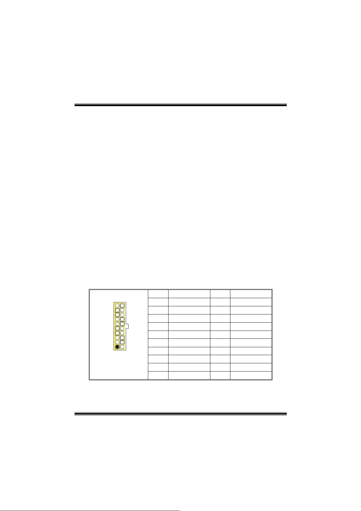
DDR DIMM Modules: DIMMB1-2, DIMMA1
For Dual-channel DDR (128-bit) high performance, at least 2 or more
DIMM modules must be installed. (It has to be the combination of
DIMMA and DIMMB.) With only one DIMM installed, the memory
performs only at 64-bit.
DRAM Access Time: 2.5V Unbuffered DDR 266/333/40 0 MHz Ty pe r equired.
DRAM Type: 64MB/ 128MB/ 256MB/ 512MB/ 1GB D IMM Module (184 p in)
Total Memory Size with Unbuffered DIMMs
DIMM Socket
Location
DIMMB1 64MB/128MB/256MB/512MB/1GB
DIMMB2 64MB/128MB/256MB/512MB/1GB
DIMMA1 64MB/128MB/256MB/512MB/1GB
Installing DDR Module
1. Unlock a DIMM slot by pressing the
retaining clips outward. Align a DIMM on
the slot such that the notch on the DIMM
matches the break on the slot.
2. Insert the DIMM firmly and vertically into
the slot until the retaining chip snap back in
place and the Dimm is properly seated.
DDR Module Total Me m or y
*1
*1
*1
***Only for re f e rence* **
Size (MB)
Max is
3GB
6
Page 9
Jumpers, Headers, Connectors & Slots
Floppy Disk Connector: FDD1
The motherboard provides a standard floppy disk connector that supports 360K,
720K, 1.2M, 1.44M and 2.88M floppy disk types. This connector supports the
provided floppy drive ribbon cables.
Hard Disk Connectors: IDE1/ IDE2
The motherboard has a 32-bit Enhanced PCI IDE Controller that provides PIO
Mode 0~4, Bus Master, and Ultra DMA 33/ 66/ 100/ 133 functionality. It has two
HDD connectors IDE1 (primary) and IDE2 (secondary).
The IDE connectors can connect a master and a slave drive, so you can connect
up to four hard disk drives. The first hard drive should always be connected to
IDE1.
Peripheral Component Interconnect Slots: PCI 1-5
This motherboard is equipped with 5 standard PCI slots. PCI stands for Peripheral
Component Interconnect, and it is a bus standard for expansion cards. This PCI
slot is designated as 32 bits.
Accelerated Graphics Port Slot: AGP1
Your monitor will attach directly to that video card. This motherboard supports
video cards for PCI slots, but it is also equipped with an Accelerated Graphics Port
(AGP). An AGP card will take advantage of AGP technology for improved video
efficiency and performance, especially with 3D graphics.
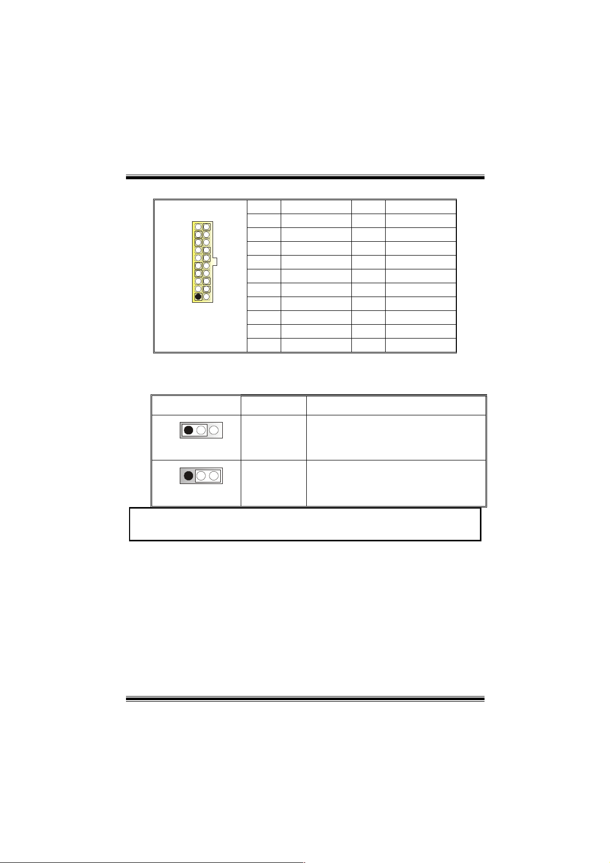
Power Connectors: JATXPWER1
PIN Assignment PIN Assignment
1 +3.3V 11 +3.3V
2 +3.3V 12 -12V
3 Ground 13 Ground
4 +5V 14 PS_ON
5 Ground 15 Ground
6 +5V 16 Ground
7 Ground 17 Ground
8 PW_OK 18 -5V
9 +5V_SB 19 +5V
10 +12V 20 +5V
10
1
JATXPWER1
20
11
7
Page 10
Front Panel C onnector: JPA NEL1
SLP
JPANEL1
Pin Assignment Function Pin Assignment Function
1
3
5
7
9
HDD LED (+)
11
HDD LED (-)
13
15
Reset Control
17
19
21
23
2
1
+5V
NA
NA
Speaker
Ground
NA
NA
+5V
IRTX
PWR_LED
(+) (-)(+)
SPK
Speaker
Connector
Hard Drive
LED
Reset
Button
IrDA
Connector
(+) (-)
HLED
RST
2
4
6
8
10
12
14
16
18
20
22
24
IRON/OFF
24
23
IR
Sleep Control
Ground
NA NA
Power LED (+)
Power LED (+)
Power LED (-)
Power Button
Ground
KEY
KEY
Ground
IRRX
Sleep
Button
POWER
LED
Power-on
Button
IrDA
Connector
Front USB Header: JUSB1/2
2
1
JUSB1/2
Pin Assignment Pin Assignment
10
1
3
9
5
7
9
+5V(fused)
USBP4-
USBP4+
Ground
KEY
2
4
6
8
10
+5V(fused)
USBP5-
USBP5+
Ground
NA
Wake On LAN Header: JWOL1
Pin Assignment
1
JWOL1
1
2
3
+5V_SB
Ground
Wake up
8
Page 11
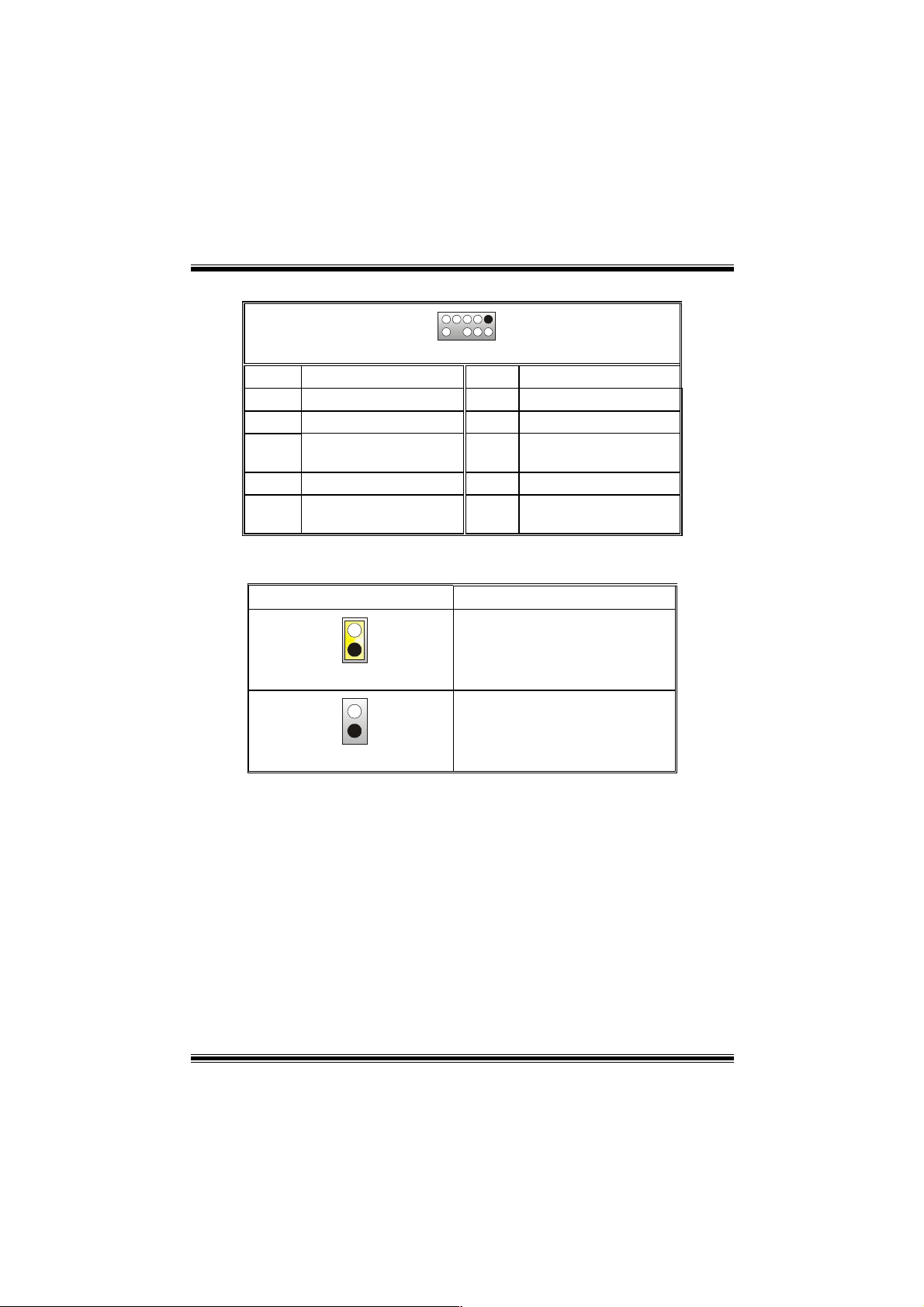
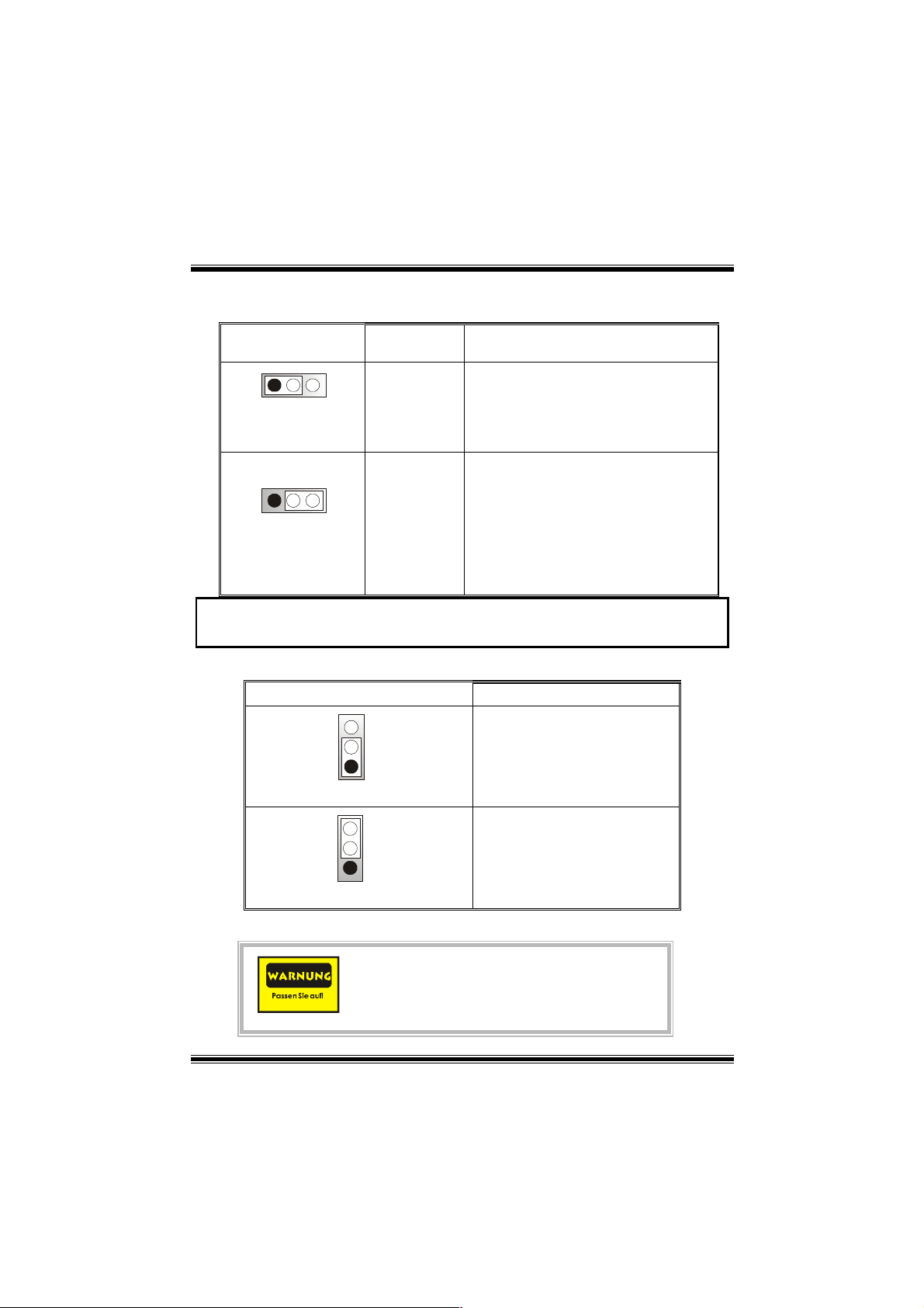
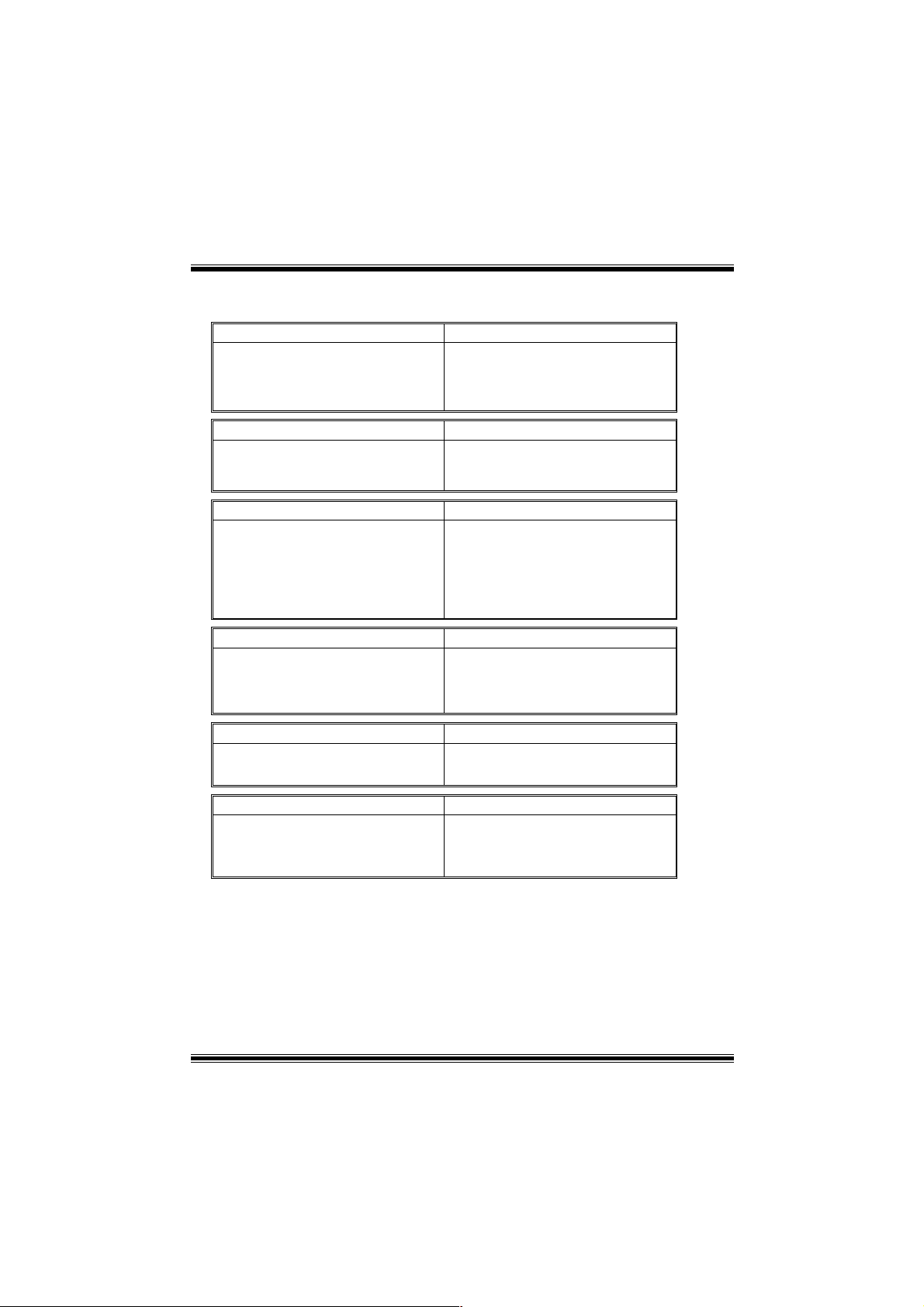
Power Source Selection for Keyboard/ Mouse: JKBV1
JKBV1 Assignment Description
3
1
Pin 1-2 close
3
1
Pin 2-3 close
+5V
+5V Standby
Voltage
+5V for keyboard and mouse
PS/2 Mouse and PS/2 Keyboard are
powered with +5V standby voltage
Note: In order to power-on keyboard and mouse function, “JKBV1” jumper
cap should be placed on pin 2-3.
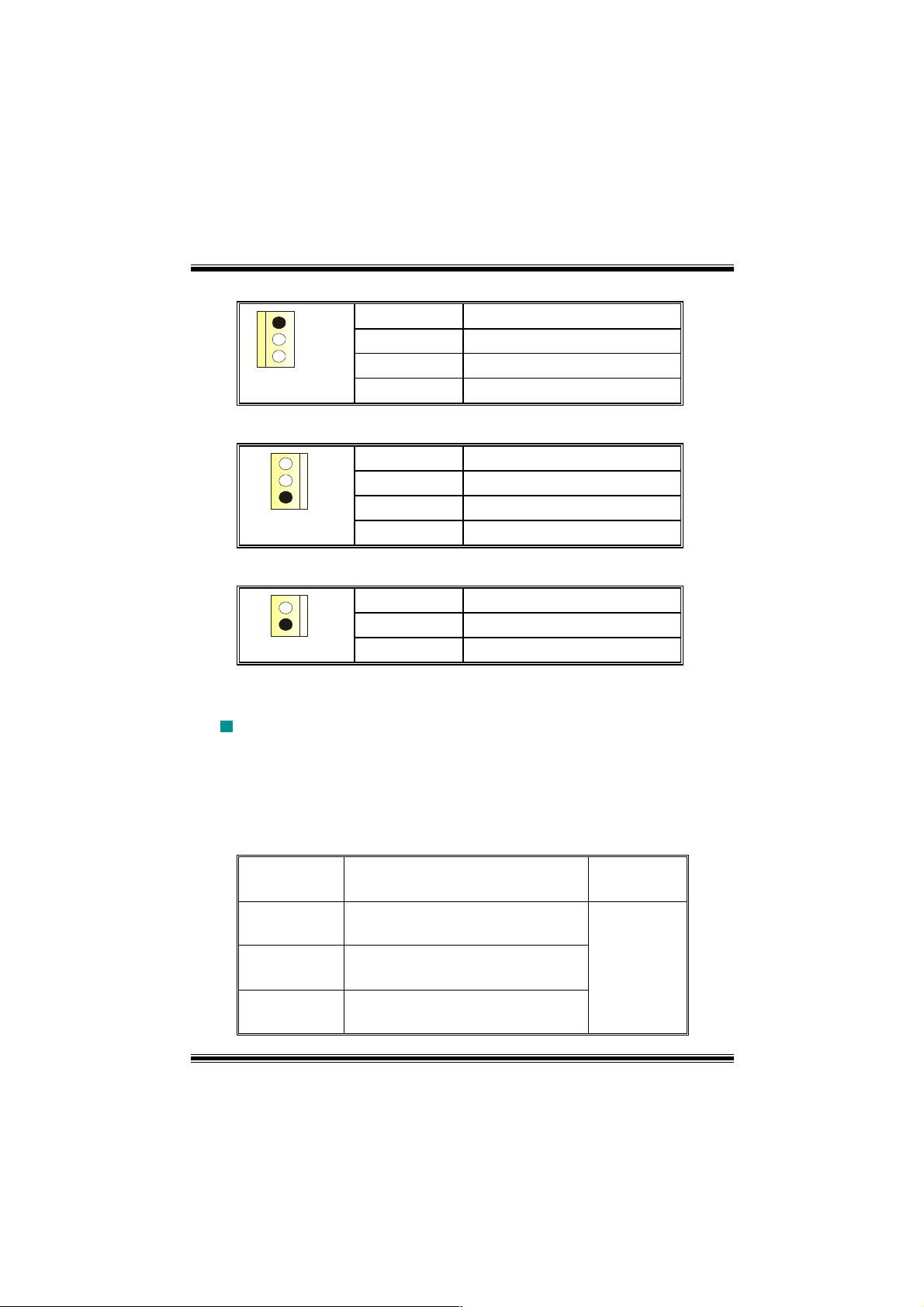
Power Source Selection for USB: JUSBV1/ JUSBV2/ JUSBV4
JUSBV1/JUSBV2/
JUSBV4
1 3
Pin 1-2 close
1 3
Pin 2-3 close
Assignment Description
+5V Standby
+5V
Voltage
JUSBV1: 5V for JUSB1 port
JUSBV2: 5V for JUSBLAN1 port
JUSBV4: 5V for JUSB2 port
JUSBV1: JUSB1 port powered with
standby voltage of 5V
JUSBV2: JUSBLAN1 port powered with
standby voltage of 5V
JUSBV4: JUSB2 port powered with
standby voltage of 5V
Note: In order to power-on USB devices function, “JUSBV1/JUSBV2/
JUSBV4” jum per cap sho uld be pla ce d on pi n 2- 3 r es p ec t iv e ly .
9
Page 12
Clear CMOS Jumper: JCMOS
JCMOS Assignment
3
1
Pin 1-2 Close
3
1
Pin 2-3 Close
The following procedure s are for resetting the
BIOS password. It is important to follow these
instructions closely.
※ Clear CMOS Procedures:
1. Remove AC power line.
2. Set the jumper to “Pin 2-3 Close”.
3. Wait for five seconds.
4. Set the jumper to “Pin 1-2 Close”.
5. Power on the AC.
6. Reset your desired password or clear the CMOS data.
Case Open Connector: JC1
Pin
Normal Operation (default)
Clear CMOS Data
Assignment
1
JC1
1
2
Case Open Signal
CD-ROM Audio-In Header: JCDIN1
Pin Assignment
1
2
3
4
10
JCDIN1
1
Ground
Left Channel Input
Ground
Ground
Right Channel Input
Page 13
Front Panel Audio Header: JF_AUDIO1
9
10
JF_AUDIO1
Pin Assignment Pin Assignment
1
3
5
7
9
Mic In/ Center
Mic Power/ Bass
Right Line Out/ Speaker
Out Right
Reserved
Left Line Out/ Speaker
Out Left
2
2
4
6
8
10
1
Ground
Audio Power
Right Line Out/ Speaker
Out Right
Key
Left Line Out/ Speaker
Out Left
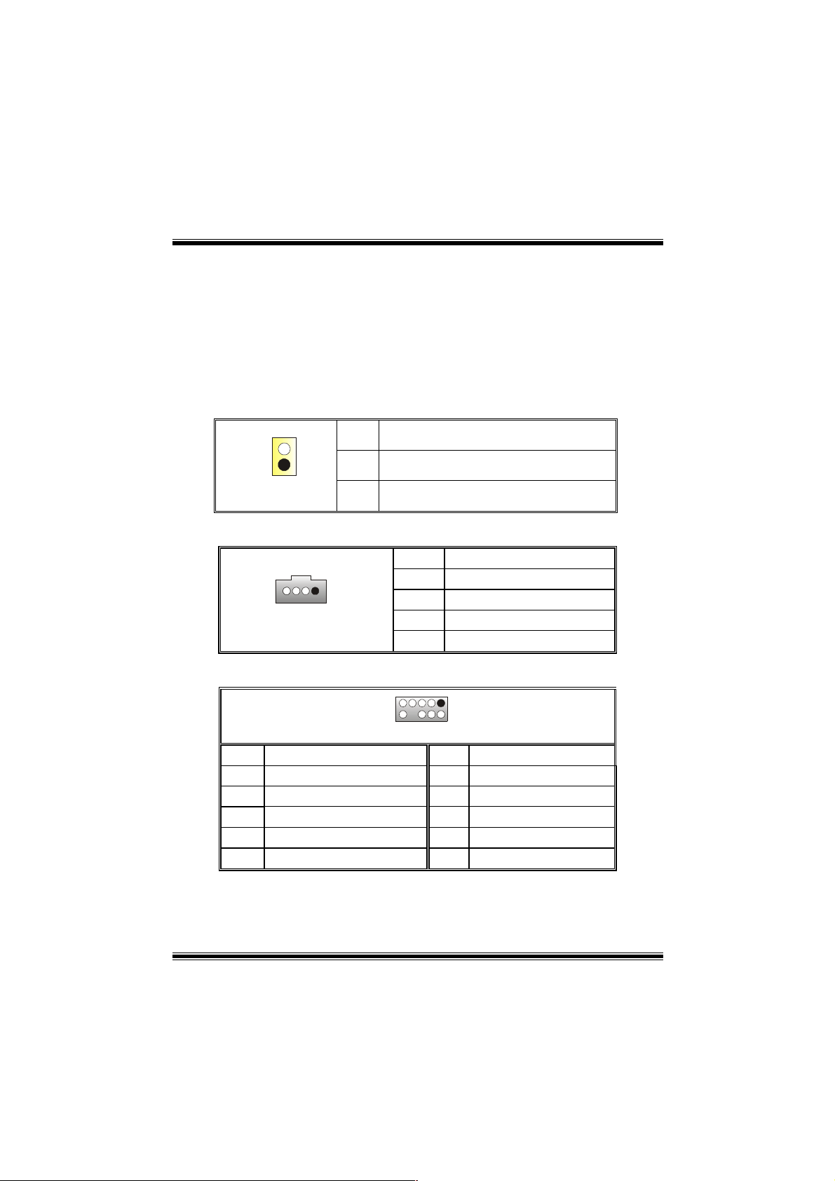
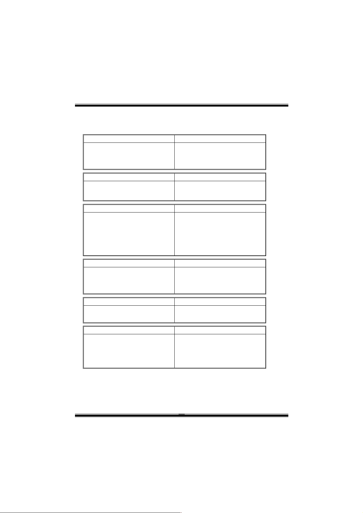
System Operation Mode: JCLK3
Note: W hen overclock function failed and system is unable to boot-up, please
follow the instruction below:
1. Turn off the system.
2. Closed the JCLK3 jumper.
3. Turn on the system.
4. Enter CMOS setup menu and load defaults settings.
5. Turn off the system.
6. Open the JCLK3 jumper.
7. Turn on the system.
JCLK3 Assignment
1
Pin 1-2 Close
1
Pin 1-2 Open
User Mode (default)
(133/ 166 MHz)
Safe mode
(100 MHz)
11
Page 14

Back Panel Connectors
12
Page 15

Deutsch
Spezifikationen von M 7NCD Pro
A. Hardware
CPU
Unterstützung für Sockel 462.
Unterstützung für den AMD® Prozessor bis zu XP 3200+.
FSB mit 266/333/400 MHz.
Chipsatz
Northbridge: nFORCE2 SPP.
Southbridge: MCP.
Hauptspeicher
Unterstützung für 3 DDR Geräte.
Unterstützung für 266/333/400MHz (ohne ECC) DDR Geräte.
128-Bit High-Performance DDR400 mit der Twin-Bank Architektur.
Die maximale Spei chergröße ist 3GB.
Super I/O
Chip: Winbond W83627HF.
Slots
Fünf 32-Bit PCI-Bus-Slots.
Ein AGP-Slot: AGP3.0 8X Interface bei 533Mb/s.
Unterstützung für AGP2.0 2X , 4X und 8X.
Onboard-IDE
Unterstützung für vier IDE Diskettenlaufwerke.
Unterstützung für PIO Modus 4, Master Modus und Ultra DMA 33/66/100/133 Bus
Master Modus.
On-board AC ’97 Sound Codec
Chip: ALC650.
Entspricht die Spezifikation von AC’97.
AC99 2.2/2.3 Interface.
Unterstützung für 6-Kanal.
Onboard-Peripheriegeräte
a. Rückwand
2 Seriell-Ports.
1 parallele Schnittstelle. (SPP/EPP/ECP-Modus)
1 horizontales Audio-Port.
1 LAN-Port. (optional)
Unterstützung für PS/2-Maus und PS/2-Tastatur.
13
Page 16

2 USB2.0-Ports.
b. Vorderseite
1 Floppy-Port mit Unterstützung für 2 Diskettenlaufwerke.(360KB, 720KB, 1.2MB,
1.44MB und 2.88MB)
4 USB2.0-Ports.
1 Audio-Header für die Vonderseite
Abmessungen
ATX Form-Facto r: 24 .4 X 30.4 c m (W X L)
B. BIOS & Software
BIOS
Award legal Bios.
APM1.2.
ACPI.
USB Funktion.
Software
Unterstützung für CPU SaviorTM, 9th TouchTM, FLASHER™, WinFlasherTM,
StudioFun!
Unterstützung für die am meisten verbreiteten Betriebsysteme wie Windows 98SE,
Windows 2000, Windows ME, Windows XP and SCO UNIX usw.
TM
(optional) and WatchdogTM.
Verpackungsinhalt
HDD Kable X1
FDD Kable X1
Benutzer Handbuch X1
USB Kable X1 (optional)
I/O-Rückwand für ATX Gehäuse X1 (optional)
Treiber CD für Installation X 1
StudioFun! Anwendung CD X1 (optional)
14
Page 17
Einstellung der Jumpe r
Die Abbildung verdeutlicht, wie Jumper eingestellt werden. Pins werden durch die
Jumper-Kapp e verdeck t, ist de r Jumper ”geschlossen”. Keine Pins werden durch die
Jumper-Kappe verdeckt, ist der Jumper “geöffnet”. Die Abbiildung zeigt einen 3-Pin
Jumper dessen Pin1 und Pin2 ”geschlossen“ sind, bzw. es befindet sich eine
Jumper-Kappe auf diesen beiden Pins.
Jumper geschlossen Jumper geöffnet Pin1-2 geschlossen
Installation der CPU
Schritt 1: Ziehen Sie den Heb el seitlich vom Sockel weg. Heben Si e den Hebel dann
in 90-Grad-Winkel nach oben.
Schritt 2: Suchen Sie nach der scharfen Kante, die auf Drehpunkt des Hebels
weisen muss. Die CPU passt nur, wenn sie richtig ausgerichtet ist.
Schritt 3:
Schritt 4:
Drücken Sie die CPU fest in den Sockel und schließen Sie den Hebel.
Stecken Sie Ihren CPU-Lüfter auf die C PU. Schließen Sie di e Stromversorgungsstecker
für CPU-Lüfter an JCFAN1 an. Dann beenden Sie die Installation.
Schritt 1 Schritt 2 Schritt 3 Schritt 4
15
Page 18
CPU-Lüfter Headers: JCFAN1
1
Pin
1
JCFAN1
2
3
Belegung
Masse
+12V
Sensor
System-Lüfter Headers: JSFAN1
Pin
1
1
JSFAN1
2
3
Northbridge-Lüfter Header: JNFAN1
Pin
1
JNFAN1
1
2
Belegung
Masse
+12V
Sensor
Belegung
Masse
+12V
DDR-DIMM-Modules: DIMMB1-2, DIMMA1
Für Dual-Kanal DDR (128-Bit) High-Performance, muss man mindestens
2 oder mehr DIMM-Module installieren. (Es ist unbedingt, daß man DIMMA
mit DIMMB als ein Paar benutzt.) Wenn man nur ein DIMM installiert,
funktioniert der Spreicher nur 64-Bit.
DRAM-Zugriffszeit: 2.5V nicht registrierter DDR 266/333/400 MHz Typ
erforderlich.
DRAM Typen: 64MB/ 128MB/ 256MB/ 512MB/ 1GB DIMM-Module (184-Pin)
Gesamt Speichergröße von nicht registrierter DIMMs
DIMM-Sockel
Standort
DIMMB1 64MB/128MB/256MB/512MB/1GB
DIMMB2 64MB/128MB/256MB/512MB/1GB
DIMMA1 64MB/128MB/256MB/512MB/1GB
DDR-Modul Speichergröße
*1
maximal
*1
*1
**Nur als Referenz***
16
3GB
Page 19

Installation von DDR-Modul
1. Öffnen Sie einen DIMM-Slots, indem Sie
die seitlich Chips nach außen drücken.
Richten Sie das DIMM-Modul so über dem
Slot aus, dass das Modul mit der Kerbe in
den Slot passt.
2. Drücken Sie das DIMM-Modul in den Slot,
bis die seitlichen Clips zuschnappen und
das Modul fest sitzt.
Jumpers, Headers, Anschlüsse & Slots
Diskettenanschluss: FDD1
Das Motherboard enthält einen standardmäßigen Diskettenanschluss, der 360K-,
720K-, 1.2M-, 1.44M- und 2.88M-Disketten unterstützt. Dieser Anschluss
unterstützt die mitgelieferte Bandkabel des Diskettenlaufwerks.
Festplattenanschlüsse: IDE1 und IDE2
Das Mainboard hat einen 32-Bit Enhanced PCI IDE-Controller, der die Modi
PIO0~4, Bus Master sowie die Ultra DMA/33/66/100/133- Funktion zur Verfügung
stellt. Dieser ist mit zweii HDD-Anschlüssen versehen IDE1 (primär) und IDE2
(sekundär).
Die IDE-Anschlüsse können eine Master- und eine Slave-Festplatte verbinden, so
dass bis zu 4 Festplatten angeschlossen werden können. Die erste Festplatte
sollte immer an IDE1 angeschlossen werden.
Peripheral Component Interconnect Slots: PCI1-5
Dieses Motherboard ist mit 5 standardmäßigen PCI-Slots ausgestattet. PCI steht
für Peripheral Com pone nt Int erconn ect und bezi eht sich au f einem Bussta ndard für
Erweiterungskarten, der den älteren ISA-Busstandard in den meisten
Schnittstell en ersetzt hat. Dieser PC I-Slot ist für 32 bits vorgesehen.
Accelerated Graphics Port Slot: AGP1
Ihr Monitor wird direkt an die Grafikkarte angeschlossen. Dieses Motherboard
unterstützt Grafikkarten für PCI-Slots, aber es ist auch mit einem Accelerated
Graphics Port ausgestattet. AGP-Karten verwenden die AGP-Technologie, um die
Wirksamkeit und Leistung von Videosignalen zu verbessern, besonders wenn es
sich um 3D-Grafiken handelt.
17
Page 20
Anschlüsse für die Vorderseite: JPANEL1
SLP
JPANEL1
Pin Belegung Funktion Pin Belegung Funktion
1
3
5
7
9
11
13
15
17
19
21
23
2
1
+5V
Kein
Kein
Lautsprecher
HDD LED (+)
HDD LED (-)
Masse
Reset Control
Kein 18Schlüsse Kein Pin
Kein
+5V
IRTX
PWR_LED
(+) (-)(+)
SPK
Lautsprecher
Anschluss
Festplatte
LED
Zurücksetzn-
Knopf
IrDA-
Anschluss
(+) (-)
HLED
RST
2
Sleep Control
4
6
8
Power LED (+)
10
Power LED (+)
12
Power LED (-)
14
Power-Knopf
16
20
22
24
IRON/OFF
24
23
IR
Schlafen-
Masse
Kein Kein
Masse
Schlüsse
Masse
IRRX
Knopf
Power-
LED
Power-On
Knopf
IrDA
Anschluss
Front USB Header: JUSB1/2
2
1
JUSB1/2
10
9
Pin
1
3
5
7
9
Belegung
+5V(geschmelzt)
USBP4-
USBP4+
Masse
Schlüsse
Pin
2
4
6
8
10
Belegung
+5V(geschmelzt)
USBP5-
USBP5+
Masse
Kein
Wake On LAN Header: JWOL1
1
JWOL1
Pin
1
2
3
Belegung
+5V_SB
Masse
Wake-up
18
Page 21
Stromversorgungsanschluss: JATXPWER1
10
20
1
11
JATXPWR1
PIN Belegung PIN Belegung
1 +3.3V 11 +3.3V
2 +3.3V 12 -12V
3 Masse 13 Masse
4 +5V 14 PS_ON
5 Masse 15 Masse
6 +5V 16 Masse
7 Masse 17 Masse
8 PW_OK 18 -5V
9 +5V_SB 19 +5V
10 +12V 20 +5V
Auswahl von Stromversorg ungsmodi für Tastatur/ Maus:
JKBV1
JKBV1 Beschreibung Funktion
1 3
Pin 1-2
geschlossen
1 3
Pin 2-3
geschlossen
+5V
+5V reserviert e
Spannung
PS/2-Maus und PS/2-Tastatur werden durch
5V für Tastatur und Maus
5V reservierte Spannung aktiviert
Anmerkung: Um die “power-on by Keyboard and Mouse“ Funktion zu
behandeln, sollen Pin2-3 durch die Jumperkappe verdeckt werden.
19
Page 22
Auswahl von Stromsversor gungsmodi für USB: JU SBV 1/
JUSBV2/JUSBV4
JUSBV1/JUSBV2/
JUSBV4
Beschreibung Funktion
1 3
Pin 1-2 geschlossen
1 3
Pin 2-3 geschlossen
+5V
+5V_SB JUSBV1: JUSB1 ist aktiviert durch
JUSBV1: 5V für JUSB1
JUSBV2: 5V für JUSBLAN1
JUSBV4: 5V für JUSB2
die reservierte 5V Spannang
JUSBV2: JUSBLAN1 ist aktiviert
durch die reservierte 5V Spannang
JUSBV4: JUSB2 ist aktiviert durch die
reservierte 5V Spannang
Anmerkung: Um die “power-on by USB-Geräte” Funktion zu behandeln,
sollen pin2-3 von JUBV1/ JUBV2/ JUSBV4 durch die.
Jumper zum Löschen CMOS: JCMOS
JCMOS
3
1
Pin 1-2 geschlossen
3
1
Pin 2-3 geschlossen
Die folgende Schritte leit en Si e, d as K ennw ort für
BIOS-System zurückzusetzen. Es ist wichtig, die
Anweisung zu folgen.
Beschreibung
Normale Operation (Default)
CMOS-Daten Löschen
20
Page 23
※ Prozeß zum Löschen des CMOS:
1. Ausschalten Sie den AC-Netzstecker.
2. Lassen Sie Pin 2-3 von JCOMS1 geshclossen sein.
3. Bitte warten Sie 15 Sekunden.
4. Lassen Sie Pin 1-2 von JCOMS1 geshclossen sein.
5. Schließen Sie den AC-Netzstecker an.
6. Zurücksetzen Sie das Kennwort nach ihrem Wille oder löschen
Sie die CMOS-Daten.
Anschluss für Gehäuse-Öffnen : JC1
Pin
Belegung
1
JC1
1
2
Gehäuse Öffnen Signal
Masse
CD-ROM Audio-In Header: JCDIN1
1
JCDIN1
Pin Belegung
1
2
3
4
Link-Kanal Eingabe
Masse
Masse
Recht-Kanal Eingabe
Front Panel Audio Header: JF_AUDIO1
9
10
JF_AUDIO1
Pin Belegung Pin Belegung
1
3
5
7
9
*Reserviert: Nicht i n Gebrauch
Mikrofon-Eingang
Mikrofon-Betriebsspannung
Recht Line-Out
Reserviert
Link Line-Out
2
4
6
8
10
1
2
Audio-Spannung
Recht Line-Out
Link Line-Out
Masse
Schlüsse
21
Page 24
System Operat ion Modus: JCLK3
Anmerkung: Wenn “Überspanng Funktion” nicht gelungen ist folgen Sie bitte
die Instruktion darunter:
1. Bitte vausschalton Sie den AC-N otzstecker.
2. Lassen Sie Pin 1-2 von JCLK3 geschlossen sein.
3. Schließen Sie den AC-Notzstecker an.
4. Betreten Sie “CMOS Setup Menü” und wählen sie Default-Setting.
5. Ausschalten Sie den AC-Netzstecker wieder.
6. Lassen Sie Pin 1-2 von JCLK3 geöffnet sein.
7. Schließen Sie den AC-Netzstecker wieder.
JCLK3 Assignment
1
Pin 1-2 Geöffnet
1
Pin 1-2 Geschlossen
Benutzer Modus (default)
(133/ 166 MHz)
Sicherheit Modus
(100 MHz)
Anschlüsse für die Rückwand
22
Page 25

Watchdog Technology
It is important to know that when overclocking, the system can be at a vulnerable state.
Therefore, the BIOSTAR Watchdog Technology was designed to protect your PC under
dangerous over-clock situations. Any over-clocking that reaches the threshold settings,
the Watchdog Technology will disable your system from rebooting in the BIOS setting.
Under this cir cumstance, please power off your PC. After that, press <Insert> and pow er
on your system simultaneously to restart your system. This user-friendly design can
save you from squan deri ng y our tim e on ope ni ng the cas e just to clear the CM OS. In the
end, thanks to the Watchdog Technology, everything is back at a safe and sound!
23
Page 26

StudioFun!
Introduction
StudioFun! is a media-player based on optimized GNU/Linux distribution. It plays DVD,
VCD, MP3, Audio CD and various other known file formats. You can take snapshots of
video and customize the saved images as screensavers. You can also store the images
on USB mass storage devices like flash disks and USB floppy disks.
Hardware Requirement s
The supported hardware list of StudioFun! grows up every day. So please check the
hwreq.txt located in the root of StudioFun! Installation CD to get the most updated
information.
Installation Procedure
Insert the StudioFun! Installation CD in a CD/DVD ROM drive and let the system boot
through the CD. The disk will boot and bring up the grub boot loader installation menu.
Two options are specified.
24
Page 27

Installation
This option will do the basic installation of the distribution. The installation works on
pre-installed windows or GNU/Linux distribution.
On selecting the ’i nsta ll ation’ option the instal ler boots and di spl ay s a di alo g box indi cati ng
the space required and waits for a confirmation. Selecting Ok will continue the installation
while selecting Cancel will terminate the installation and reboot the machine.
If Windows or GNU/Linux is the only OS installed on the hard disk with no free space, it
will resize the partition, either NTFS or FAT32 or ext2, and install StudioFun!. In case the
hard disk has a 128MB of free space available, the installation will use the free space.
After installing the base system you will be prompted to select the resolution from the
following choices
1. 1024x768 (recommended)
2. 800x600
3. 640x480
Select the desired resolution. The default is 1024x768 for high- end graphics.
Next you will be prompted to choose the DVD area/region selection code. Choose this
based on the type of DVDs you will be playing.
The installation procedure will then probe for the type of mouse installed. The distribution
currently supports PS/2, USB and Serial mice. In case of serial mouse you will have to
move the mouse when prompted. The other two are probed and installed automatically.
The installation procedure will now finish, the CD is ejected and a dialog box prompting to
reboot the machine is displayed. Press OK button and enjoy StudioFun!.
3.1.1 Error Messages
1. Media corrupted!! Please check the media! The CD-ROM is corrupted.
2. Extraction of base sy stem failed!! Please try again later!! The CD-ROM is corrupted.
3. Unsupported hardware found, Aborting... If you try to install StudioFun! on an
unsupported and undocumented hardware the above error message is popped.
4. No device found! This error message is given if there is no hard disk in the system.
25
Page 28

Recovery
In case of a MBR corruption, this option should be used. It will automatically probe the
hard disk master boot record and find out the installed operating system(s). On success it
will re-install the boot loader with correct options in the MBR. Any custom boot loader
option specified from other GNU/Linux installations will get over written by the newly
probed one.
Booting to StudioFun!
After Installation is over, remove the CD from the CD-ROM and restart the machine. After
the machine reboots, you will get the GRUB boot loader menu screen. Select the
StudioFun option to boot to the StudioFun! partition.
26
Page 29

After complete boot up, you get to the main Desktop screen. The following section is
a complete description of the Desktop application.
Desktop
This is the main shell of the StudioFun software. It basically comprises of two categories,
one is the main "media control" part and the other is the "control panel".
Media control
The media control part of the Desktop has the following controls:
1. VCD
This control will glow whenever a VCD is detected in a DVD/CD-ROM drive. The VCD will
be auto-played onl y wh en i t is put i n to the dr ive when th e D eskto p (St udi oFun ! sh el l ) i s up
and running, otherwise, the control will simply glow to inform the user about a VCD
27
Page 30

present in the DVD/CD-ROM drive.
2. DVD
This control will glow whenever a DVD is detected in a DVD drive. The DVD will be
auto-played only when it is put in to the drive when the Desktop (StudioFun! shell) is up
and running, otherwise, the control will simply glow to inform the user about a DVD
present in the DVD/CD-ROM.
3. MP3
This control will glow whenever a MP3 is detected in a DVD/CD-ROM drive. The MP3 will
be auto-played onl y wh en i t is put in to the drive when the De skto p (StudioFun! shel l) is up
and running, otherwise, the control will simply glow to inform the user about a MP3
present in the DVD/CD-ROM drive.
4. AUDIO
This control will glow when ever a AUDIO is d etect ed in a DVD/ CD-ROM dri ve. The AUDIO
will be auto-played only when it is put in to the drive when the Desktop (StudioFun! shell)
is up and running, otherwise, the control will simply glow to inform the user about a AUDIO
present in the DVD/CD-ROM drive.
5. FILE
This control will glow whenever a File CD (CDs with other media type files) is de tected in a
DVD/CD-ROM drive. The File CD will be auto-played only when it is put in to the drive
when the Desktop (StudioFun! shell) is up and running, otherwise, the control will simply
glow to inform the user about a Fil e CD present in the DVD/CD- ROM drive.
6. EJECT MEDIA
This control when clicked will eject any MP3 or File CDs from any of the DVD/CDROM
drives. In case there were no MP3 or File CDs it will eject the default medium, (i.e.), the
CD-ROM drive in case if the user has both DVD/CD-ROM drive or else it will eject the
default DVD/CD-ROM drive.
7. EXIT
This is the "Power on/off" control of the Desktop (StudioFun! shell).
Control Panel
Control panel part has five icons, which are shortcuts to other applications present in the
StudioFun software. Tool tips are provided on the icons when the mouse is rolled over
them.
28
Page 31

1. Select Region
Clicking this icon will invoke the application for selection DVD region settings. Refer to
section 5.2 Select DVD Region application for more details.
2. Screensaver
Clicking this icon will invoke the screensaver application. Refer to section 5.3
Screensaver
for more details .
3. Display Settings
Clicking this icon will invoke the application for changing the screen resolutions. Refer to
section 5.4, Display Settings for more details.
4. File Manager
Clicking this icon will invoke the file manager. Refer to section 5.6 File manager for more
details.
When user has a DVD and a CD-ROM Drive:
If user has both DVD and a CD-ROM drive, DVD drive will be given the preference when
both the drives h ol d valid media in them, i.e., if the CD-ROM dri ve ha s a me dia and a DVD
drive also has a media, and the StudioFun! is started, then the media inside the DVD drive
will be played.
If in case the media in CD-ROM takes a longer time to get recognized than the media
inside the DVD drive, the media in the CD-ROM will be played, once if it is recognized.
Other general user scenarios
When a user clicks on any of t he m edi a-c ontrols when it i s n ot gl owi ng, ex cept ej ect m e di a
and exit, the media-player will just come up and wait for user input.
NO DUPLICATE INSTANCE OF ANY APPLICATION WILL BE ALLOWED TO
RUN.
29
Page 32
Software Details
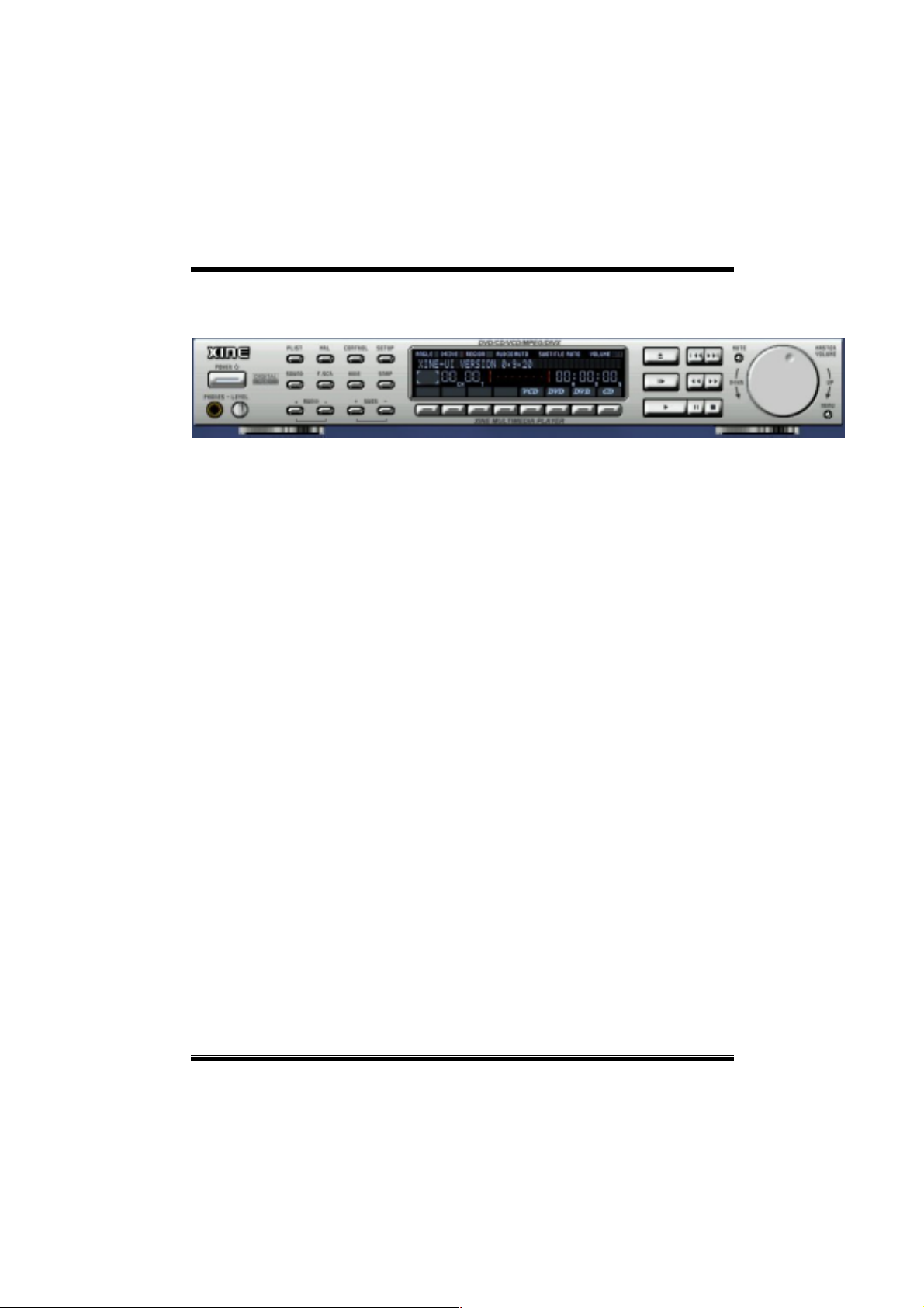
XINE
XINE is a multimedia player. It plays back Audio CD, DVD, and VCD. It also decodes
multimedi a fil es l i ke AV I, MOV, WMV, and MP 3 from l ocal disk drives. It interprets many of
the most common multimedia formats available - and some of the uncommon formats,
too.
• Features of Xine
a. Skinnable GUI
b. Navigation c ontrols (seeking, pause, fast, slow, next
chapter, etc)
c. On Screen Display (OSD) features
d. DVD and external subtitles
e. DVD/VCD menus (requires external plugin)
f. Audio and subtitle channel selection
g. Closed Caption support
h. Brightness, contrast, audio volume, hue, saturation
adjusting requires hardware/driver s up p ort)
i. Playlists
j. Image snapshot
k. Audio resampling
l. Software de-interlacing algorithms
m. Configuration dialog
n. Aspect ratio changing
o. Fullscreen display
• Supported File formats
a. Video CD
b. MPEG program streams (.mpg, .mpeg)
c. ogg (.ogg) avi (.avi)
d. asf (.asf, .wmv)
e. QuickTime (.mov)
30
Page 33

f. MPEG-Video (.mpv, .m2v)
g. MPEG-Audio (.mp2, .mp3)
h. WAV (.wav) Video Codecs
i. MPEG 1/2
j. MPEG 4 (aka OpenDivX)
k. MS MPE G 4
a. Chapter 5: Software Details 10
l. Windows Me dia Video 7
m. Motion JPEG
• Remote Control support.
a. Infrared interface
b. User-friendly
• Usage of StudioFun! with CelomaChrome skin
a. Select VCD button to play a VCD disc
b. Select DVD button to play a DVD disc
c. Select CDDA button to play a Audio cd
d. Select next chapter or MRL (>>|) button to play next track
in Audio CD, VCD and MP3 songs and to play next
chapter in DVD
e. Select previous chapter or MRL (|<<) button to play
previous track in Audio CD, VCD and MP3 song s an d to
play previous chapter in DVD
f. Select slow motion (<<) button to play the video / audio in
slow motion (Select play button after reaching the required
position)
g. Select fast motion (>>) button to play the video / audio in
fast motion (Select play button after reaching the required
position)
h. Select subs + / - button to select the appropriate subtitle
(Usable while playing
i. Select audio + / - button to select the appropriate audio
track (For example when
j. The DVD contains one audio track in English and the
other with some other language,
k. Usable while playing DVD’s)
31
Page 34

l. j. Select hide button to hide the control panel of the player
m. k. Select menu button to use menu’s while playing DVD
n. l. Select control button to adjust brightness / color
o. Select setup button to modify the settings of the player
p. Select f.scr button to show the video output of the player in
q. Select snap button to take a snapshot of the currently
r. Select plist button to add / remove / manage playlist
s. Select mrl button to add new file to play
Error Messages
full screen mode
playing video
The following error message is given if an unknown
file format is selected through Xine MRL browser
and played.
While playing mp3 files, if the user stops playing and
tries to select the DVD button, then the following
error message is shown
Select Region
Overview
Select region is a utility to set a DVD region. With the help of this application user can set
or change a DVD region. Only one region can be set at a time.
About Select Region
With the help of this application you can set a region for DVD. Only one region can be set
at a time. If you keep the mouse pointer on any region, y ou can view the countries, which
comes under that region.
Ok - Click to set the selected region.
Cancel - Click to quit the application.
How to select DVD region
You can select only one region at a time. You can change your selection by clicking on
any other region.
• A snapshot of the application is shown below:
32
Page 35

Screensaver
Screensaver
The xscreensaver da emo n w ait s un ti l the key boar d and mou se ha ve be en idl e for a peri od,
and then runs a graphics demo chosen at random. The demo is terminated as soon as
there is any mouse or keyboard activity.
The xscreensaver-demo program is the graphical user interface to xscreensaver. It lets
you tune the various parameters used by the xscreensaver daemon, and browse through
the graphics demos.
StudioFun! comes with xscreensaver when you click on the screensaver icon t he
application comes up. Then user can choose various graphics demos like
chbg,halo,hypercube or hyperball.
Screensaver comes with various options
• Preview Option: When a user selects a particular graphics demo and clicks on preview
button the demo comes up.
• Blank After Option: The screensaver will blank the screen after the keyboar d and mouse
have been idle default time is 1minute and user can change the settings.
• Cycle After Option: When screensaver is running this cycle time defines the time limit for
each screensaver.
• Mode Screensaver comes with various modes:
1. Random Screen Saver: When user chooses this option, Screensaver cycles through
various graphics demos randomly
33
Page 36
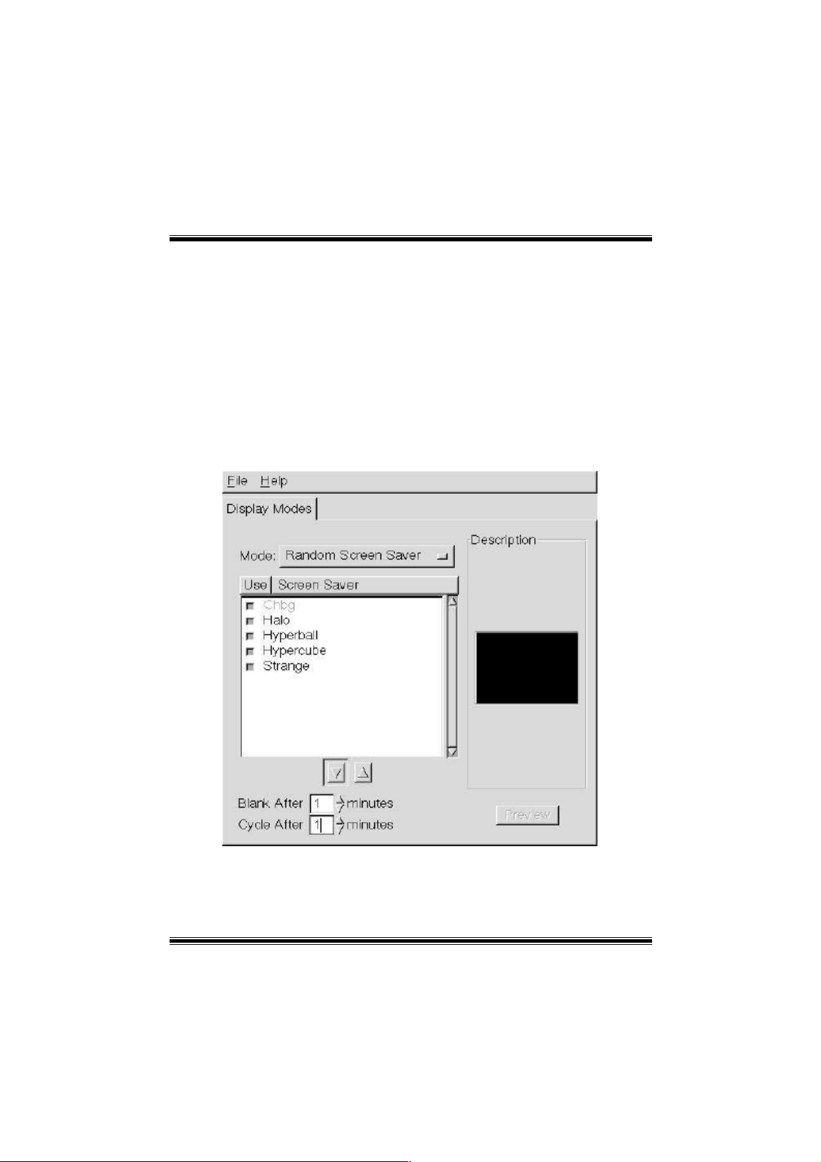
2. Only one Screen Saver: When user chooses this opti on, screensaver displays only one
graphics demo.
3. Blank Screen Onl y: When user chooses t his op ti on, scre e nsa ver onl y bl an ks the scr ee n
instead of displaying the graphics demo.
4. Disable Screen Saver: When user chooses this option, screensaver is disabled.
• Various Graphics Demos
XScreensaver comes with various screensaver
Chbg: This screensaver displays the images store d in StudioFun! the time gap between
images is 5 seconds.
Hyperball
Hypercube
Halo
Strange
• A snapshot of the application is shown below:
Display Settings
Display Settings
Display setting is a program to change the current resolution settings of the Display.
By default user of StudioFun will be given a choice to select between any of the following
34
Page 37

three resolutions.
• 640x480
• 800x600
• 1024x768
The current resolution of the Display will be selected by default. It requires restart of the
StudioFun to reflect the changes made.
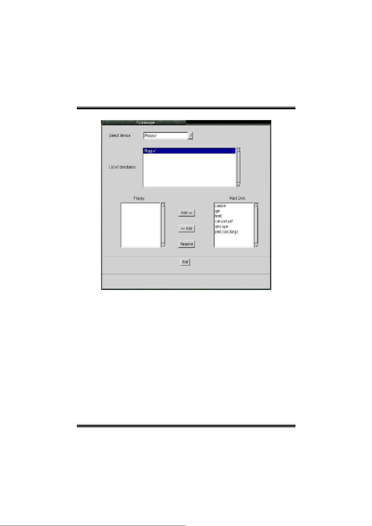
File Manager
Overview
File manger is an utility to copy files from deferent devices to hard disk and vice versa.
User can copy files from devices such as, floppy, cdrom and flashdisk to hard disk. And
also from hard disk to floppy and fl ashdisk.
About File manager
The hard disk files are stored in a directory called “/studiofun” on the hard disk. You can
also delete files from hard disk, but you cannot delete files from any device.
Select device - Contains the devi ce names /floppy, /cdrom and /flashdisk. Select a
device from/t o which y ou want t o copy fil es.
twice to m ou n t th e de vice .
List Directories - Shows the list of directories of the selected device after double
clicking it .
Floppy/cdrom/Fl a shdisk - Show s the contents of the selected direct ory from the “List
directories“ field after double clicking it.
Hard disk - Shows the contents of a directory called “/studiofun”.
Add (>>) - Click to copy selected files from a device to hard disk.
Add (<<) - Click to copy selected files from hard disk to a device.
Remove - Click to delete files from hard disk.
Exit - Click to quit the application.
Please doubl e cl ick the device option
35
Page 38
36
Page 39
Trouble Shooting
PROBABLE SOLUTION
No power to the system at all Power light don’t
illuminate, fan inside power supply does not turn
on. Indicator light on keyboard does not turn on
PROBABLE SOLUTION
System inoperative. Keyboard lights are on,
power indicator lights are lit, hard drive is
spinning.
PROBABLE SOLUTION
System does not bo ot from hard disk drive, can
be booted from CD-ROM drive.
PROBABLE SOLUTION
System only boots fr om CD- RO M. H ard di sk can
be read and applications can be used but
booting from hard disk is impossible.
* Make sure power cable is securely plugged in
* Replace cable
* Contact technical support
* Using even pressure on both ends of the
DIMM, press down firmly until the module
snaps into place.
* Check ca bl e r unning from disk to disk con tr oller
board. Make sure both ends are securely
plugged in; check the drive type in the
standard CMOS setup.
* Backing up the hard drive is extremely
important. All hard disks are capable of
breaking down at any time.
* Back up data and app li c ati ons file s. Reformat
the hard drive. Re-install ap plications and data
using backup disks.
PROBABLE SOLUTION
Screen message s ays “Invalid C onfiguratio n” or
“CMOS Failu re.”
PROBABLE SOLUTION
Cannot boot syst em af ter ins tallin g sec ond h ard
drive.
* Review system’s equipment . Make sure
correct inform ation is in setup.
* Set master/slave jumpers correctly.
* Run SETUP progra m and select correct drive
types. Call drive manufacturers for
compatibility with other drives.
37
Page 40
A
Problemlösung
MÖGLICHE URSACHE LÖSUNG
Das System hat keine Spannungsversorgung.
Die Stromanzeige leuchtet nicht, der Lüfter im
Inneren der Stromversorgung wird nicht
eingeschaltet. Tastaturleuchten sind nicht an.
MÖGLICHE URSACHE LÖSUNG
Das System funktioniert nicht. Die
Tastaturleuchten sind an, die Stromanzeige
leuchtet, die Festplatte dreht sich.
MÖGLICHE URSACHE LÖSUNG
Das System wird von der Festplatte nicht
hochgefahren, vom CD-ROM-Treiber aber ja.
MÖGLICHE URSACHE LÖSUNG
Das System wird nur von der CD-ROM
hochgefahren. Die Festplatte wird gelese n und
die Anwendungen sind funktionsfähig, aber es
ist nicht möglich, das System von der Festplatte
zu starten.
uf dem Bildschirm erscheint die Meldung
“Ungültige Konfiguration” oder “CMOS Fehler.”
Das System kann nach der Installation einer
zweiten Festplatte nicht hochgefahren werden.
MÖGLICHE URSACHE LÖSUNG
MÖGLICHE URSACHE LÖSUNG
* Versichern Sie sich, dass das Stromkabelrichtig
angebracht ist
* Ersetzen Sie das Stromkabel
* Wenden Sie sich an Ihre Kundendienststelle
* Drücken Sie das DIMM-Modul bei gleichem
Druck an beide Seiten, bis es einrast et.
* Überprüfen Sie das Kabel zwischen Festplatte
und Festplatten-Controller. Versichern Sie
sich, dass beide Enden richtig angebracht
sind; überprüfen Sie den Laufwerktyp in der
standardmäßigen CMOS-Einrichtung.
* Ein Backup der Fes tplatte i st sehr wi chtig. Alle
Festplatten können irgendwann beschädigt
werden.
* Machen Sie eine Sicherungskopie von allen
Daten und Anwendungsdat eien. Formatieren
Sie die Festplatte und reinstallieren Sie die
Anwendungen und Daten mit Hilfe von
Backup-Disks.
* Überprüfen Sie die Systemkomponenten und
versichern Sie sich, das diese richtig
eingerichtet sind.
* Setzen Sie die Master/Slave-Jumper richtig ein.
* Führen Sie das SETUP-Programm aus und
wählen Sie die richtigen Laufwerktypen.
Wenden Sie sich an den Lau fwerkhersteller,
um die Kompati bilität mit an deren Lauf werk en
zu überprüfen.
38
Page 41

05/21/2003
39
 Loading...