

Changhong LT26GJ01E, LS01+DVB-T Schematic

LCD COLOUR TV
SERVICE MANUAL
CHASSIS NO.: LS01+DVB-T
Please read this manual carefully before service.
1

Catalog
Chapter 1: Specifications and Composition...................................................................3
Chapter 2: Function Introduction of Main IC ..................................................................8
Chapter 3: Analysis of Signal process Flowchart and key point measure date31
Chapter 4: Maintenance Procedure and Examples of Typical troubleshooting..42
Chapter 5: Spare Part Lists................................................................................................43
Chapter 6: Factory Setup and notice..............................................................................44
Appendix: 1. Circuit Schematic diagram
2. Circuit Schematic diagram of DVB module
3. Circuit Schematic diagram of power module
4. Final Assembly diagram
5. Wiring diagram of LCD TV with LS01 chassis (take
LT32GJ01E as an example)
2
Chapter 1: Specifications and Composition
1. Models for LS01 chassis :
Region Europe Asia
LT26GJ01EB LT32GJ01EB LT37GJ01EB LT26GJ12EB
LT32GJ12EB LT37GJ12EB LT26GJ88EB LT32GJ88EB
Original
Models
LT37GJ88EB LT26GJ01EBS LT32GJ01EBS LT37GJ01EBS
LT26GJ12EBS LT32GJ12EBS LT37GJ12EBS LT26GJ88EBS
LT32GJ88EBS LT37GJ88EBS
2. Main Feature
Region Europe America Other regions
Color
RF signal
Video or Y/C signal PAL、NTSC、SECAM PAL、NTSC、SECAM PAL、NTSC、SECAM
Program presetting 100 (0-99)
Audio output(THD≤7%) 5W+5W 5W+5W 5W+5W
Power source 100V~240V 100V~240V 100V~240V
Teletext 100 pages X 100 pages
CCD X Yes X
Sound demodulator NICAM、IGR BTSC NICAM、IGR
SCART Yes X X
VGA Yes Yes Yes
YPb P r Yes Yes Yes
HDM I Yes Yes Yes
Ear p h one Yes Yes Yes
OSD language
Auto Off without Signal
Reception
Program booking 5 program booking. Turn to the corresponding program at the booking time.
Swap Customer could rearrange the channels according to personal habit
Energy saving system Customer could adjust LCD screen backlight brightness manually to save energy.
Plug and Play
system
Sound
system
PAL 、SECAM NTSC、PAL M 、PA L N PAL 、NTSC、SECAM
D/K、B/G、I、L/L’ M D/K、B/G、I、M
68 (AIR:2-69)
125 CABLE:1-125)
English, French, German,
Italian, Portuguese etc.
5 minutes
LCD TV could be used as computer screen, no need for the installation of software,
which is Plug and Play in real sense
English, French,
Portuguese, Spanish etc.
3. Unit IC Compositions:
LT26GJ01AUB LT32GJ01AUB
LT37GJ01AUB LT42GJ01AUB
LT32GJ12AUB LT37GJ12AUB
LT26GJ88AUB LT32GJ88AUB
LT37GJ88AUB
236 (0-235)
English, French, German,
Spanish etc.
LCD TV with LS01 chassis is made up of switch power, system control circuit, video processing
circuit, audio processing circuit, Power Amplifier circuit, AV input circuit, LCD screen module. Block
circuit diagram is shown as below:
3
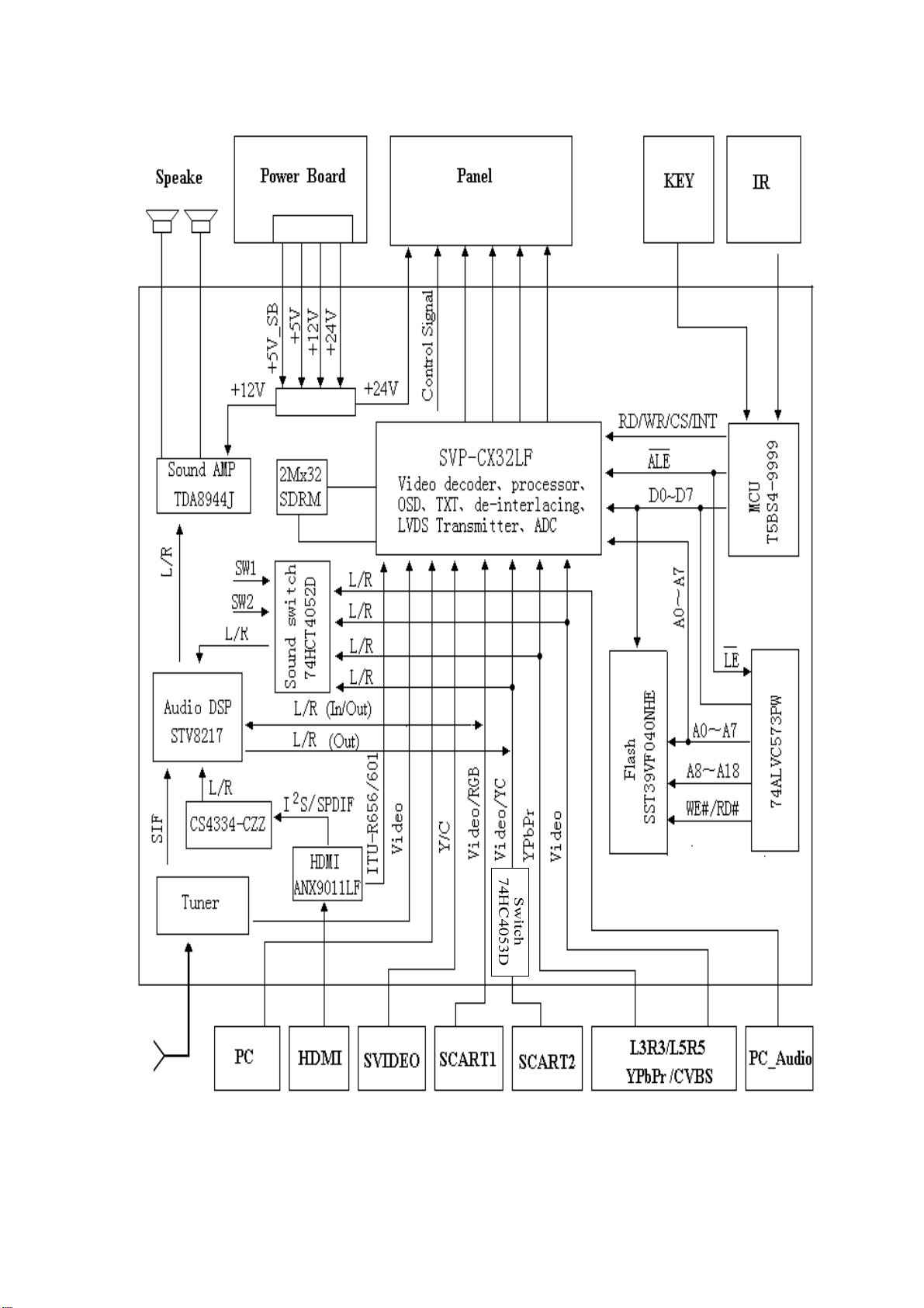
1) European market:
4
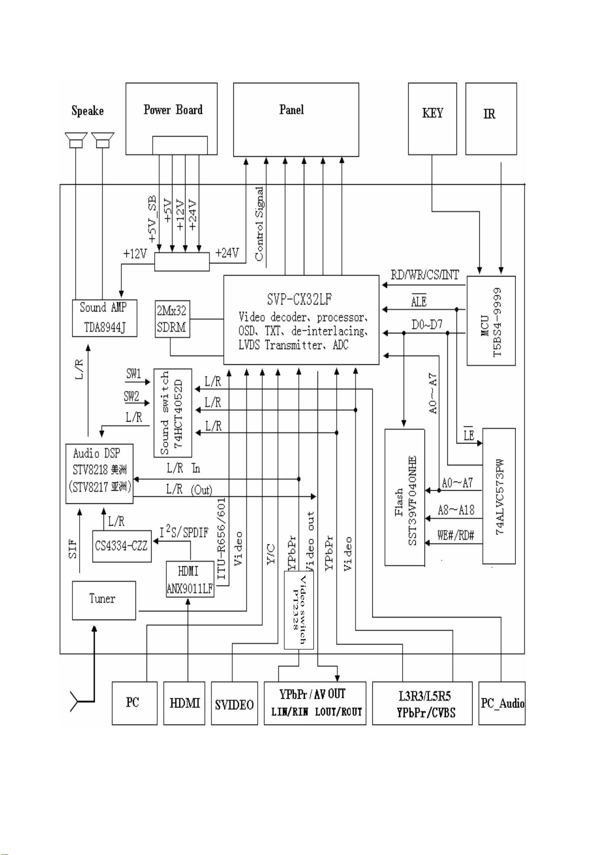
2). American and Asian market:
5
3) DVB Module
f
DVB-T TUNER
FLASH
DDR
RS232 Update
RS232 I/O
MPEG Decoder
STI7710
XILLEON225
Y
Pb Pr L R
Power
RCA
音频放
音频放
大
大
RCA
4. Introduction of PCB module
LCD TV with LS01 is made up of power board, side AV board, remote control reception board, key
board, and mainboard. The table below is the introduction of the function of all printed board modules.
No. Parts Description
Mainboard module is the core of LCD TV signal processing. Under the control o
the system control circuit, It undertakes the task of converting the external input
signal into the unified digital signal that the LCD screen could identify. Mainboard
controls the whole machine through IIC bus, decode VIDEO signal, controls the
Mainboard
1
module
Video (brightness, contrast, chroma, hue, definition etc), white balance adjusts,
generates OSD, de-interlaces signal, converts signal frequency, and finishes
signal A/D and D/A conversion, video enhancement, LVDS signal coding and
output; it has Scart , S-Video, AV , YPbPr, HDMI and PC interface, Tuner input,
sound demodulation, sound processing, sound power amplifier, and online
update.
6
Remote
r
2
reception
module
Built-in powe
3
board module
The remote reception board module is constituted by an indicator-light and a
remote reception. Customer could manipulate the LCD TV by using remote
controller very conveniently. By the color of the indicator light, the operation
mode of the LCD TV could be judged (red is standby, green is power on).
Convert the 100V~240V (50/60HZ)AC into DC, output have +24v, +12V, +5V,
and the +5V_STB in standby state.
Keyboard
4
module
LCD screen
5
module
Keyboard module has 7 function keys (program +/-, volume +/-, AV/TV,
menu ,power), customer could use the key to operate the TV freely.
LCD screen has built-in inverter that convert DC into high voltage AC signal to
turn on the backlight CCFL (Cold Cathode Fluorescent Light); the LCD screen
process the video signal from signal board and reappear.
6 Side AV board Side AV board is used for earphone output.
7
Chapter 2: Function Introduction of Main IC
1. Main ICs and functional modules of LS01 chassis
No. Item no. Model Main function
1 J11 JS-6G1/111A25-A2 Tuner output sound IF and video signal
2 U1 SVP-CX32LF
3 U2 IS42S32200C1-6TL SDRAM with 2MX32bits
4 U3 AT24C64A-10PU-2.7 EEPROM
5 U4 T5BS4-9999 MCU
6 U5 SST39VF040-70-4C-NHE Flash, Store the Control program.
7 U6 74ALVC573PW Address latch, to latch the address wires
8 U8 TCM809SENB713 Hardware reset IC of MCU
9 U9 74HCT4052D Audio input switch of AV terminal
10 U35 STV-8217/STV-8218 Audio signal processor
11 U14 74LVC14AD
12
14
U16、U25
U18、U22
AT24C02BN-10SU-1.8 EEPROM
AZ1117H -1.8TRE1 3.3V to 1.8V DC conversion
Video decoder, image processor, A/D and D/A
conversion
VGA line and field synchronizing signal waveform
shaping
16
18 U20 AZ1084S -3.3TRE1 5V to 3.3V DC conversion
19 U21 AZ1084S -1.8TRE1 5V to 1.8V DC conversion
20 U23 AZ78L08ZTR-E1 12V to 8V DC conversion
21 U26 CS4344-CZZ HDMI digital audio decode, DAC
22
24 U30 ANX9011L HDMI digital signal decode
25 U31 PI5C3306LE (SDA, SCL) used for program update
26 U33 TDA8944J Audio amplifier (BTL output)
27 U37 74HC4053D Audio input switch
28 U38 PT2328 Video input switch
U19、U24
U28、U29
AZ1117H -3.3TRE1 5V to 3.3V DC conversion
Rclamp0514M.TBT ESD protection device of HDMI
8
2. Function introduction of ICs or functional module of LCD TV with
LS01chassis
1.Tuner (J S -6 G1 /111 A25-A2 )
Pin No. Definition of pin Function description
1 VCC +5V power
2 BT No connection
3 VCC +5V power
4 SCL IIC bus (clock)
5 SDA IIC bus (data)
6 AS Ground
7 AFS Ground
8 NC No connection
9 NC No connection
10 NC No connection
11 SIF/Out Sound intermediate Frequency output
12 Video/Out CVBS signal output
13
14 Audio/Out Audio signal output
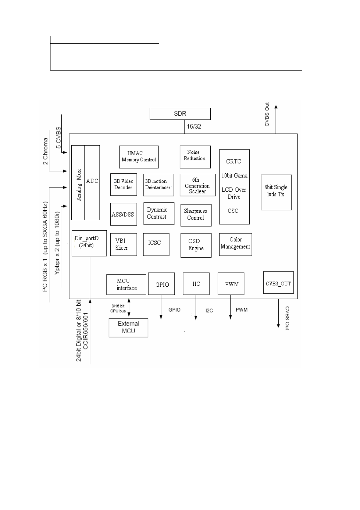
2. Image processing IC SVP-CX32LF
The SVPTMCX video processor is a highly integrated system-on-a-chip device, targeting the
converging HDTV ready and PC-ready LCD TV, PDP TV applications where high precision
processing of video and data are the requirements. SVPTMCX contains 6th generation
dual-purposed triple 10-bit high-precision and high speed video ADCs for both PC and video inputs,
the high-performance multi-format 3D digital comb video decoder that supports NTSC, PAL, and
SECAM*, a HDTV sync separator, motion adaptive de-interlacing engine, and the video format
conversion engine, supporting multi-window display in many different output modes. Trident’s
DCReTM – Digital Cinema Reality engine, is integrated inside the SVPTMCX family to provide the
most natural cinema-realistic images. The DCReTM technology integrates advanced 3D-comb video
decoding, advanced motion adaptive de-interlacing, object-based digital noise reduction, advanced
6th generation scaler, film mode support, average picture level (APL), edge smoothing and dynamic
sharpness enhancement. Trident's patented Unified Memory Architecture (UMA) that allows frame
rate conversion, 3D comb video decoding, and video enhancement processing to share the same
memory buffer that is made up of high-speed and cost-effective PC graphic memory. All these
advanced digital processing techniques combined with a true 10-bit video data processing for the
most optimal video fidelity to provide the most natural and cinema quality video images. Designed for
maximum system design flexibility, SVPTMCX integrates all video interfaces to support converging
digital video, analog video, and PC data applications. The users of Trident's single chip SVP™CX
series video processor(s) will benefit from many features while maintaining a price competitive
advantage over the existing solution(s)
Main features:
●Integrated 6th Generation Motion and Edge Adaptive De-interlacing
● Integrated ADC
● PC auto tune
●Built-in 8-bit LVDS Transmitter
● 6th generation cubic-4 image scaling engine
● Advanced Chroma Processing and Dynamic Contrast Function
● Green color stretch, blue color stretch, skin color enhancement
●Integrated 6th Generation Motion Adaptive 3D Digital Comb Video Decoder with
Programmable Filter
●60Hz~100Hz interlaced scanning and 50Hz~75Hz progressive scanning
● Frame rate conversion
● 14D: dynamic picture enhancements
● Advanced Film Mode Recovery-3:2/2:2 pull down
● Build-in A/D conversion function
● Teletext function
VCC(+5V)
+5V power
9
● Supports 16/32bits SDRAM memory interface
● Multi-screen display mode
● OSD and VBI/Closed caption and advanced OSD engine
Pin function description:
Pin No. Designation of pin Function of pin
Analog signal input/output terminal
169 CVBS1 CVBS input 1
180 Y_G1 Y input
181 Y_G2 SCART1 Green signal input
182 Y_G3 S-Video Y signal input
183 PC_G PC Green signal input
188 PR_R1 DVD interface Pr signal input
189 PR_R2 SCART1 Red signal input
190 PR_R3 SCART2 Y signal input
191 PC_R PC Red signal input
192 C S-Video C signal input
196 PB_B1 DVD interface Pb signal input
197 PB_B2 SCART1 Blue signal input
198 PB_B3 SCART1 CVBS signal input
199 PC_B PC blue signal input
171 FS1 No connection
170 FS2 No connection
173 FB1 SCART1 RGB_FB signal input
172 FB2 SCART2 chroma signal input
174 VREFP_1 A/D conversion1 voltage reference +
175 VREFN_1 A/D conversion 1 voltage reference 184 VREFP_2 A/D conversion 2 voltage reference +
185 VREFN_1 A/D conversion 2 voltage reference -
Digital signal terminal
37 DP0
┆ ┆
29 DP8
26 DP9
25 DP10
24 DP11
22 DP12
21 DP13
Digital signal I/O(DP0~DP23)interface
18 DP14
┆ ┆
14 DP18
11 DP19
┆ ┆
7 DP23
CPU control terminal
55 PWMO Pulse width modulation input
57 SCL
58 SDA
IIC(clock)
IIC(data)
60 GPIO0 GPIO1 selection signal
59 GPIO1 GPIO2 selection signal
62 WR# CPU write signal
63 RD# CPU read signal
61 CS
56 INTN
CPU chip selection signal(low level effective)
Interrupt signal(low level effective)
84 ALE Address latch signal
86 RESET Reset signal (high level effective)
85 V5SF
SF Power(+5V)
4 DP_HS Line synchronization signal
10
5 DP_VS Field synchronization signal
23 DP_CLK Digital port Clock
6 DP_DE_FLD DE I/O terminal
64 ADDR0
┆ ┆
CPU address(R0~R7)signal
71 ADDR7
83 A_D0
┆ ┆
CPU address/data passage
76 A_D7
MISC port control signal
162 CVBS_OUT2 SCART2 interface CVBS signal output
163 CVBS_OUT1 SCART1 interface CVBS signal output
157 TEST MODE Test mode signal (grounding)
158 AIN_HS Line synchronization signal
159 AIN_VS Field synchronization signal
205 XTALI
204 XTALO
Crystal oscillator interface
SDRM controlling port
124 MA0
┆ ┆
121 MA3
118 MA4
┆ ┆
Memory address (A0~A11)
113 MA9
125 MA10
126 MA11
156 DQM0
133 DQM1
109 DQM2
Memory read/write byte signal
87 DQM3
128 BA0
127 BA1
Memory stack address selection
130 RAS# RAS signal
131 CAS# CAS signal
132 WE# Memory write pulse
112 CLKE Memory clock pulse
129 CS0# Memory chip selection signal
111 MCK Memory clock signal
155 MD0
┆ ┆
148 MD7
145 MD8
┆ ┆
138 MD15
107 MD16
Memory data interface
┆ ┆
100 MD23
95 MD24
┆ ┆
88 MD31
LVDS port
52 LVDS_VDDP Power for LVDS
38 PLL_GND PLL ground
39 PLL_VCC PLL power
47 LVDSGND LVDS ground
46 LVDSVCC Power for LVDS
43 TCLK1M Positive/Negative LVDS differential clock output
11
42 TCLK1P
51 TA1 M
50 TA1P
49 TB1M
48 TB1P
45 TC1M
Positive/Negative LVDS differential data output
44 TC1P
41 TD1M
40 TD1P
Clock and power
146 VDDM
134 VDDM
108 VDDM
Memory port digital power
98 VDDM
72 VDDH
19 VDDH
3.3V power supply
160 VDDC
136 VDDC
119 VDDC
96 VDDC
74 VDDC
1.8V power supply
53 VDDC
27 VDDC
12 VDDC
13 VSSC
28 VSSC
54 VSSC
75 VSSC
97 VSSC
120 VSSC
137 VSSC
161 VSSC
Digital ground
20 VSSH
73 VSSH
99 VSSM
110 VSSM
135 VSSM
147 VSSM
195 AVDD3_ADC2
168 AVDD3_ADC1
ADC analog power (+3.3V)
2 PLF2 Video PLL clock low pass filtering
207 MLF1 Memory PLL clock low pass filtering
1 PAVSS2 PLL ground
3 PAVDD2 PLL power (+1.8V)
206 PAVSS1 PLL digital ground
208 PAVDD1 PLL digital ground power (+1.8V)
203 PAVSS PLL Digital ground
202 PAVDD PLL digital ground power(+1.8V)
201 PDVSS PLL Digital ground
200 PDVDD PLL digital ground power (+1.8V)
177 AVDD_ADC1
186 AVDD_ADC2
193 AVDD_ADC3
ADC analog power (+1.8V)
178 AVDD_ADC4
176 AVSS_ADC1
187 AVSS_ADC2
194 AVSS_ADC3
ADC analog ground
179 AVSS_ADC4
12
165 AVDD3_OUTBUF
164 AVSS_OUTBUF
166 AVDD3_BG_ASS
167 AVSS_BG_ASS
SVP-CX32LF internal block diagram:
+3.3V analog power
Analog ground
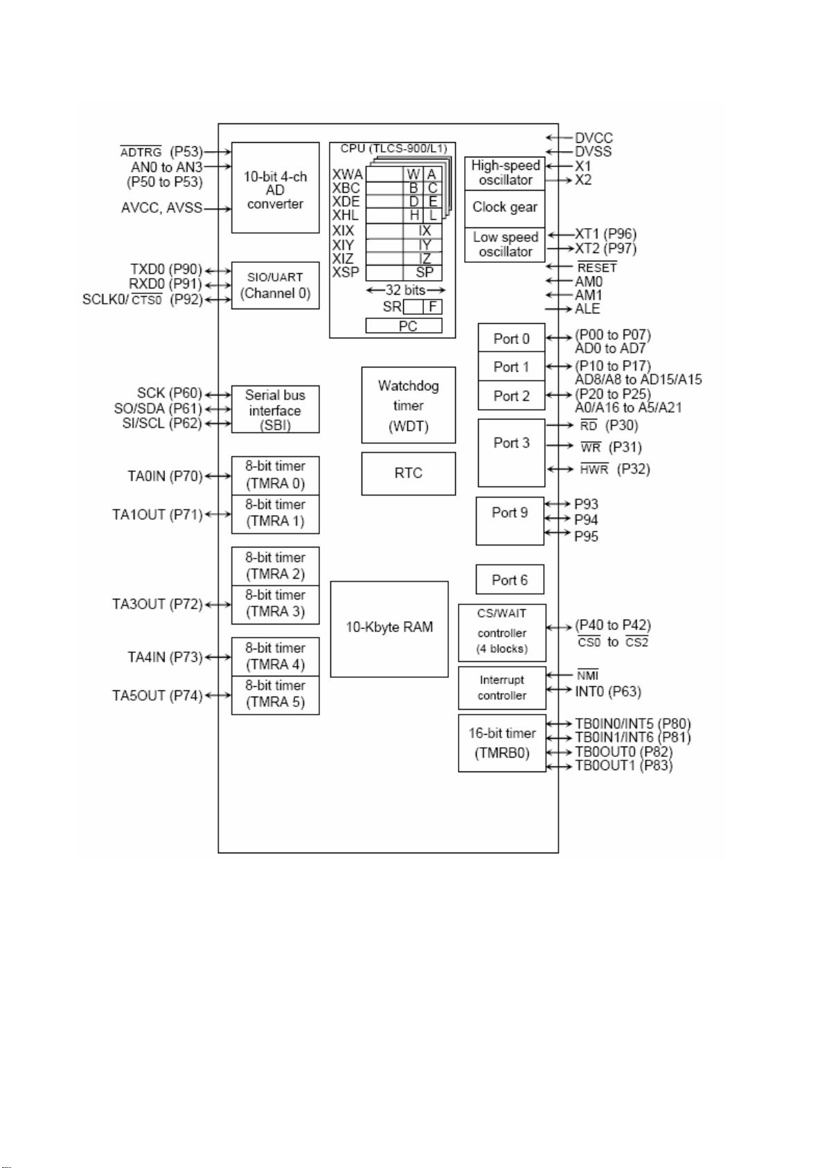
3.T5BS4-9999 brief introduction:
T5BS4-9999 is a high-speed 16-bit micro-controller designed for the control of various mid- to
large-scale equipment. T5BS4-9999 is ROM-less product, T5BS4-9999 comes in a 64-pin flat
package. Listed below are the features that is used for the control of a variety of small to large
devices. T5BS4-9999 could extend ROM ,64 pins and is packaged in PLCC. It is the main control
IC of the TV via I²C bus.
Main features:
●High speed 16-bit CPU(900/L1 CPU)
● Minimum instruction execution time: 148ns
● Build-in RAM: 10Kbytes
● Expandable up to 16Mbytes
● simultaneously support 8-/16-bit width external data bus
● 8-bit timers: 6 channels, 16-bit timers: 1 channel
13
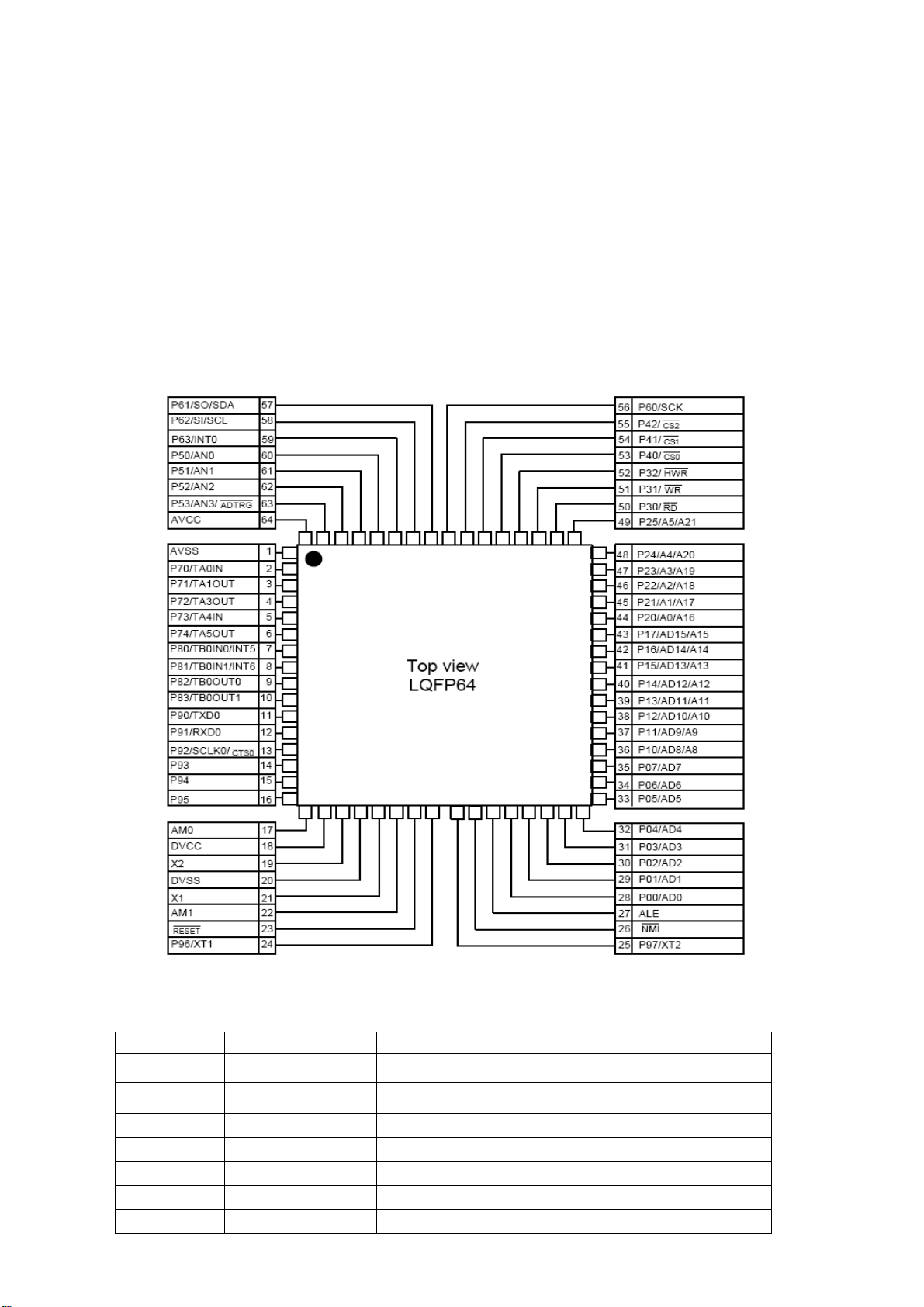
●General-purpose serial interface: 1 channel
●Serial bus interface: 1 channel
●10 bit A/D conversion interface: 4 channels
●Watchdog timer
● Timer for real time clock (RTC)
● Chip select/wait controller: 4 blocks
● 34 interrupt signals output
9 CPU interrupt, 21 internal interrupt, 4 external interrupt
● 53 I/O pins
● Standby function
● Clock control
fs=32.768KHz real-time time of time conversion function high frequency fc to fc/16
● Working voltage
When fc=27 MHZ, VCC=2.7~3.6V, when fc=10MHZ, VCC=1.8V to 3.6V
● 64 pin package(P-LQFP64-1010-0.50D standard)
Pin assignment description:
Pin introduction:
Pin
1
2
3
4
5
6
7
Designation Function description
AVSS Analog ground
P70/TA0IN
P71/TA1OUT
I²C data input
I²C clock output
P72/TA3OUT PAGE signal output
P73/TA4IN +5V power
P74/TA5OUT Backlight on/off control
P80/TB0IN0/INT5 Remote control signal
14
8
9
10
11
12
13
14
15
16
17
18
19
20
21
22
P81/TB0IN1/INT6 +1.8V power supply
P82/TB0OUT0 Remote red control signal
P83/TB0OUT1 Remote green control signal
P90/TXD0 Digital ground
P91/RXD0 HDMI identity signal
P92/SCLK0/
P93 CON4(10
P94 CON4(4
P95 CON4(3
AM0 Bus byte selection
DVCC +3.3V power
X2 Crystal oscillator interface
DVSS Ground
X1 Crystal oscillator interface
AM1 Bus byte selection
23
24
25
26
27
28
┆
35
36
┆
43
44
┆
49
50
51
52
P96/XT1 Low frequency oscillation input interface
P97/XT2 Low frequency oscillation output interface
NMI Interrupt request signal
ALE Address latch pulse
P00/AD0
┆
P07/AD7
P10/AD8/A8
┆
P17/AD15/A15
P20/A0/A16
┆
P25/A5/A21
P30/
P31/
P32/
53 P40/
54
P41/
55 P42/
56
57
58
59
60
61
62
63
64
P60/SCK (no connection)
P61/SO/SDA
P62/SI/SCL
P63/INT0 Interrupt request signal
P50/AN0
P51/AN1
P52/AN2 SCART1 FS signal
P53/AN3/
AVCC
No connection
th
pin)
th
pin)
rd
pin)
CPU reset control port
0~7 bit address/data port
8~15 bit address/data port
or 8~15 bit address port
8~5 bit address port
or 8~21 bit address port
External memory read control terminal
External memory write control terminal (AD0~AD7)
Data write control terminal (AD8~AD15)
Internal address selection signal
I²C data
I²C clock
KEY signal port
SCART2 FS signal
Analog power (+3.3V)
15
T5BS4-9999 internal functional block diagram:
4.STV-8217/STV-8218 brief introduction
STV-8217/STV-8218 main features:
■ Full-Automatic Multi-Standard Demodulation
● B / G / I / L / D / K / M / N Standards
● Mono AM and FM
● FM 2-Carrier and NICAM/BTSC
■ Sound Processing: Loudspeaker
● ST royalty-free processing: ST WideSurround, ST
OmniSurround (Virtual Dolby
ٛ Surround and
● Independent Volume / Balance
16
● Smart Volume Control (SVC), 5-band equalizer and Loudness
■ Analog Audio Matrix
● 4 stereo inputs
● 3 stereo outputs
● THRU mode
● 2 VRMS capability
Pin introduction:
Pin
1
2
3
4
5
6
7
8
9
10
11
12
13
14
15
16
17
18
19
20
21
22
23
24
25
26
27
28
29
30
31
Designation Function description
SC1_OUT_L SCART1 audio output left
SC1_OUT_R SCART1 audio output right
VCC_H +8V power
GND_H ground
SC3_OUT_L SCART3 audio output left
SC3_OUT_R SCART3 audio output right
VCC33_SC +3.3V power
GND33_SC Ground
SC1_IN_L SCART1 audio output left
SC1_IN_R SCART1 audio output right
VREFA Audio bias voltage decoupling interface
GND_SA Ground
VBG Audio bias voltage decoupling interface
SC2_IN_L SCART2 audio input left
SC2_IN_R SCART2 audio input right
VCC33_LS DACs power(+3.3V)
GND33_LS DACs ground
SC2_OUT_L SCART2 audio output left
SC2_OUT_R SCART2 audio output right
VCC_NISO
GND_SA
Polarization of the NISO(+3.3V)
DACS ground
VSS33_CONV DAC ground
VDD33_CONV DAC power (+3.3V)
SC3_IN_L SCART3 audio input left
SC3_IN_R SCART3 audio input right
SCL_FLT SCART channel filtering left
SCR_FLT SCART channel filtering right
LS_C No connection
LS_L Left loudspeaker output
LS_R Right ludspeaker output
LS_SUB No connection
HP_LSS_L No connection
17
32
33
34
35
36
37
38
39
40
41
42
43
44
45
46
47
48
49
50
51
52
53
54
55
56
57
58
59
60
61
62
63
64
65
66
67
68
69
HP_LSS_R No connection
VSS18_CONV DAC/ADC ground
VDD18_CONV DAC/ADC power (8V)
/HP_DET Earphone detection
ADR_SEL hardware address selection for IIC bus
VSS18 Digital ground
VDD18 +1.8V power
SCL I²C bus clock
SDA I²C bus data
VSS18 Digital ground
VDD18 +1.8V power
/RST Reset signal input/output terminal
S/PDIF_IN No connection
S/PDIF_OUT No connection
VDD33_IO1 +3.3V power
VSS33_IO1 Digital ground
CK_TST_CTRL Digital ground
VSS18 Digital ground
VDD18 +1.8V Power
CLK_SEL Clock input format selection
XTALIN_CLKXTP
XTALOUT_CLKXTM
Oscillator interface
VCC18_CLK1 1.8V for clock PLL
GND18_CLK1 Ground
GND18_CLK2 Ground
VCC18_CLK2 +1.8V Power
VSS33_IO2 Digital ground
VDD33_IO2 +3.3V Power
I2S_PCM_CLK No connection
I2S_SCLK I²S clock I/O channel1,2,3
I2S_LR_CLK I²S selection signal input/output
I2S_DATA0 I²S bus data input/output stereo channel 1
I2S_DATA1 I²S bus data input stereo channel 2
I2S_DATA2 I²S bus data input stereo channel 3
VDD18 +1.8V Power
VSS18 Ground
BUS_EXP Bus-expander function
IRQ No connection
18
70
71
72
73
74
75
76
77
78
79
80
GND_PSUB Ground
VDD18_ADC +1.8V Power
VSS18_ADC Ground
SIF_P Sound IF input (positive terminal)
SIF_N Sound IF input (negative terminal)
GNDPW_IF Ground
VCC18_IF +1.8V Power
GND18_IF Ground
MONO_IN Mono input
SC4_IN_L SCART4 audio input left
SC4_IN_R SCART4 audio input right
STV-8217 internal block diagram:
19
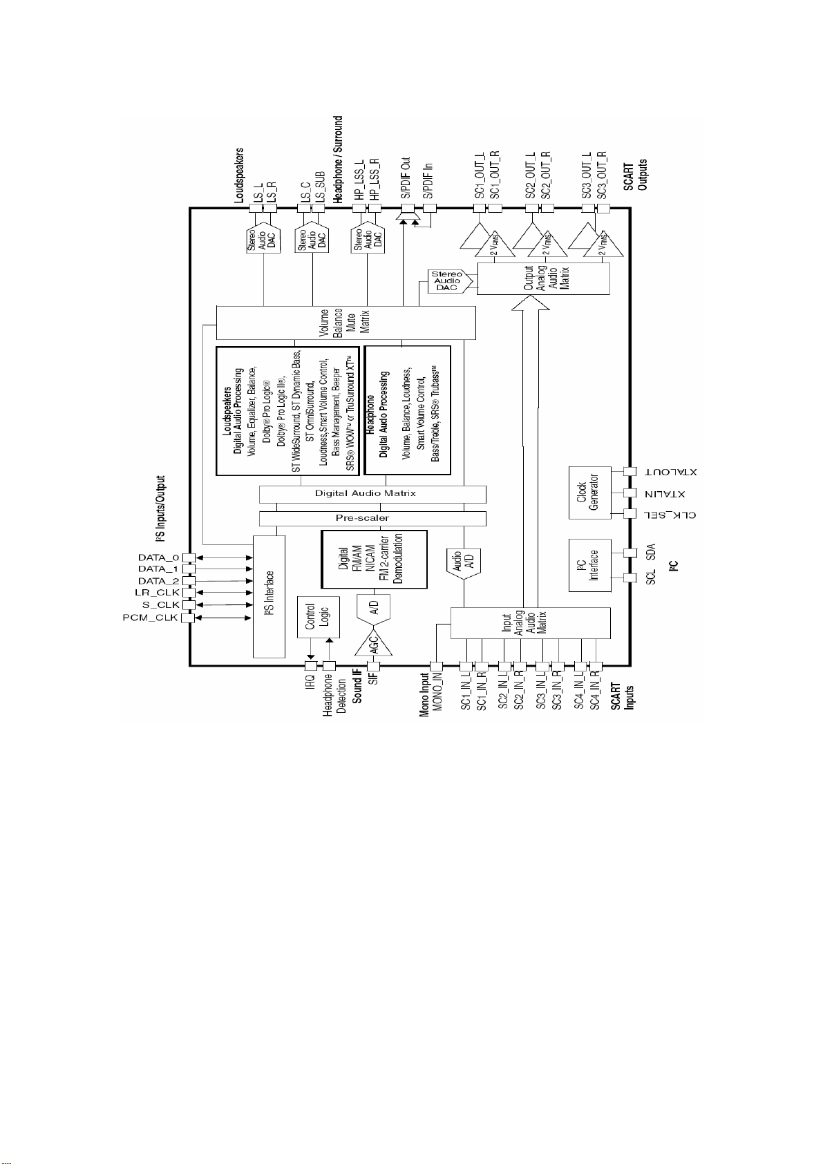
STV-8218 internal block diagram:
20
 Loading...