

Page 1

LCD/PDP TV
MODEL: LS0B CHASSIS
SERVICE MANUAL
(18.5 inches LED TV as an example,General version)
Please read this manual carefully before service.
Page 2

CATALOG
Chapter1:Safety and notes..........................................................................................3
1.1 Installation notes .................................................................................................................3
1.2 Attention points of operation and using ..............................................................................3
1.3 Storage notes.......................................................................................................................3
1.4 Dismantling notes ...............................................................................................................3
1.5 High-voltage warning .........................................................................................................3
Chapter2: Whole machine standard and terminal functions..................................4
2.1 Basic standard .....................................................................................................................4
2.2 Introduction of terminals(practicality photos).....................................................................5
Chapter3:Main chip functions and brief introductions of power supply...............6
3.1 MAIN IC and functions of LS0B........................................................................................6
3.2 Pin function description of LS0B chip................................................................................6
3.3 Brief introduction of power supply...................................................................................10
Chapter4: The chassis frame diagram, mainboard power supply systems,
mainboard interface definition and the waveform of key points .......................... 11
4.1 The chassis frame diagram................................................................................................ 11
4.2 Power supply system.........................................................................................................11
4.3 The waveform of key points .............................................................................................13
Chapter5: Software upgrade tooling,software upgrade instructions,software
initialization,parameter setting,software version and screen matching
instructions................................................................................................................. 14
5.1 Software upgrade tooling ..................................................................................................14
5.2 Software upgrade instructions...........................................................................................14
5.3 Software initialization .......................................................................................................18
5.4 Software version ...............................................................................................................19
Chapter6:Classical accident maintenance procedures and examples...................20
6.1 Clues of can’t boot ............................................................................................................20
6.2 Common problems for your reference:.............................................................................22
Chapter7: Spare Part Lists.......................................................................................23
Chapter8: Factory mode parameter setting instructions and notes.........................24
8.1 Enter into the factory mode...............................................................................................24
8.2 Setting method of factory menu........................................................................................26
Chapter9:Instructions of simple factory debugging specification.........................27
9.1 Clear EEPROM ,and set the parameters after upgrading according to the upgrade
instructions..............................................................................................................................27
9.2 Check each channel/source to see if the image and sound are normal..............................27
2
Page 3

Chapter 1: Safety and notes
1.1 Installation notes
(1) Please don't beat or rub, scratch the surface of the LCD screen heavily, don’t touch it with
hand casually.
(2) When the screen is dirty, please clean it with absorbent cotton or cotton cloths lightly.
(3) Please clean the screen timely when water or other viscosity pollution falls on it, which may
make the LCD face or color changes.
(4) Please don’t make the LCD screen shocked by a strong external force.
1.2 Points of operation and using for attention
(1) Please unplug the power cable before moving LCD screen.
(2) Please don’t change the mainboard’s original setting; otherwise brightness, white balance etc.
may not meet the specification.
(3)The amount of radiation of long time use at room temperature is larger than that at low
temperature.
(4) Please note that the long displaying image may remain at the top when shutdown the
machine.
(5) Please avoid the impact from mobile phone to protect your TV.
1.3 Storage notes
(1)When store for a long time, please keep the temperature between 0℃to 40℃, don’t expose the
TV to the sun , the humidity should be less than 85%RH.
(2)Please don’t put your TV under high humidity and high temperature circumstance, e.g.
temperature: 60℃, humidity:85%RH.
(3)Please don’t put your TV under low temperature circumstance, e.g. temperature lower than
25℃.
1.4 Dismantling notes
(1) As LCD screen can be damaged easily when dismantle, please pay attention to protect it.
(2)Please pay attention to the position of each screw when dismantle in case of beating the wrong
position when install which may lead to crack or slide of the face frame.
(3) If you need to dismantle the power board or the main board, please attention the position and
direction of each line, especially the direction of the screen line, in case of causing accident
when install. Before dismantle, we can take some photos of the line routes for the comparison
of installing.
(4)After check and maintenance, please assure that there is no foreign body in the machine when
install.
1.5 High-voltage warning
The high-voltage of the LCD screen is generated by the power supply step-up board, without
attention to exposure to high voltage; one may meet a serious electric shock.
3
Page 4

Chapter2: Whole machine standard and terminal functions
2.1 Basic standard
item standard
visual area 18.5 inches(diagonal) (CPT)
aspect ratio 16:9
resolving ratio 1366 x768
visual area H x V 409.8m m (H) ×230.4m m (V)
display color 16.7 million
LCD Panel
contrast 1000:1
brightness 250cd/m2
visual angle 170°(horizontal)/ 160° (vertical)
response time 5ms
backlight life 25000 hours
the parameters are
for reference only,
the specification
should accord to
the standard of the
panel of the batch
orders
TV function
audio and video
signal input
Video output
Audio
Power
Panel rotation
sound system B/G、D/K、I、M
color system PAL / SECAM / NTSC
AV RCA x 1 Audio L/R x 1
COMPONENT YPbPr x 1
HDMI HDMI x1 support to1080P
plug and use USB2.0
PC input
input frequency
recommend 1024x768(60HZ)
Output CVBS signal
Audio output L / R
power supply AC100V~240V, 50/60Hz
power consumption <48W
Front/back/rotation - 10° / + 10° / ± 35°
support to1080P ,Audio L/R
x 1,
H: 31.5K -106KHz
V: 60Hz to 85Hz
V:(recommend 60HZ)
Output TV and AV
signal ,Audio L/R
5W two built-in speaker.
ear phone
USB
requirement for circumstance
appearance size
net weight
4
plug and use 2.0
operation temperature
storage temperature
operation humidity
W x H x D
no accessory
+ 0° ~ + 40° ,
- 25 ° ~ + 60°
10% ~ 85%
Pls. refer to the TV
specification
Pls. refer to the TV
specification
Page 5
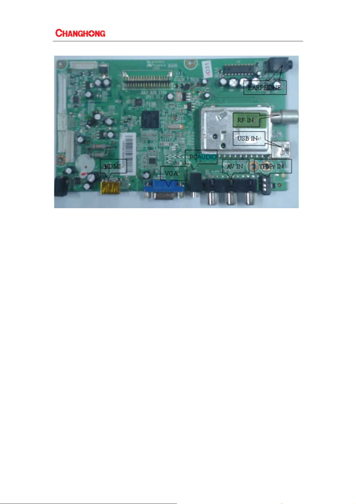
2.2 Introduction of terminals (practicality photos)
ATTENTION:
1. HDMI and YPbPr support to 1080P (max. resolution)。
2.The recommendation resolution of PC input is 1024X768。
3. AV output supports TV input /AV output,AV input /AV output。
5
Page 6
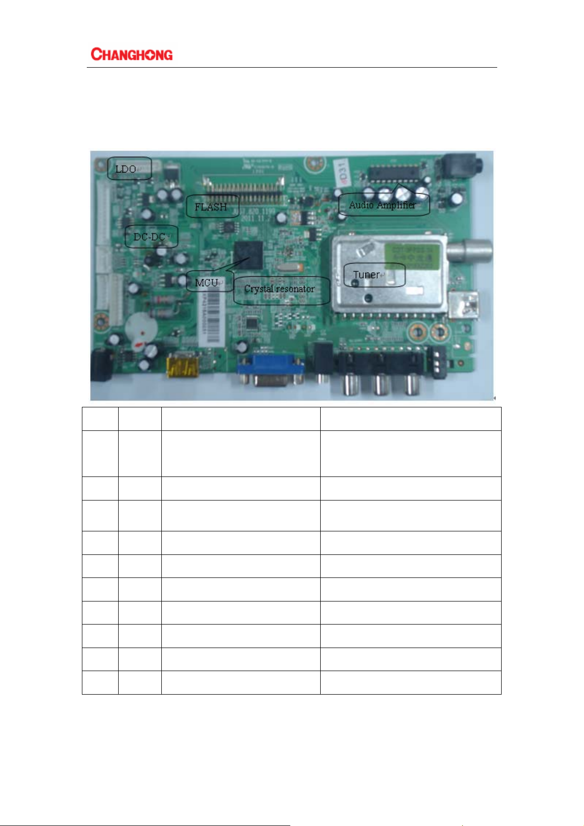
p
Chapter3: Main chip functions and brief introductions of power
supply
3.1 Main IC and functions of LS0B
No. Item no. Model Main Function
Processor with Video Decoder,
1 U200 MST6M182VG-LF-Z1
2 A001 CDT-3BP4I1-34
3 U202 EN25Q32A-100HIP
4 U806 SY8008B
5
6 U804 LR1117/A-2.5$AZ1117H-2.5TR
6 U805 LR1117/A-1.8$AZ1117H-1.8TRE1
9 U701 SA7454 Audio Amplifier
10 Y200 JA18AS-24MHZ Crystal resonator
11 U001 AS7805ADTR-E1
U802、
U803
LR1117/A-3.3$AZ1117H-3.3TR
MCU,HDMI decoder,LVDS transmiter
etc.
Tuner, output dfferential IF signal
Flash memory, Place the main control
rogram
DC-DC,DC voltage converter
LDO(three terminal regulator)
LDO(three terminal regulator)
LDO(three terminal regulator)
LDO(three terminal regulator)
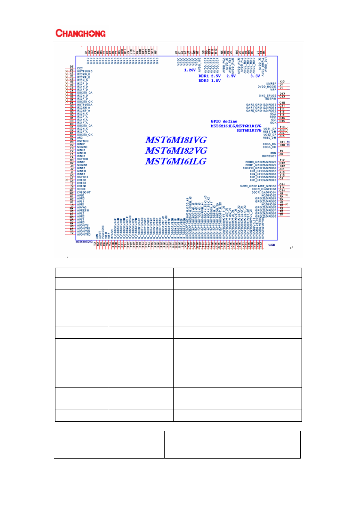
3.2 Pin function description of LS0B main chip
3.2.1: The main chip MST6M182VG-LF-Z1 instraction
6
Page 7
3.2.2 :Pin function of CDT-3BP4I1-36 tuner:
No.
Terminal name Description
1 NC Not connected
2 AGC RF AGC output 0~4V
3 VCC Supply voltage 5V
4 GND Ground
5 VT Not connected
6 AS Address select
7 SCL Clock
8 SDA Data
9
10
11
12
IF1 IF output 1
IF2 IF output 2
TU 33V
NC Not connected
3.2.3:Pin function of EN25Q32A flash memory
No. Terminal name Description
1 CS# Chip Enable
7
Page 8
2 DO(DQ1) Serial Data Output(Data Input output1)
3 WP#(DQ2) Write Protect(Data Input output2)
4 VSS Ground
5 DI(DQ0) Serial Data Input(Data Input output0)
6 CLK Serial Clock Input
7 NC(DQ3) No Connect(Data Input output3)
8 VCC Supply Voltage(2.7-3.6V)
3.2.4: Pin function of MP1482 (DC-DC converter):
No.
Terminal name Description
1 BS High-Side Gate Drive Boost Input
2 IN Input
3 SW Output
4 GND Ground
5 FB Output voltage feedback
6 COMP Calibration compensation
7 EN Enable switch
8 SS Soft start control
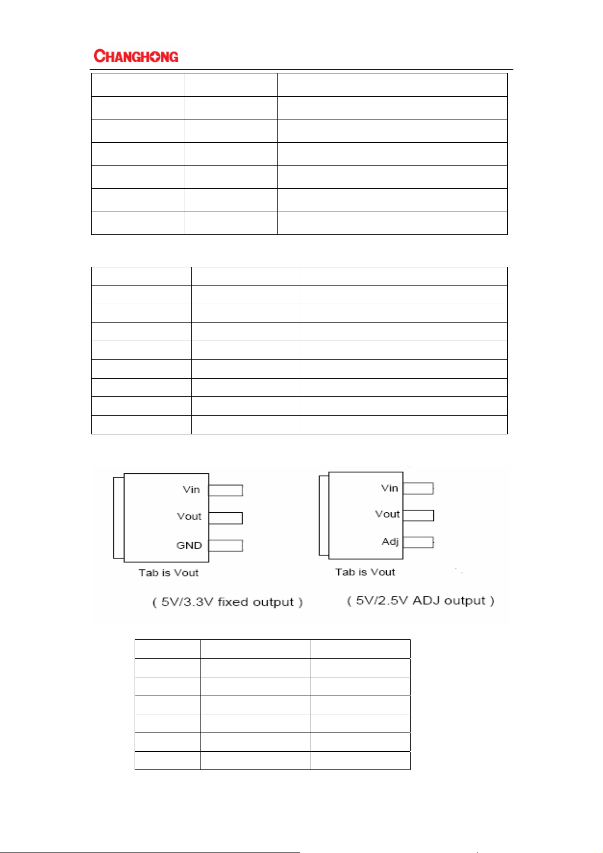
3.2.5 :Pin function of 1117/A-3.3 and 1117/A-2.5 :
3.2.6: Pin function of AO4803 (Dual-channel enhanced MOSFET) :
No.
Terminal name Description
1 S2 Source 2
2 G2 Gate 2
3 S1 Source 1
4 G1 Gate 1
5,6 D1 Drain 1
7,8 D2 Drain 2
8
Page 9
3.2.7: Pin function of SA7454/TDA1517P(audio amplifier):
No.
Terminal name In/Out
1 /CS I Input selection
2 DO O Data Output
3 WP# I Write protection
4 VSS Ground
5 DI I/O Date Input/Output
6 CLK I Serial clock input
7 NC I Output remains
8 VCC Power
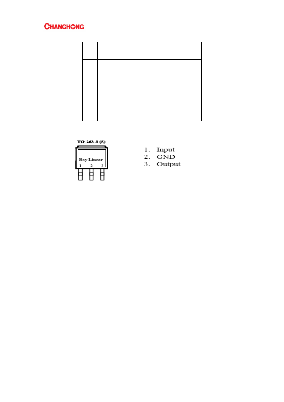
3.2.8:Pin function of AS7805 :
Description
9
Page 10

3.3 Brief introduction of power board
12V
12V
12V
GND
GND
GND
5V
5V
AC IN
Power input and output parameters are as follows:
1、Input rate voltage: 110/220Vac
2、Input voltage range: From 90Vac to 264Vac
3、Enter the rated frequency: 50/60Hz
4、Input frequency range: 50/60 +/-3Hz
5、Maximum input current: 2A max
6、Inrush current: 60Ap-p max : 60Ap-p max/220VAC
7、efficiency: 75% min
8、No Load Power Consumption: 0. 75Wmax
Power output parameters are as follows:
1、Output voltage
Channel Parameter Min(V) Nom(V) Max (V)
DC Output
+12V +11.4V +12.0V +12.6V
+5V +4.75V +5.0V +5.25V
2、Output Current and ripple & noise
Channel Parameter Min(A) Nom(A) Max (A) Ripple&noise(mV)
DC Output
+12V 0A 2.0A 2.5A 120mV
+5V 0A 2.0A 3.0A 50mV
10
Page 11

Chapter4: The chassis frame diagram, mainboard power supply
systems, mainboard interface definition and the waveform of key
points
This chapter mainly introduces the chassis frame diagram, power supply system, interface
definition and each key point’s wave shape.
4.1 The chassis frame diagram
4.2 Power supply system
Power board has two kinds of output voltage: +12and+5
4.2.1 the logic relation diagram of main board power
U811
MP1484
Q808
AO3401
+12VStb
CON801
PIN 6,7,8
U701
U001
U809 R008
AO8401 L001
11
External LED backlight driver 12V or12V power supply for the inverter
VCC_PANE
DVD 12V supply power
TDA1517 12V supply power
5V Tuner power
33V, RFH (high frequency head)
+12V_Normal
CON602
RY600
Page 12

Q808
AO3401
+5VStb
CON801
AO8401
PIN1,2
U809
U802
1117-3.3
VCC_PANEL
+5V_NORMAL
+3.3V_Standby
U806
+1.2V_VDDC 2
U403
5VPI1 SGM330 power
L201
U804
L200
U805
+5V NORMAL
+5V_USB
ADC2P5
+2.5V_Normal
+2.5V_PGA
AVDD_DDR
CON
DVD+5V power
AVDD_33
U803
+3.3V_Normal
VCC_PANEL
4.2.2 Pin voltage of the voltage adjustor on the mainboard
Item
U806 U805 U802 U803 U804 U811 U809 U001
Input voltage
Output voltage
5V 5V 5V 5V 5V 12V 12V/5V 12V
1.2V 1.8V 3.3V 3.3V 2.5V 5V 12V/5V 5V
4.2.3Interface definition
12
Page 13

4.3 The waveform of key points
13
Page 14

Chapter5: Software upgrade tooling , software upgrade instructions ,
software initialization , parameter setting , software version and
screen matching instructions
5.1 Software upgrade tooling
There are three kinds of using upgrade tooling:
1.Use the combined interface(the parallel port) upgrade tooling :use the upgrade program: ISP_
Tool V4.0.5.exe(and higher versions)
2.Use USB interface upgrade tooling , use the upgrade program : versions higher than ISP Tool
V4.3
3. Use the USB upgrade
Combined interface or USB
Computer Upgrade tooling LCD TV
VGA
5.2 Software upgrade instructions
5.2.1 Tooling upgrade
1. Driver Installation: Upgrade tooling connected to the computer via USB, the first connection
will be prompted to find the hardware, follow the prompts to install the driver, Driver file from the
attachment "usb-update TOOL-DRIVER" folder inner tube MSTAR name of the subfolder word
where you can, you are prompted three times, three times to be installed.
2. After installing the driver tooling, tooling and TV connected (switched on), open the upgrade
tool "ISP_Tool V4.3.9.4.exe" (Note: The following chart version of the tool used for the
interception chart, the upgrade is still using V4 .3.9.4 version), run the upgrade program
14
Page 15

Cancel the selection in the red line frame of the above picture, result showed as follows:
15
Page 16

3. Click the button connect on the toolbar first, if normal, system wills feedback a dialog box
shows the flash style of the machine chassis As follows.
4. Click the button Read on the toolbar, a button read appears , click it and then select the upgrade
file "CH-P06U (VC)-V1.15-YD12.bin"
16
Page 17

5. Click the button Auto, and check the options according to the following picture.
6. Click the button connect on the toolbar, if has been connected successfully, there will popup a
dialog box prompts the Device Type, click OK and then click RUN.When the upgrade process
finished, a green prompt "PASS"will appear in the progress bar below.
5.2.2 use usb upgrade
Enter the factory menu, select Software Update to finish the upgrade.
17
Page 18

5.3 Software initialization
After finishing the software upgrading ,enter into the factory menu ,select Default, clear
EEPROM.
The system will automatically boost after clearing EEPROM.
18
Page 19

5.4 Software version
Related program information can be read from the software version, which is useful to
professional to know the software’s states.
19
Page 20

Chapter6: typical faults and maintenance procedures
6.1 Can’t be booted
→
check every voltage accord
to the mainboard power logic
diagram
check if 5V,12V
works normally
change power board
Change the
screen
check the circuit related to
the mainboard
check if the reset circuit
works normally
check if 5V,12V are too
rush when boot
black screen
check the
backlight
voltage
check the screen line
Boot failure Check if controller receiver works normally
check if the working condition
of main IC is normal
check if the service circuit
works normally
check if each chip on the assemble
line works normally
no image
flowery or white screen
check the screen and the
mainboard crossly
change the screen or
examine the mainboard
change the main chip
Check if the assemble
works normally
no sound
check if there is signal
entering into the main
chip of each source
Change the
main chip
check if FLASH
works normally
change the chip
check if there is
signal output from
the main chip
Check if there is
output from the
amplifier
20
Page 21

6.2 problems of the Key parts of the mainboard
NO. phenomenon principle
L001、D002、
Q001
U403、U404 YPbPr, DVD, SART, VGA no
Tuning can only search the
low frequency
plan or lack of color channel
33V 12V conversion circuit,tuner use
U403, U404 is a video switch, if damaged,
the signal can not enter the main chip
21
Page 22

6.3 Common problems for your reference:
To speed you to diagnose and solve problems, we offered some common problems’ solutions as
follows for your reference.
Symptoms Possible Reason Solutions
No picture, no sound, and no
indicator light on
normity Picture and sound
Picture is spotted or with snow
No picture, no sound and
indicator light is green
Blue screen, AV or SVIDEO is
displayed
Picture is unclear or shaking or
with black horizontal strips (in
VGA mode)
VGA picture is not centered
No sound
VGA picture display with
improper color
HDMI source, with snow pixel
of full screen
The remote control does not
work
1.The power cord is not plugged in
2.The power is off
1.Contrast, sharpness, and color are
set improperly
2.Color system is improperly
3.Sound system is improperly
Signal source is low-grade or the
signal cord is in a lower quality
Contrast, brightness, color and
volume are all in the minimum value
or TV is in mute mode.
The signal cable is not correctly
connected.
There is no signal input or the video
cable is not connected or incorrectly
connected
VGA picture is not correctly adjusted.
There is no audio signal input or audio
cable is not connected correctly
The color temp is adjusted incorrectly
by user
The signal source is not normal
Batteries are improperly installed or
exhausted
1.Plug in the power cord
2.Turn the power on
1.Adjust the numerical
value of Contrast,
sharpness, and color
2.Set the Color system to
the country
broadcasting standard
3.Set the Sound system
to meet the country’s
broadcasting standard
Use the qualified signal
cord
Adjust the value of
contrast, brightness,
color and volume
Connect the signal cable
correctly
Connect the video cable
correctly
Enter “SETUP” menu,
select “Auto Tracking”
item to perform
automatic calibration
and adjust “Phase” to
solve the problem
Connect the audio cable
correctly
Readjust the color
temp, or select the
original color setting
Plug the HDMI cable
again
1. Make sure the positive
and the negative
polarities are correct.
2.Check if there is a
loose contact between
the batteries and the
springs
3.Replace the batteries
22
Page 23

Chapter7: Spare Part Lists
The introduction of spare parts are for reference only, modification of parameters will not be
informed any more. For accurate data and related specifications, please consult the newest data of
our company.
Number Name Model number
1. Main Board
2. Remote receiving board JUG6.695.491-01 0.5
3. Key board JUG6.694.528-06 0.5
4. Power board PW52057B 5
5. LCD panel HT185WX1-100 0.1
6. Tuner CTD-3BP4I1-36 0.5
7. Dynamoelectric speaker YDT3070-C1-5W-4Ω 2
8. Video signal processing chip
9. Audio amplifier
JUG6.690.968
MST6M182VG-LF-Z1/
AS7454/TDA1517
The damageable
percentage(‰)
1
1
1
23
Page 24

Chapter8: Factory mode parameter setting instructions and notes
8-1 Enter into the factory mode
Switch on TV set, and make it works normally:
① Press 【SOURCE】 key on the remote control
② Press number keys “3”、“1”、“3”、“8” on remote control to enter password. Finish
entering the factory mode. If you want to quit the factory mode, Please. press【Power】
key to switch off the TV.
⑴ Factory menu displays as bellow:
⑵
Adjust item Adjust content Adjust method Remark
SPECIAL SET System setting 【﹥】、【﹤】key
Default Clear EEPROM 【﹥】、【﹤】key
AGING MODE Aging switch 【﹥】、【﹤】key
PANEL CONTROL Panel parameter select 【﹥】、【﹤】key
ADC ADJUST ADC adjustment 【﹥】、【﹤】key YPBPR、PC available
W/B ADJUST
Switch the five state
PICTURE Picture mode 【﹥】、【﹤】key
SOUND Sound mode 【﹥】、【﹤】key
NON LINEAR
“Standard、Soft、User、
Home、Vivid” at each
source
Switch the five
state“ Theater、Music、
Sport、User、Standard” at
each source
COLOR Color temperature 【﹥】、【﹤】key
SSC Spread spectrum setting 【﹥】、【﹤】key For EMC use
VIF1 【﹥】、【﹤】key
SW INFORMATION 【﹥】、【﹤】key Software Information
Software Update 【﹥】、【﹤】key Upgrade
(2) Use the key 【▲】/【▼】on remote control to select items that need to adjust,,use the key 【﹥】
/【﹤】to adjust them.
Submenu content:
SPECIAL SET
adjust item adjust value remark
INPUT SOURCE preset AV SOURCE lines
LANGUAGE OSD language select
WHITE PATTER OFF
POWER OFF
CHANNEL
AGING MODE OFF
switch on/off :once mode or twice
Tuner paramete
adjustment
mode
24
Page 25

HOTEL MODE ON
TUNER TYPE CTD_3BP4I1_32 select tuner’s type
Audio Type select the output power of speaker
MENU MENU switch
USB CLONE no need of adjustment
UART DEBUG ON
OVERSCAN HK
LOGO OFF LOGO switch
PICTURE
adjust item adjust value remark
MODE standard select the picture mode to adjust
BRIGHTNESS 50 no need of adjustment
CONTRAST 50 no need of adjustment
COLOR 50 no need of adjustment
SHARPNESS 50 no need of adjustment
TINT 50 no need of adjustment
COLOR
SOUND
adjust item adjust value remark
TREBLE
SPDIF MODE
PRESCALE
adjust item adjust value remark
F_color 0 no need of adjustment
ICC_color saturation no need of adjustment
IBC_Bringtness Bringtness no need of adjustment
IHC_HUE tincture no need of adjustment
MODE
BASS
Theater select the sound mode
75 no need of adjustment
25 no need of adjustment
120HZ
500HZ
1.2KHZ
7.5KHZ
12KHZ
55 no need of adjustment
65 no need of adjustment
70 no need of adjustment
65 no need of adjustment
60 no need of adjustment
IF output no need of adjustment
AV L
36(Automatic volume control) no need of adjustment
no need of adjustment
25
Page 26

NON LINEAR
adjust item adjust value remark
MODE TV display the present signal source
PICTURE MODE standard select the picture mode to adjust
BRIGHTNESS CURVE brightness no need of adjustment
CONTRAST CURVE contrast no need of adjustment
SATURATION CURVE saturation no need of adjustment
HUE CURVE hue no need of adjustment
SHARPNESS CURVE sharpness no need of adjustment
VOLUME CURVE volume no need of adjustment
TREBLE treble no need of adjustment
BASS bass no need of adjustment
BACK LIGHT Back light no need of adjustment
8.2 Setting method of factory menu
⑴ Select the setting item
Operators can choose setting item with【P+】and【P-】key, font with background display means
the item has been chosen. Press【V+】key to enter sub directory. Use 【P+】and 【P-】keys on
remote control to select up and down, then use【V+】and【V- 】keys to set.
(2)Most of the menu functions are open under factory mode, if needed , item checking and effect
test can be done by using menu .
(3) TV signal switching can be done by directly pressing the number keys in factory mode .Press
【MENU】to back to the parental catalog ,press【EXIT】 to quit factory mode.
26
Page 27

Chapter9: Instructions of simple factory debugging specification
9.1 Clear EEPROM, and set the parameters after upgrading according to the
upgrade instructions.
9.2 Check the image and sound of each channel/source are normal (or abnomal).
27
 Loading...