

Page 1

(with price)
INDEX
POCKET TELEVISION
TV-350C
OCTOBER 1994
Page
Specifications.............................................................................................2
Block Diagram ...........................................................................................3
Adjustment
Linear PCB......................................................................................... 4
Printed Circuit Boards................................................................................8
Wiring Diagram........................................................................................10
Electrical Parts List ..................................................................................11
Mechanical Parts List...............................................................................17
Exploded Views / Disassembly................................................................ 18
Schematic Diagrams and Waveforms .....................................................19
R
Page 2
SPECIFICATIONS
Item Specification
Reception Channels VHF: Ch 2 ~ 12 ch UHF: Ch 21 ~ 69
Power Voltage DC 6.0 V
Power Consumption Approx. 3.0 W
Current Consumption Approx. 500 mA
Battery Life (with alkaline batteries) Approx. 3.0 hours
Batteries : 4 AA size batteries
Power Supply Car adaptor : CA-K65
AC adaptor : AD-K65
Connection Terminals Earphone jack : 3.5ø mini
External power jack : 6.0 V DC IN
Screen Size 1.6 inches
No. of Picture Element 39,600 (110 × 360) dots
Dimensions 122 mm (H) × 66 mm (ø)
Weight 210 g excluding batteries
7.4 oz excluding batteries
Options AC adaptor : AD-K65
Car adaptor : CA-K65
— 2 —
Page 3
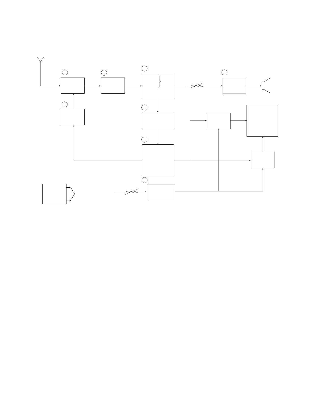
Antenna
BLOCK DIAGRAM
Power
Supply
1 TU200 2 Q200
IF Amp.Tuner
7
IC500
Tuning
Voltage
Generator
VCC2 (3.95V±0.02V)
VCC6 (30.5 ~ 39.0V)
VCC7 (53.5 ~ 72.5V)
VEE1 (-6.3 ~ -7.9V)
VR800
Brightness
Control
3 IC200
Video
Sound Det.
FM
AFT Circuit
AGC Circuit
5
6
8 Q800 ~ Q806
IC300
Chroma
Circuit
IC700
OSC
Display
Control
A-D Converter
Auto-Tuning
Control
Display
Voltage
Generator
VR600
Volume
Control
4 IC600 Speaker
Audio
Amp.
Common
Driver
LCD
Segment
Driver
1 — Color Tuner: TU200 TEPE5-01
Selects a desired radio wave and changes it to the video IF signal.
2 — Video IF Amp.: Q200 2SC4238
Amplifies the video IF signal output from the tuner TU by 10 times (20dB).
3 — Video Det./Sound Det./FM Det./AFT/AGC: IC200 M51348FP
Eliminates the carrier wave in the video IF signal, and picks up the video signal and the sound IF signal.
Also, the sound signal is picked up from the sound IF signal by FM detection.
4 — Audio Amp.: IC600 NJM2070M
Sound amplification.
5 — Chroma Circuit: IC300 M52045FP
Generates the tricolor (red, green, and blue) from the video signal.
6 — OSC/A-D Converter/Display control/ Auto-Tuning Control : IC700 MSM662502 GSK-640F
Converts the color signal into a digital signal.
Also, generates the clock pulse for the display and controls the display.
7 — Tuning Voltage Generator: IC500 MSC1169MS-K
Generates the tuning voltage with the tuning pulse (TU) output from 6.
8 — Display Voltage Generator: Q800 ~ Q806 2SB1218A-R, 2SD1824R, S × 2, 2SD1819A-R × 5,
2SD1824-5
Generates the display voltages V0 ~ V4 with VEE1 and VCC7 outputs from the power supply.
— 3 —
Page 4
ADJUSTMENT
Linear PCB
1) Items to Be Adjusted
Item Measuring Instrument
VCC2 voltage setting Voltmeter
Video detection coil adjustment TV signal generator, Pattern generator, Oscilloscope,
Low-pass filter
AFT coil adjustment Sweep generator, Oscilloscope, Voltmeter
Contrast adjustment TV signal generator, Pattern generator, Oscilloscope
AGC adjustment TV signal generator, Pattern generator, IF levelmeter
Clock adjustment Voltmeter
2) Adjustment and Test Point Locations
TOP VIEW
T201T200
VR100
— 4 —
Page 5
Pad IF
BOTTOM VIEW
TP7
VR200
TP2
TP3
TP4
VR700
TP6
VR301
TP5
VR300
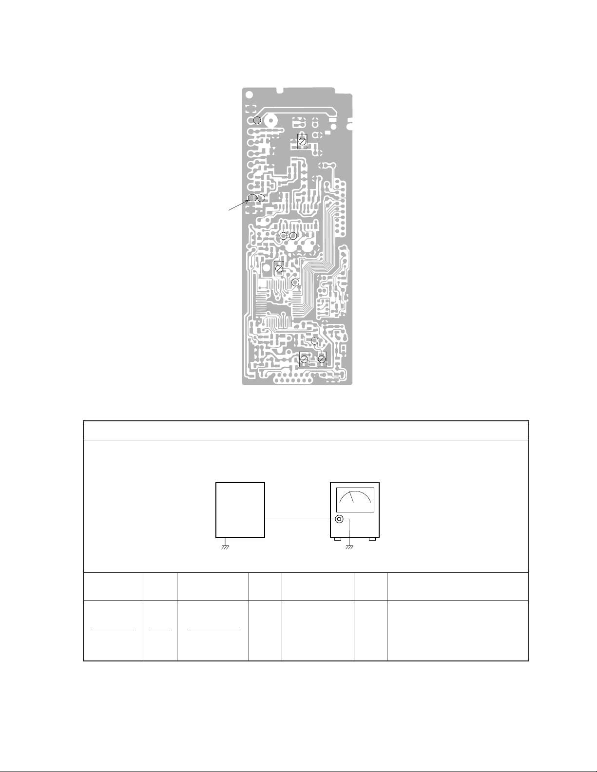
3) Equipment Connection / Procedure
VCC2 Voltage Setting
TV-350
Set
Voltmeter
Output
TP1
Input Input Input Output Output
Connection Point Signal Connection Point
Adjust Result
VR100
Voltmeter
TP1
Adjust for 3.95 ± 0.02V
reading on voltmeter.
— 5 —
Page 6
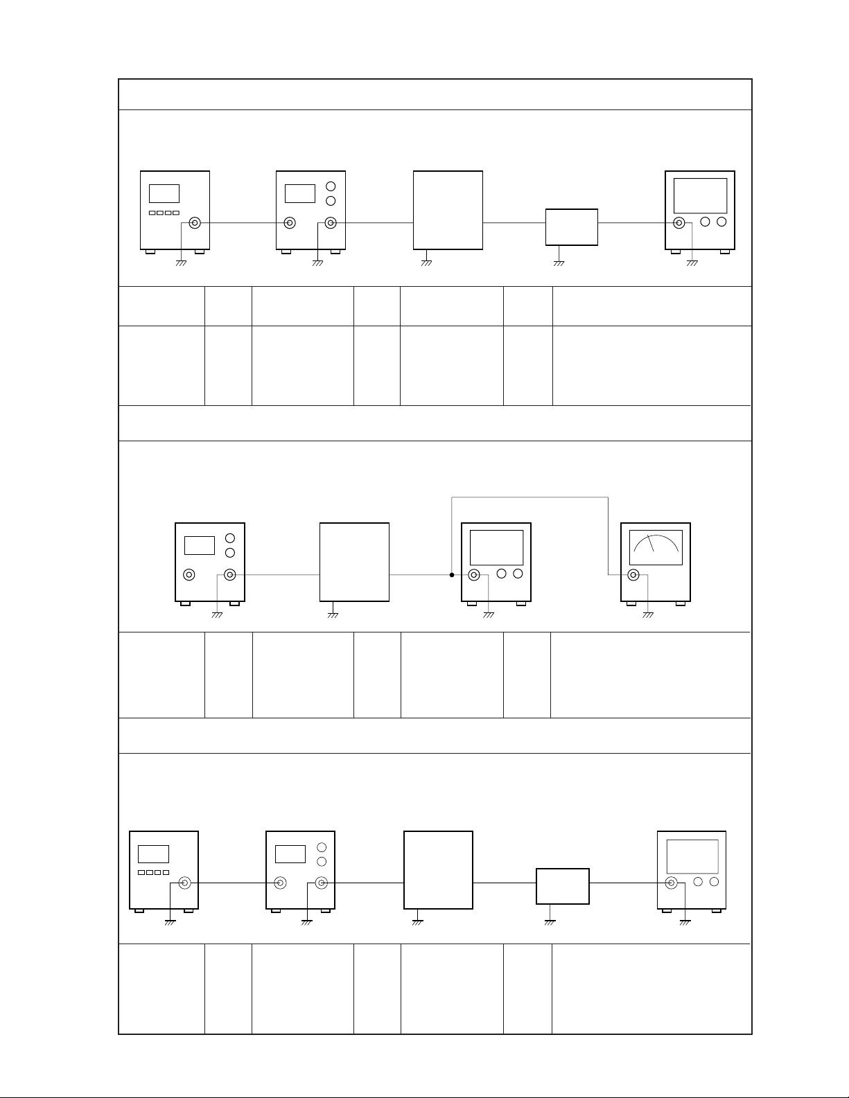
* Open soldering pad IF.
Pattern
generator
Signal
generator
Video Detection Coil Adjsutment
TV-350
Set
Input Output
Oscilloscope
Low-pass
filter
TP2
Input Input Input Output Output
Connection Point Signal Connection Point
Adjust Result
TP3
Pattern
generator
Signal
generator
TP2 T200 TP3
Color bar
38.9MHz
41 ± 3dBµ
Low-pass filter
Oscilloscope
AFT Coil Adjustment
* Open soldering pad IF.
Sweep
generator
Input
TP2
TV-350
Set
Oscilloscope Voltmeter
Output
TP4
R=180 ohm
C=0.01 µF
Adjust for DC level at mini-
38.9 ± 5MHz
Sweep
generator
(Sweep) Marker:
TP2 T201 TP4
38.9MHz
70dBµ
* Open soldering pad IF.
Pattern
generator
Pattern
generator
Signal
TP2 VR300 TP5
Color bar
38.9MHz
70dBµ
generator
Signal
generator
Voltmeter
Oscilloscope
Contrast Adjustment
TV-350
Set
Input
TP2
Oscilloscope
Adjust for 1.8 ± 0.2V reading on
voltmeter.
Confirm that the marker is at
the middle of S-curve on oscilloscope.
Oscilloscope
Low-pass
filter
Output
TP5
R=100 ohm
C=2700 pF
Adjust step form wave to read
0.75 ± 0.05 Vp-p.
— 6 —
Page 7
AGC Adjustment
Pattern
generator
Signal
generator
TV-350
Set
Input Output
TP7
Input Input Input Output Output
Connection Point Signal Connection Point
Adjust Result
TP2
Pattern
generator
TV Signal
TP7 TP2
Color bar
65 ± 5 dBµ
VR200
IF levelmeter
generator
Tint Adjustment
* Open soldering pad IF.
Pattern
generator
Pattern
generator
Signal
TP2 TP3
Signal
generator
Color bar
38.9MHz
70 dBµ
Input
TP2
VR301
TV-350
Set
Output
TP3
Low-pass filter
Oscilloscope
generator
IF levelmeter
Adjust for 81 ± 1 dBµ reading
on the IF levelmeter
Oscilloscope
Low-pass
filter
R=100 ohm
C=2700 pF
Adjust VR301 so that the difference between pulse A and
B is less that 0.1V.
Pulse A Pulse B
Clock Adjustment
TV-350
Set
Output
TP6
VR700 TP6
Voltmeter
— 7 —
Voltmeter
Adjust for 1.00 ± 0.05V
reading on voltmeter.
Page 8

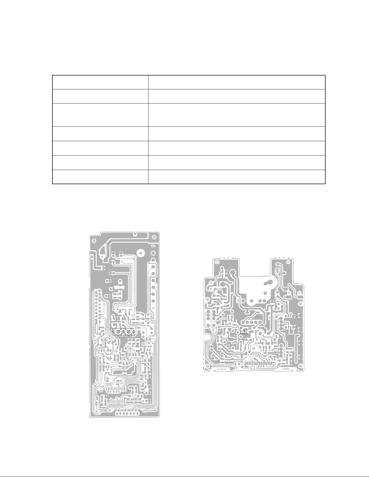
PRINTED CIRCUIT BOARDS
Linear PCB
(Top View)
C202
C208
C299
C207
C808
C205
C806
C262 C263
C765
R740
R803
C850
D800
C800
D805
Q805
R830
R824
R823
C346
R322
C345
C810
Q804
D700
C700
IC300
C210
F200
R208
R222
C247
R223C259R241
R239
T201 T200
R820
D803
Q806
R833
R825
R827
C845
R809
R808
R810
C761
R312
H300
C755
R326
R257
C758
R730C756
C351
R331
C347
TU200
R230R229
F202
R236
R733
C760
D705
R703
R706
R302
R330
R325
C350
L202
R224
R701
R718
R719
R727
R726
R725
C335
C305
C309
F201
L102
D703
PW PCB
(Top View)
C180
C182
R185
R184
Q100
Q101
C145
R117
R183
C135
R101
Q111
VR100
C112
D152
T950
R100
D100
R500 R502
R545R541
C545
C530
R504
R607
R606
IC600
C600
R612
C630
C641
R611
R610
C641
CN100
KY PCB
(Top View)
SW701
SW702
— 8 —
Page 9

PW PCB
(Bottom View)
CN600
Linear PCB
(Bottom View)
JK600
VR600
VR800
R645
C606
C603
C645
C550
R950
IC500
Q950
R550
D155
C925
Q951
C146
D154
R531
FU100
R111
D150
C154
C100
C118
JK101
D185
C103
C140
R115
L101
C110
C114
SW100
R705
R303
C332
Q300
C232
C233 R207
R704
R310
R209
C235
R202
R205
R203
R201
R225
C268
C331
R133
C230
C236
C237
C249
R246
R247
C269
IC700
R307
R301
R306
R305
R336
R210
Q200
VR700
R335
L200
IC200
R734
C751
C303
R204
C239
R342
R710
VR200
R214
C240
C246 R212
C243
C261 C264
C750
C340
C338
VR301
R220
C245
C740
C742
Q803
C741
VR300
R343
JK200
R818
R817
R816
R840
R815
Q802 Q800
Q801
R709
R708
D707
R738
CN700
R800
KY PCB
(Bottom View)
— 9 —
C701
C702
R701
Page 10

WIRING DIAGRAM
KY PCB
4
1
4
1
115
115
PW PCB
Linear PCB
— 10 —
Page 11

ELECTRICAL PARTS LIST
Linear PCB Assembly NO. 1
FOB Japan
N Item Code No. Parts Name Specification M N.R.Yen R
Unit Price
Capacitors
C202 2800 9182 Electrolytic 6.3RC2-47MS 20 15 C
C205 2804 9765 Electrolytic 50RC2-2R2 10 18 C
C207 2800 9182 Electrolytic 6.3RC2-47MS 20 15 C
C208 2800 9182 Electrolytic 6.3RC2-47MS 20 15 C
C210 2804 9064 Electrolytic 16RC2-10 10 9 C
C230 2892 0059 Chip GR40Y5V103Z50PT 10 9 C
N C232 2897 2114 Chip EMK212F105Z-T 20 10 C
C233 2892 0059 Chip GR40Y5V103Z50PT 10 9 C
N C234 2897 2114 Chip EMK212F105Z-T 20 10 C
C235 2897 0994 Chip GR42-6Y5V334Z50PT 20 19 C
C236 2892 0059 Chip GR40Y5V103Z50PT 10 9 C
C237 2892 0059 Chip GR40Y5V103Z50PT 10 9 C
C239 2892 0113 Chip GR40CH150J50PT 10 10 C
C240 2892 0059 Chip GR40Y5V103Z50PT 10 9 C
C243 2892 0059 Chip GR40Y5V103Z50PT 10 9 C
C245 2892 0059 Chip GR40Y5V103Z50PT 10 9 C
C246 2892 0059 Chip GR40Y5V103Z50PT 10 9 C
C249 2892 0844 Chip GR42-6Y5V474Z16PT 20 27 C
C257 2892 0407 Chip GR40CH270J50PT 10 10 C
C259 2892 0091 Chip GR40W5R223K25PT 10 15 C
C261 2892 0890 Chip GR40PH560J50PT 20 13 C
C262 2897 0378 Chip GR40PH270J50PT 10 5 C
C263 2892 0890 Chip GR40PH560J50PT 20 13 C
C264 2892 0491 Chip GR40CH020C50PT 20 3 C
N C268 2897 2100 Chip GR40CH111J50PT 20 4 C
C269 2892 0300 Chip GR40CH470J50PT 10 10 C
C299 2892 0059 Chip GR40Y5V103Z50PT 10 9 C
C303 2897 1827 Chip tantalum EMK316B474K-T 10 22 C
C305 2804 9064 Electrolytic 16RC2-10 10 9 C
C309 2800 9182 Electrolytic 6.3RC2-47MS 20 15 C
C331 Not Used
C332 2897 0084 Chip GR42-6Y5V105Z16PT 20 3 C
C335 2892 0865 Chip GR40CH471J50PT 20 15 C
C338 2892 0016 Chip GR40W5R102K50PT 10 11 C
C340 2892 0083 Chip GR40W5R103K50PT 10 14 C
C345 2897 0112 Chip GR40W5R562K50PT 20 12 C
C346 2897 0973 Chip GR40W5R683K25PT 10 16 C
C347 2897 0973 Chip GR40W5R683K25PT 10 16 C
C350 2892 0326 Chip GR40CH101J50PT 10 11 C
C351 2897 0245 Chip GR40CH180J50PT 20 6 C
C700 2800 9182 Electrolytic 6.3RC2-47MS 20 15 C
C740 2892 0040 Chip GR40Y5V104Z25PT 10 14 C
C741 2892 0040 Chip GR40Y5V104Z25PT 10 14 C
C742 2892 0040 Chip GR40Y5V104Z25PT 10 14 C
C750 2892 0458 Chip GR40CH220J50PT 20 6 C
C751 2892 0458 Chip GR40CH220J50PT 20 6 C
C755 2892 0903 Chip GR40UJ270J50PT 20 10 C
C756 2892 0059 Chip GR40Y5V103Z50PT 10 9 C
C758 2892 0059 Chip GR40Y5V103Z50PT 10 9 C
C760 2892 0237 Chip GR40W5R222K50PT 20 9 C
C761 2892 0059 Chip GR40Y5V103Z50PT 10 9 C
Notes: N – New parts
M – Minimum order/supply quantity
R – Rank
— 11 —
Page 12

Linear PCB Assembly NO. 2
FOB Japan
N Item Code No. Parts Name Specification M N.R.Yen R
Unit Price
C765 2897 0553 Chip GR40Y5V224Z16PT 10 24 C
C800 2800 9182 Electrolytic 6.3RC2-47MS 20 15 C
C806 2800 9945 Electrolytic 50RC2-4R7MS 20 14 C
C808 2804 9765 Electrolytic 50RC2-2R2 10 18 C
C810 2804 9212 Electrolytic 50RC2-1 10 9 C
C840 2897 0126 Chip GR40CH221J50PT 20 9 C
C845 2892 0288 Chip GR40CH100D50PT 10 10 C
C850 2897 0728 Chip GR40Y5V104Z50PT 20 9 C
Connectors
N CN100 3501 8239 Connector 52233-1510 5 67 C
CN700 3501 3234 Connector 52030-2020 5 85 C
Diodes
D700 2390 1470 Chip MA143A-(TX) 20 16 C
D703 2390 1470 Chip MA143A-(TX) 20 16 C
D705 2390 1358 Vari-cap MA329-(TX) 10 30 C
D707 2360 0854 Chip, Zener MA3100-M(TX) 10 17 C
D800 2360 1652 Chip, Zener MA3075-H(TX) 10 14 C
D803 2390 1470 Chip MA143A-(TX) 20 16 C
D805 2390 1477 Chip MA142WA-(TX) 20 10 C
Filters and Traps
F200 3025 0189 SAW filter SAF38.9MZ60Z 1 150 C
F201 3025 0728 SIF filter SFSL5.5MDB12 10 33 C
F202 3851 1148 Ceramic discriminator CDSL5.5MC30B12 5 45 C
Oscillator
H300 2590 0651 Crystal oscillator HC-49U-C 1 110 C
ICs
IC200 2114 1827 Linear M51348FP-T1 1 190 B
IC300 2114 3311 Linear M52045FP-T1 1 300 B
IC700 2011 3514 Linear MSM6625-02GSK-640F 1 280 B
Jack
JK200 3501 5439 Jack HSJ1456-01-210 1 27 C
Inductors
N L102 3841 1162 Inductor LAL02VE220J 20 17 C
L200 3013 0686 Chip MLF2012DR82K-TP 10 30 C
N L202 3841 1155 Chip LAL02VE8R2J 20 17 C
N L705 3841 1148 Chip LAL02VE270J 20 17 C
Transistors
Q200 2252 0707 Chip 2SC4238-(TX) 10 17 C
Q300 2251 0189 Chip 2SB1218A-R(TX) 10 10 C
Q800 2253 0133 Chip 2SD1819A-R(TX) 10 12 C
Q801 2251 0189 Chip 2SB1218A-R(TX) 10 10 C
Q802 2253 0133 Chip 2SD1819A-R(TX) 10 12 C
Q803 2253 0133 Chip 2SD1819A-R(TX) 10 12 C
Q804 2253 0133 Chip 2SD1819A-R(TX) 10 12 C
Q805 2253 0532 Chip 2SD1824-R,S(TX) 20 30 C
Q806 2253 0133 Chip 2SD1819A-R(TX) 10 12 C
Resistors
R133 2791 1617 Chip ERJ-6GEYJ100V 20 3 C
R201 2791 2117 Chip ERJ-6GEYJ820V 20 4 C
R202 2791 0580 Chip ERJ-6GEYJ392V 10 4 C
R203 2791 0712 Chip ERJ-6GEYJ152V 20 4 C
R204 2791 0831 Chip ERJ-6GEYJ681V 20 4 C
R205 2797 2079 Chip ERJ-6GEYJ120V 20 3 C
R207 2791 2117 Chip ERJ-6GEYJ820V 20 4 C
Notes: N – New parts
M – Minimum order/supply quantity
R – Rank
— 12 —
Page 13

Linear PCB Assembly NO. 3
FOB Japan
N Item Code No. Parts Name Specification M N.R.Yen R
Unit Price
R208 Not Used
R209 2791 0313 Chip ERJ-6GEYJ103V 10 5 C
R210 2791 0305 Chip ERJ-6GEYJ472V 20 3 C
R212 2791 0720 Chip ERJ-6GEYJ222V 20 3 C
R214 2791 0769 Chip ERJ-6GEYJ563V 20 3 C
R220 2792 0110 Chip jumper ERJ-6GEYOR00V 20 3 C
R222 2791 0696 Chip ERJ-6GEYJ470V 20 4 C
R223 2791 0615 Chip ERJ-6GEYJ154V 10 5 C
R224 2797 1127 Chip ERJ-6GEYK475V 20 3 C
R225 2797 1624 Chip ERJ-6GEYJ102V 20 3 C
R229 2791 2176 Chip ERJ-6GEYJ471V 20 3 C
R230 2791 1131 Chip ERJ-6GEYJ271V 20 3 C
R236 2791 2044 Chip ERJ-6GEYJ124V 20 3 C
R239 2791 0734 Chip ERJ-6GEYJ272V 20 3 C
R241 2791 0607 Chip ERJ-6GEYJ333V 20 4 C
R246 2797 0245 Chip ERJ-6GEYJ181V 20 2 C
R247 2797 0014 Chip ERJ-6GEYJ821V 20 3 C
R301 2791 1625 Chip ERJ-6GEYJ391V 20 4 C
R302 2791 1579 Chip ERJ-6GEYJ474V 10 4 C
R303 2791 0720 Chip ERJ-6GEYJ222V 20 3 C
R305 2791 0831 Chip ERJ-6GEYJ681V 20 4 C
R306 2797 0028 Chip ERJ-6GEYJ683V 20 3 C
R307 2791 0831 Chip ERJ-6GEYJ681V 20 4 C
R310 2791 1579 Chip ERJ-6GEYJ474V 20 4 C
R312 2791 0815 Chip ERJ-6GEYJ102V 20 5 C
R322 2791 0607 Chip ERJ-6GEYJ333V 20 4 C
R325 2791 1684 Chip ERJ-6GEYJ183V 20 3 C
R326 2797 1015 Chip ERJ-6GEYK225V 20 3 C
R330 2797 0014 Chip ERJ-6GEYJ821V 20 3 C
R331 2791 2176 Chip ERJ-6GEYJ471V 20 3 C
R335 2791 0750 Chip ERJ-6GEYJ223V 20 6 C
R336 2797 0028 Chip ERJ-6GEYJ683V 20 3 C
R342 2792 0110 Chip jumper ERJ-6GEYOR00V 20 3 C
R343 2792 0110 Chip jumper ERJ-6GEYOR00V 20 3 C
R701 2791 2095 Chip ERJ-6GEYJ682V 20 3 C
R703 2797 0035 Chip ERJ-6GEYJ105V 20 4 C
R704 2791 2141 Chip ERJ-6GEYJ273V 20 4 C
R705 2791 0769 Chip ERJ-6GEYJ563V 20 3 C
R706 2791 1650 Chip ERJ-6GEYJ122V 20 3 C
R708 2791 1650 Chip ERJ-6GEYJ122V 20 3 C
R709 2791 1650 Chip ERJ-6GEYJ122V 20 3 C
R710 2797 2191 Chip ERJ-6GEYK6R8V 20 3 C
R718 2792 0110 Chip jumper ERJ-6GEYOR00V 20 3 C
R719 Not Used
R725 2797 0245 Chip ERJ-6GEYJ181V 20 3 C
R726 2797 3304 Chip ERJ-6GEYG511V 20 3 C
R727 2797 1624 Chip ERJ-6GEYG102V 20 3 C
R730 2791 2079 Chip ERJ-6GEYJ562V 20 3 C
R733 2791 0777 Chip ERJ-6GEYJ104V 10 5 C
R734 2791 0866 Chip ERJ-6GEYJ334V 10 4 C
R738 2791 2044 Chip ERJ-6GEYJ124V 20 3 C
R740 2791 1617 Chip ERJ-6GEYJ100V 20 3 C
R800 2791 1390 Chip ERJ-6GEYJ473V 10 5 C
R803 2791 0815 Chip ERJ-6GEYJ102V 10 5 C
Notes: N – New parts
M – Minimum order/supply quantity
R – Rank
— 13 —
Page 14

Linear PCB Assembly NO. 4
FOB Japan
N Item Code No. Parts Name Specification M N.R.Yen R
Unit Price
R808 2791 1595 Chip ERJ-6GEYJ153V 20 4 C
R809 2791 1595 Chip ERJ-6GEYJ153V 20 4 C
R810 2791 1595 Chip ERJ-6GEYJ153V 20 4 C
R815 2791 2079 Chip ERJ-6GEYJ562V 20 3 C
R816 2791 0750 Chip ERJ-6GEYJ223V 20 6 C
R817 2791 0750 Chip ERJ-6GEYJ223V 20 6 C
R818 2791 0750 Chip ERJ-6GEYJ223V 20 6 C
R820 2797 1127 Chip ERJ-6GEYK475V 20 3 C
R823 2797 0672 Chip ERJ-6GEYJ684V 20 3 C
R824 2797 1953 Chip RR1220P-303-D 10 5 C
R825 2797 1960 Chip RR1220R-274-D 10 5 C
R827 2791 0607 Chip ERJ-6GEYJ333V 20 4 C
R830 2791 2052 Chip ERJ-6GEYJ224V 20 3 C
R833 2791 0750 Chip ERJ-6GEYJ223V 20 6 C
Coils
T200 3841 0700 Coil 5KAC-03A 1 60 C
T201 3841 0700 Coil 5KAC-03A 1 60 C
Tuner
TU200 1013 5315 Tuner TEPE5-01 1 820 C
Variable Resistors
VR200 2775 1211 Chip semi-fixed resistor EVM-1SSW50B54 1 27 C
VR300 2775 1260 Chip semi-fixed resistor EVM-1SSW50B14 1 26 C
VR301 2775 1260 Chip semi-fixed resistor EVM-1SSW50B14 1 26 C
N VR700 2775 1568 Chip semi-fixed resistor EVM-1SSW50B55 20 20 C
Notes: N – New parts
M – Minimum order/supply quantity
R – Rank
— 14 —
Page 15

PW PCB Assembly NO. 1
FOB Japan
N Item Code No. Parts Name Specification M N.R.Yen R
Unit Price
Capacitors
N C100 2801 8953 Electrolytic 10RC2-220 20 19 C
C103 2800 9182 Electrolytic 6.3RC2-47MS 20 15 C
C110 2804 9064 Electrolytic 16RC2-10 10 9 C
C112 2805 8777 Electrolytic 6.3RC2S-100-T36 10 16 C
C113 2805 8777 Electrolytic 6.3RC2S-100-T36 10 16 C
C114 2800 9945 Electrolytic 50RC2-4R7MS 20 14 C
C118 2805 9414 Electrolytic 100RC2-1-T36 10 15 C
C135 2897 0112 Chip GR40W5R562K50PT 20 12 C
C140 2897 0259 Chip GR40W5R332K50PT 20 7 C
C145 2892 0016 Chip GR40W5R102K50PT 10 11 C
C146 2897 1505 Chip GR40CH101J200PT 20 13 C
C154 2892 0059 Chip GR40Y5V103Z50PT 10 9 C
C180 Not Used
C182 2892 0040 Chip GR40Y5V104Z25PT 10 14 C
C545 2897 0693 Chip GR40W5R333K25PT 10 12 C
C550 2897 0021 Chip GR40Y5V683Z50PT 20 27 C
N C600 2807 7022 Electrolytic 16RC310-G12 20 13 C
C603 2804 9277 Electrolytic 6.3RC3100 10 26 C
C606 2804 9277 Electrolytic 6.3RC3100 10 26 C
C630 2892 0059 Chip GR40Y5V103Z50PT 10 9 C
C641 2892 0083 Chip GR40W5R103K50PT 10 14 C
C642 2892 0040 Chip GR40Y5V104Z25PT 10 14 C
C645 2892 0016 Chip GR40W5R102K50PT 10 11 C
C925 2825 0301 TF ECQ-V1H184JZ 20 26 C
N C927 2813 3402 Ceramic DE1005SL221J2K 20 16 C
Connector
N CN600 3501 8204 Connector CGP1604-0101 20 15 C
Diodes
D100 2390 1183 Chip MA142WK-(TX) 20 9 C
D150 2390 1176 Chip MA152WK-(TX) 20 8 C
D152 2390 1176 Chip MA152WK-(TX) 20 8 C
D154 2390 1183 Chip MA142WK-(TX) 20 9 C
D155 2390 1470 Chip MA143A-(TX) 10 16 C
D185 2390 1190 Chip ERA15-01Y 20 9 C
Fuses
N FU100 3632 0469 Fuse PI-251001(F10) 5 52 B
FU900 3632 0308 Temperature EYP-1BF102L 1 27 C
FU901 3632 0308 Temperature EYP-1BF102L 1 27 C
ICs
IC500 2114 0182 Linear MSC1169MS-K 1 140 B
IC600 2114 2464 Linear NJM2070M-T1 1 65 B
Jacks
JK101 3501 6846 Jack HEC2500-010110 1 35 C
JK600 3501 5439 Jack HSJ1456-01-210 1 27 C
Coil and Inductor
L101 3840 2374 Inductor EL0405SKI-101K-2 10 48 C
L950 3013 0756 Choke RCH-875-101K 5 55 C
Transistors
Q100 2251 0189 Chip 2SB1218A-R(TX) 10 10 C
Q101 2230 7011 Chip 2SD601A-R(TX) 10 22 C
Q111 2253 0308 Chip 2SD1119-R(TX) 10 37 C
Q950 2253 0308 Chip 2SD1119-R(TX) 10 37 C
Q951 2253 0308 Chip 2SD1119-R(TX) 10 37 C
Notes: N – New parts
M – Minimum order/supply quantity
R – Rank
— 15 —
Page 16

PW PCB Assembly NO. 2
FOB Japan
N Item Code No. Parts Name Specification M N.R.Yen R
Unit Price
Resistors
R100 2797 0014 Chip ERJ-6GEYJ821V 20 3 C
R101 2791 1633 Chip ERJ-6GEYJ123V 20 3 C
R111 2791 0815 Chip ERJ-6GEYJ102V 10 5 C
R115 2791 2117 Chip ERJ-6GEYJ820V 20 4 C
R117 2791 0696 Chip ERJ-6GEYJ470V 20 3 C
R183 2792 0110 Chip jumper ERJ-6GEYOR00V 20 3 C
R184 2792 0110 Chip jumper ERJ-6GEYOR00V 20 3 C
R185 2792 0110 Chip jumper ERJ-6GEYOR00V 20 3 C
R500 2797 0252 Chip ERJ-6GEYJ823V 20 3 C
R502 2797 0252 Chip ERJ-6GEYJ823V 20 3 C
N R504 2797 3619 Chip ERJ-6GEYJ304V 20 3 C
N R530 2791 1617 Chip ERJ-6GEYJ100V 20 3 C
N R531 2791 1617 Chip ERJ-6GEYJ100V 20 3 C
R541 2791 0750 Chip ERJ-6GEYJ223V 20 6 C
R545 2791 1579 Chip ERJ-6GEYJ474V 10 4 C
R550 2791 0815 Chip ERJ-6GEYJ102V 20 5 C
R606 2797 2345 Chip ERJ-8GEYK4R7V 20 2 C
R607 2797 2345 Chip ERJ-8GEYK4R7V 20 2 C
R610 2791 0734 Chip ERJ-6GEYJ272V 20 3 C
R611 2797 3297 Chip ERJ-6GEYJ911V 20 3 C
R612 2791 0305 Chip ERJ-6GEYJ472V 20 3 C
R645 2791 0696 Chip ERJ-6GEYJ470V 20 4 C
R950 2791 0840 Chip ERJ-8GEYJ821V 20 4 C
Switch
N SW100 3412 0798 Slide switch ESD-11H231 1 47 C
Converter and Transformer
T100 3065 0441 DC-DC converter LC12U-29 1 73 C
T950 3012 1071 Inverter NT-03 1 190 C
Variable Resistors
VR100 2775 1316 Chip semi-fixed resistor EVM-1SSW50B53 10 27 C
VR600 2765 0462 Volume RK09H11T-50KB 5 80 C
VR800 2765 1127 Volume RK09H11T-100KC 5 60 C
KEY PCB ASSEMBLY
FOB Japan
N Item Code No. Parts Name Specification M N.R.Yen R
Unit Price
Capacitors
C701 2892 0040 Chip GR40Y5V104Z25PT 10 14 C
C702 2892 0059 Chip GR40Y5V103Z50PT 10 9 C
Resistor
R701 2791 0305 Chip ERJ-6GEYJ472V 20 3 C
Switches
N SW700 3412 0882 Switch SKHUPD-T 20 30 C
N SW701 3412 0882 Switch SKHUPD-T 20 30 C
Notes: N – New parts
M – Minimum order/supply quantity
R – Rank
— 16 —
Page 17

MECHANICAL PARTS LIST
FOB Japan
N Item Code No. Parts Name Specification Q N.R.Yen R
Unit Price
1 3851 1267 Rod antenna YH810721 1 180 C
2 5860 4634 Precision (+) tap tight BT3,1.7x6.5 NI 4 3 X
N 3 5860 8036 Precision (+) tap tight BT3,1.7x3.5 Bk 1 3 X
4 6605 0011 Flat screw A-K333 K410096A-1 1 3 X
N 5 6608 7990 Switch knob A-K546 K311397-1 1 28 C
N 6 6609 3591 Rating plate CIM K546 K411875A-8 1 32 X
N 7 6608 8010 Caution label K411948-1 1 8 X
N 8 6609 1944 Upper case ass'y K211189*4 1 600 C
8-1 6020 7658 Battery spring B1 G513 P408A-1 1 23 C
8-2 6020 7666 Battery spring B1 G513 P409A-1 2 23 C
N 8-3 6608 8190 Adhesive tape A-K546 K410725-7 2 3 C
8-4 6608 7271 Adhesive tape B-K502 K410903A-2 2 3 X
N 8-5 6608 9340 Adhesive tape B-K546 K412034-1 1 18 C
N 9 6609 1730 Lower case ass'y K311538*3 1 1,030 C
N 10 6609 1760 Battery cover ass'y K311537*3 1 980 C
N 11 6608 8200 T button A-K546 K311398-1 1 31 C
N 12 6608 8210 Antenna terminal A-K546 K411870-1 1 30 C
N 13 6608 8220 Screw A-K546 K410188-5 2 5 X
N 14 6609 1831 Display plate C-K546 K311401A-3 1 130 C
N 15 6609 1640 Reflection case ass'y K311536*1 1 580 C
16 3831 0567 Speaker 2803BFB 1 150 B
N 17 2725 0952 HQM-LCD unit COD17H1021B 1 2,290 A
18 5860 0301 Precision (+) tap tight BT3,1.7x3.5 NI 1 3 X
19 6608 0191 Adhesive tape A-K541 K411557A-1 1 15 X
N 20 6609 1946 PCB-K546C-L ass'y 4 K311619*1 1 6,960 A
N 21 5860 8274 Precision (+) tap tight BT3,1.7x4.5Ni 2 3 X
N 22 6608 8160 Earth terminal A-K546 K411871-1 1 19 C
N 23 6609 0250 Felt B-K546 K410292-6 1 6 X
N 24 6608 9360 DP lug terminal A-K546 K412033-1 1 19 C
25 6604 8000 Insulation seal G-K52 K452-11 1 4 C
26 6607 3901 Adhesive tape C-K510 K411277A-2 1 2 X
N 27 6608 8140 S case C-K546 K311399-1 1 50 C
N 28 6608 8150 Insulation seal A-K546 K411921-1 1 9 X
29 3632 0308 Temperature fuse EYP-1BF102L 2 27 A
30 3851 1337 Fluorescent lamp 8.61AD1P2-CA4 1 340 A
31 5860 0301 Precision (+) tap tight BT3,1.7x3.5 NI 2 3 X
32 6604 1410 Felt K4117-7 1 5 X
N 33 6609 1951 PCB-K546-PW ass'y K311620*1 1 3,530 A
N 33-1 6608 8020 Battery spring A-K546 K411872-1 1 12 C
N 33-2 6608 8030 Battery spring B-K546 K411873-1 1 13 C
N 33-3 6608 8040 Flat cable A-K546 K411243-2 1 54 C
N 33-4 6608 8050 Felt A-K546 K410292-5 1 6 C
N 33-5 6608 9350 Felt A-K546 K410316-8 1 9 C
N 33-6 3501 8232 Test terminal WT-2-1 2 26 C
33-7 6605 0521 S case C-K338 K410184A-1 1 20 C
33-8 6605 1470 Label K-338 K410217-1 1 2 X
N 34 6609 1680 PCB-K546-K ass'y K412027*2 1 760 A
N 34-1 6608 8130 K Harness A-K546 K411922-1 1 51 C
N 35 6608 8240 Diffusion sheet A-K546 K411874-1 1 54 C
N 36 6608 9690 Insulation seal B-K546 K412037-1 1 8 C
37 6609 3602 Cover sheet set BIM-K546 K211224B-5 1 510 C
Notes: N – New parts
M – Minimum order/supply quantity
R – Rank
— 17 —
Page 18

EXPLODED VIEWS / DISASSEMBLY
14
37
10
31
33
4
8-4
37
8-1
8-3
2
8-2
8
16
5
8-5
11
33-2
33-5
33-4
24
33-8
33-1
33-7
21
23
17
19
35
33-3
30
31
29
15
26
22
27
28
34-1
32
25
34
12
20
18
1. Slide the battery cover 0.
13
1
2. Remove 6 screws 2, 4 and 3.
3. Remove rod antenna 1.
4. Remove lower case 9.
3
6
9
37
— 18 —
Page 19

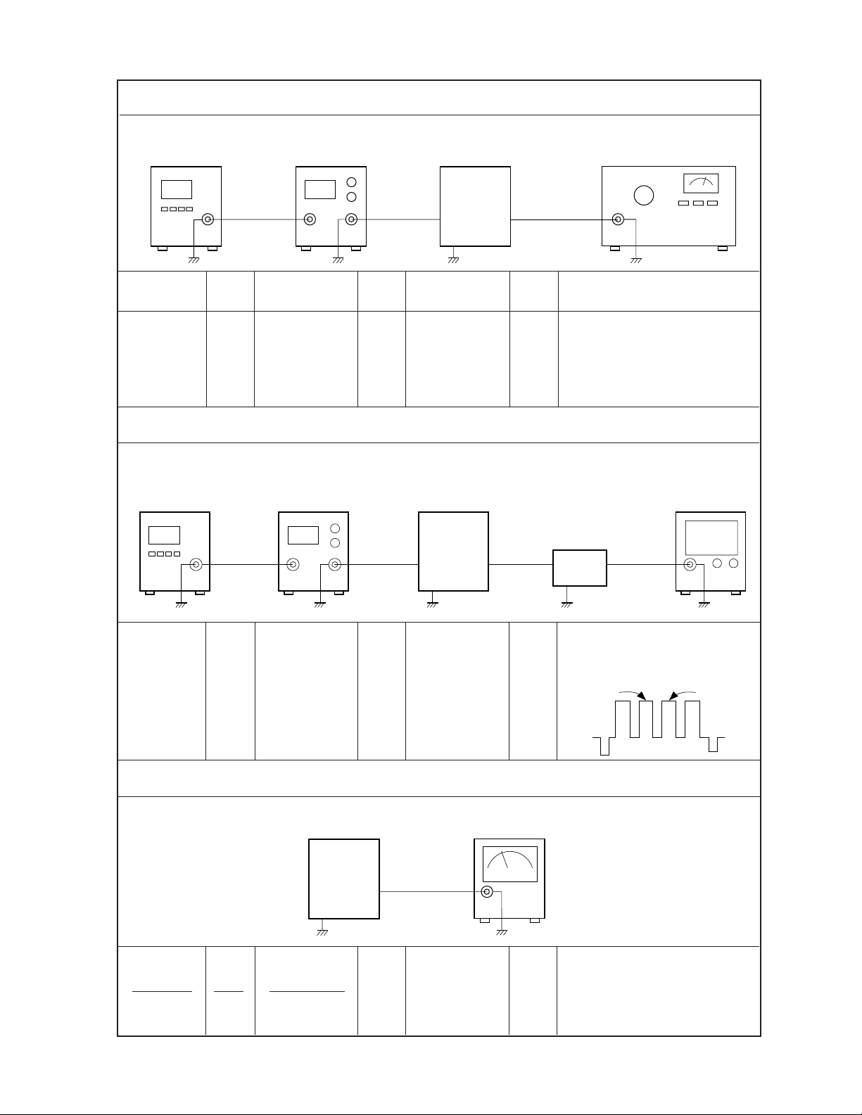
Linear PCB
Pad IF
BU
BS
BV
BM
VHF(L)
0V
20.8V
3.8V
3.8V
VHF(H)
0V
0V
3.8V
3.8V
SCHEMATIC DIAGRAMS AND WAVEFORMS
UHF
3.8V
0V
0V
3.8V
1
2
3
TP3 TP4
TP6
TP2
11
12
4
8
13
7
6
5
TP5
— 19 —
Page 20

PW PCB
10
9
TP1
— 20 —
Page 21

KY PCB
CN700
XXXX
SP+
SP–
KDB
Vcc2
SP600
2803BFB
HP601
CP601
4
3
2
1
CP701
CP702
C702
0.01
SW701
HP602
UP
SKHUPD-T
–
+
0.1
C701
CP700
GND to CHASSIS
R701
4.7K
SW702
SKHUPD-T
DOWN
— 21 —
Page 22

WAVEFORMS
160mV
260mV
63.5µsec 63.5µsec 63.5µsec
1 Q200 Collector
0.3µsec
4 IC300 Pin 23 5 IC300 Pins 10,11,12 6 IC300 Pin 5
2 IC200 Pin 19 3 IC200 Pin 18
700mV
63.5µsec 63.5µsec
3.0V
920mV
1.0V
1.3V
2.5V15V
63.5µsec63.5µsec
7 IC300 Pin 4 8 IC300 Pin 1 9 Q111 Collector
3.6V
2.2V
4.4µsec 140nsec
0 Q111 Base A IC700 Pin 17 B Q806 Base
2.6V
63.5 µsec
4.4µsec
640mV
100µsec
C IC700 Pin 12
— 22 —
Page 23

8-11-10, Nishi-Shinjuku
Shinjuku-ku, Tokyo 160, Japan
Telephone: 03-3347-4926
 Loading...