

Page 1
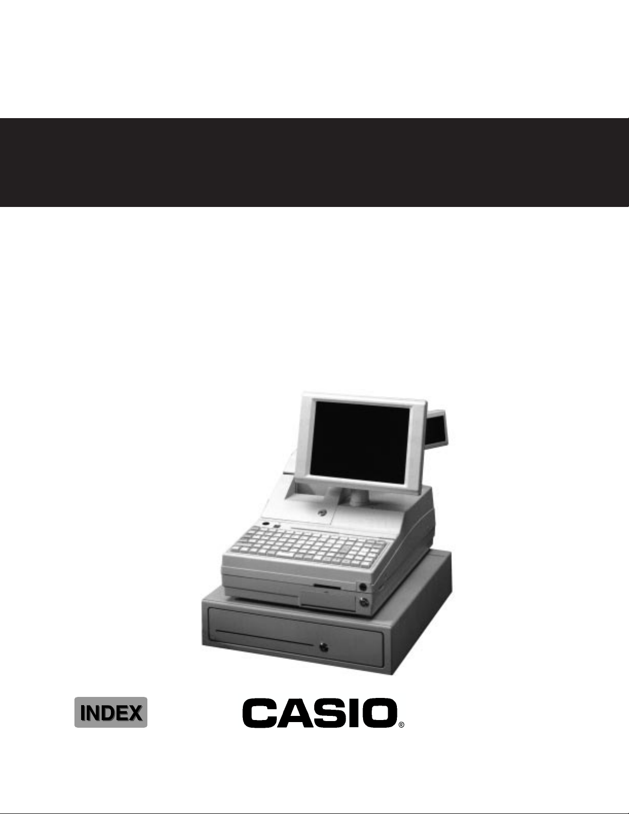
SERVICE MANUAL
REVISE DATE : MAR-98
(without price)
ELECTRONIC CASH REGISTER
SA-5000 (EX-955)
SA-5100 (EX-956)
JUNE 1997
Page 2

CONTENTS
SA-5000/5100 .......................................................................................................Page
1. FEATURES ............................................................................................................. 1
1-1. System Features.............................................................................................. 2
1-2. System Overview............................................................................................. 2
1-3. System Description.......................................................................................... 4
2. SPECIFICATION..................................................................................................... 8
2-1. SA-5000/5100 unit........................................................................................... 7
2-2. SA-5001C/SA-5002M ...................................................................................... 7
2-3. HDD ................................................................................................................. 7
2-4. FDD.................................................................................................................. 7
2-5. MCR (2 track) .................................................................................................. 7
2-6. PRINTER......................................................................................................... 8
3. OPERATION LIST .................................................................................................. 9
4. OPERATION INSTALLATION ................................................................................ 9
4-1. Operator LCD display (SA-5001M, SA-5002C) ............................................... 9
4-2. Adjustment of LCD Dispray ........................................................................... 10
4-3. Customer display (SA-5060N, SA-5061D, SA-5062DH) ............................... 11
4-4. Drawer ........................................................................................................... 14
4-5. Barcode Seanner/Reader (User option) ........................................................ 14
4-6. Ethernet ......................................................................................................... 14
4-7. AC Voltage selection (110/220V Switch)....................................................... 14
5. CIRCUIT EXPLANATION ..................................................................................... 15
5-1. BLOCK DIAGRAM for SA-5000/5100............................................................ 15
5-2. Motherboard block diagram........................................................................... 16
5-3. Motherboard Jumper and Connector position ............................................... 17
5-4. Jumper Settings............................................................................................. 18
5-5. Interface Specifications.................................................................................. 21
5-6. Memory map.................................................................................................. 25
5-7. Serial Port Assignments ................................................................................ 26
5-8. Keycodes....................................................................................................... 27
5-9. Power supply circuit....................................................................................... 28
5-10. Printer control PCB (SA-5000)..................................................................... 29
5-11. Printer control PCB (SA-5100)..................................................................... 30
5-12. Key control PCB ......................................................................................... 32
5-13. MCR control PCB ........................................................................................ 33
6. To open / close the upper case............................................................................. 34
7. RESET OPERATION ............................................................................................ 36
7-1. Hard reset...................................................................................................... 36
7-2. C-MOS reset.................................................................................................. 36
7-3. Memory change............................................................................................. 36
7-4. BIOS Setup.................................................................................................... 37
8.To change the Monochrome to Color system ........................................................ 43
9.DIAGNOSTIC PROGRAM ..................................................................................... 44
10.TROUBLE SHOOTING ........................................................................................ 50
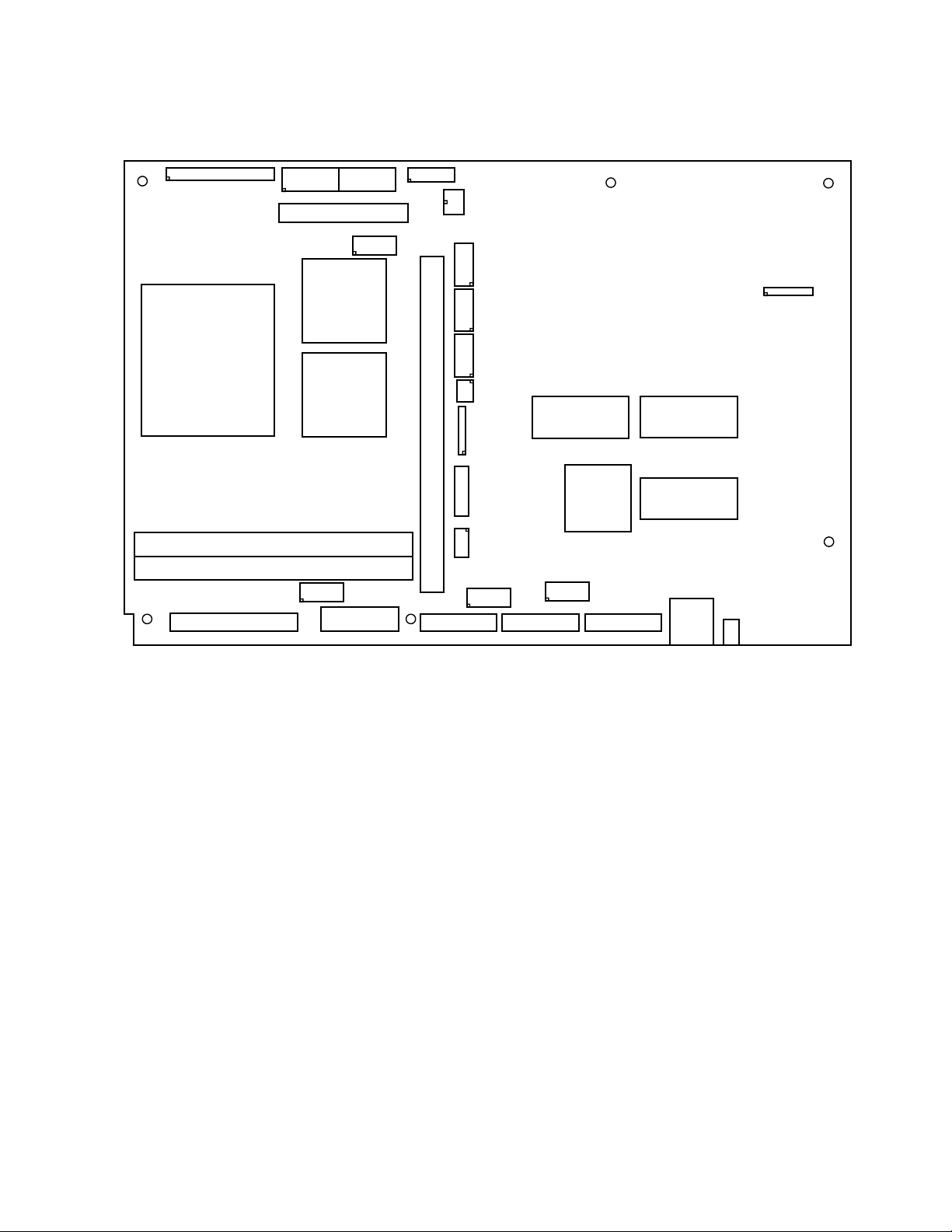
11.PCB LAYOUT ...................................................................................................... 51
12.CIRCUIT DIAGRAM............................................................................................. 54
13. PARTS LIST........................................................................................................ 95
Page 3

1. FEA TURES
1.1 System Features
Feature Standard (specifications) Option
Processor AMD 5X86 133MHz N/A
BIOS AMI N/A
• 4MB DRAM (expandable to 32MB) with
Memory two 72-pin SIMM sockets N/A
• 32KB non-volatile memory (expandable
to 128KB)
Expansion Slots two 16-bit ISA or N/A
one 16-bit ISA and 1 PCI
RS232C Ports 4 Internal and 4 External N/A
(with power output) (2 with 5V or 12V)
Parallel Ports 1 N/A
Floppy Disk 1.44MB N/A
Hard Disk Interface enhanced IDE N/A
3.5"” Hard Disk 1 N/A
• 9.4" Mono VGA LCD or
Operator Display • 10.4" color VGA LCD N/A
with 512KB video memory expandable to 1MB
• 1x11 numeric VFD display or
Customer Display • 2x20 alpha numeric display
(5.5mm or 10.5mm)
Keyboard 90-key POS keyboard N/A
Electronic Keylock 8 positions N/A
Cash Drawer 2 ports with individual sensing N/A
Magnetic Card Reader dual track (track 1 & 2) 1, 2 or 3 tracks ISO
OS Supported MS DOS, Windows
Power Supply 110VAC / 220VAC (165W)
Environment Temperature 5 to 35 degree C N/A
POS Printer • 1-station receipt / journal dot matrix
• 1-station receipt / journal thermal
Packaging recycled textured feel moulded plastic N/A
Software Utilities keyboard remap, BIOS or system setup
Communications Ethernet 10 Base-T N/A
(IEEE 802.3 Ethernet standard)
Dimensions w/o Cash 430mm (W) x 555mm (L) x 340mm (H) N/A
Drawer
Ext PC Keyboard 1
Port/Barcode Reader Port
External VGA Port 1
Note: N/A is short for Not Available.
Table 1.1
— 1 —
Page 4
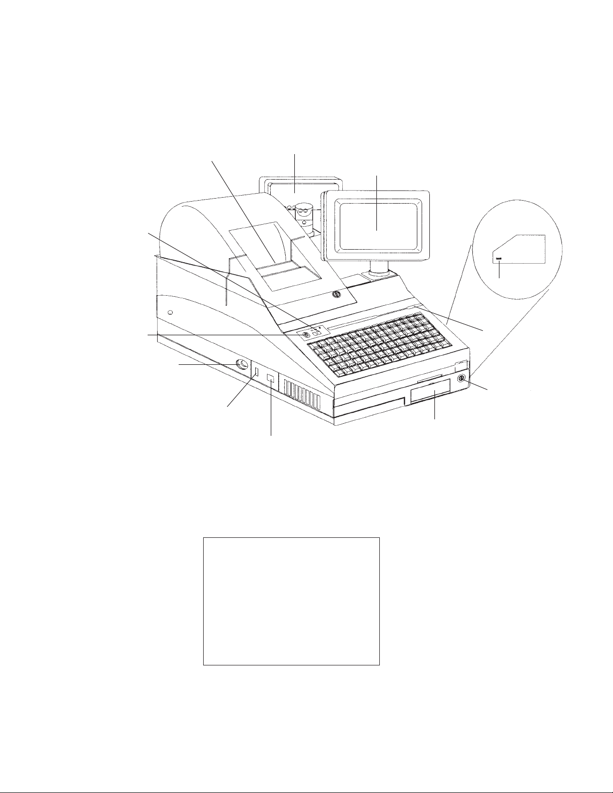
1.2 System Overview
Below are 2 views of the system.
Paper Feed and
Paper Indicator
Electronic Keylock
External Keyboard/
Barcode Scanner Connector
External Keyboard/
Barcode Scanner Selector
Printer
Customer Display
Operator Display
(color LCD or monochrome LCD)
Contrast Adjustment
for LCD Display
Magnetic Stripe
Reader Slot
Floppy Disk Lock
Floppy Cover
ON/OFF Switch
(Main Power)
Figure 1.1 Isometric View
Accessories
1) Journal spooler
2) Roll paper spndle
3) Roll paper
4) Printer ribbon (SA-5000 only)
5) Mode key (3 type x 2 set)
6) Printer cover / FDD cover key
7) Note clip
— 2 —
Page 5
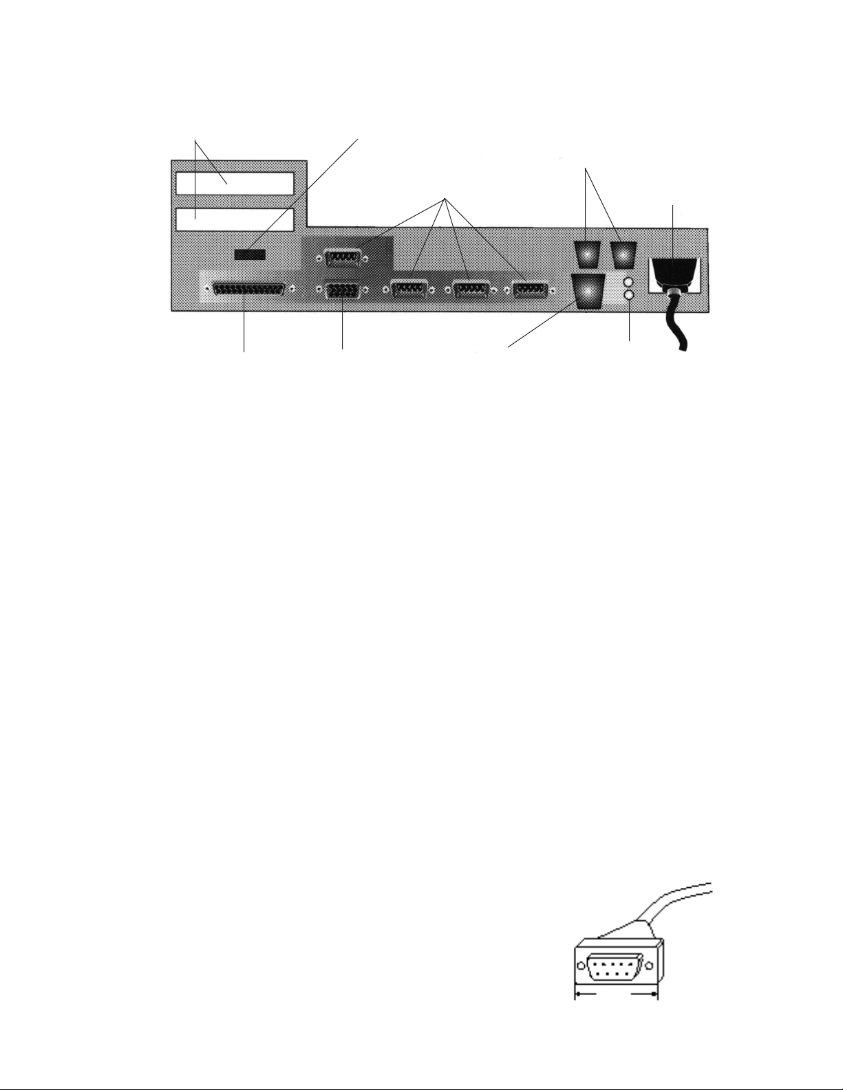
BACK VIEW
Expansion Brackets
Parallel Port
VGA CRT Port
Customer Display
Port
Serial Ports
Ethernet
Cash Drawer Ports
Power Supply
LED Indicator
Connector
Figure 1-2
Figure 1-1 gives an isometric view of the system. On the front, the Floppy Disk Drive cover can be
locked up with a keylock.
The receipt printer is under the printer cover while the Customer Display is behind the Operator
Display which is a LCD display .
On the left side, the Power On/Off switch is hidden by a plastic cover which also hide the External
Input Device slide switch for either PC AT keyboard or Bar Code Scanner. The connection port is
hidden by a rubber plug. On the right side, there is the contrast dial knob for the contrast function of
the LCD panel.
Figure 1-2 gives the rear view. With the rear plastic cover removed, the connectors are revealed.
The 25-pin D-Sub connector for the parallel port is on the extreme left while the 3-pin plug for AC
power supply is on the extreme right.
From left to right, the 15-pin D-sub VGA connector for CRT connection, three 9-pin D-sub
connector, 2 RJ-11 connec-tors, which are part of the Printer Controller board, for Cash Drawers
and RJ-45 connector for Ethernet can be seen.
Above the row of these connectors is the 2x5 2mm connector for the Customer Display and another
9-pin D-sub connector for the serial port.
Note: Due to physical construction, there is limitation in
width of the RS-232C connector.
Maximum width is 28.0 mm. Most of ready-made
cables in the market are applicable.
Width
— 3 —
Page 6
1-3. System Description
1-3-1. Motherboard
Memory 2 x 72-pin SIMM sockets.
STD. : 4MB Max. 32MB of DRAM.
Non-Volatile RAM The NVRAM can be used to store transactions and data for backup
purpose. STD : 32KB MAX.: 128KB
Internal Ports Ports for interfacing the internal POS devices reside on the
motherboard. The interfaces are for the POS printer, operator and
2x20 customer displays and the Keyboard Controller Board.
The Keyboard controller Board contains the interfaces for the
Magnet Stripe Reader and the 1x11 numeric customer display.
External Ports Ports for interfacing the external devices reside on the motherboard
and are accessible through the rear panel.
1 x Parallel port
4 x RS232C ports - two of which provide +5V and +12V,
2 x Cash drawer ports with individual sensor
1 x VGA CRT port
1 x Ethernet 10 base-T port
1 x external keyboard or a Bar Code Reader port
Expansion Slots 2 x ISA slots or 1 x ISA slot and 1 x PCI slot
The length of add-on cards should not exceed 200 mm.
VGA Video System The video controller is on the motherboard to support VGA LCD
displays.
9.5” monochrome LCDor 10.4” Color DSTN LCD
The LCD panel can be rotated, tilted or slid horizontally.
The SA-5000 mounts the monochrome video BIOS ROM and the
SA-5100 mounts the colour video BIOS ROM as standard.
For flexible system configuration, monochrome or colour LCD
display is available for both models by switching video BIOS ROM
and jumper setting on the motherboard (JP31, JP46).
The video system also supports VGA CRT monitor.
Automatic frequency detection type CRT is recommended.
(Horizontal frequency is about 25KHz)
BIOS BIOS : AMI (American Megatrends Incorporated)
The following is a list of modifications which were made to the
standard BIOS.
1. System Setup
2. Chipset Setup
3. Support for 8 serial ports
4. System Self Test
5. Power Restore/Backup
— 4 —
Page 7
1-3-2. Customer Displays
The system offers two choices of customer display.
Alphanumeric VFD The character height : 10.5mm (SA-5062DH) or 5.5mm (SA-5061D).
2 X 20 The display has a RS232C serial interface and is connected to the
9-pin D-sub connector on the rear bracket at the rear of the housing.
Numeric VFD Thecharacter height is 11 mm (SA-5060N).
1 x 11 The display has two connectors to be connected to the connectors on the
keyboard controller board inside of the unit, underneath the keyboard.
Open one of ISA expansion slot on the rear bracket and thread the cables
into the unit.
1-3-3. Operator Displays
SA-5002C VGA color LCD flat panel display
SA-5001M VGA monochrome LCD flat panel display
1-3-4. Keyboard
The keyboard contains 90 keys which can be re-labelled to support double wide, double high and
quad keys.
The scancodes are programmable. An alternative flat membrane water resistance keyboard with
120 keys is available.
1-3-5. Manager’s Electronic Keylock
The system contains a 8-position manager’s keylock.
1-3-6. Magnetic Stripe Reader
The MSR input is similar to a keyboard input.
2 tracks (track 1 and 2) is standard, 3 tracks (track 1 , 2 and 3) is optional.
1-3-7. Printers
The system housing is designed to accommodate different printer mechanisms with different covers
as indicated in the table below.
Model Type of Printer Printer Mechanism
SA-5000 Single Station Dot Matrix Citizen-614 with validation
SA-5100 Single Station Thermal Citizen-380
— 5 —
Page 8

1-3-8. Cash Drawers
The system can support up to two cash drawers.
1-3-9. Ethernet
The system provides a 10Mbps connectivity to a Local Area Network complying with the IEEE802.3
Ethernet standard.
The Ethernet controller adopts a Bus-Master approach for maximum throughput on the ISA bus.
Driver information need to be specified.
1-3-10. Floppy Disk Drive
The system supports one 1.44 MB floppy disk drive which can be locked up with a mechanical
keylock.
1-3-11. Hard Disk Drive
The system supports up to 2 E-IDE hard disk drives.
Standard : 1 HDD mounted.
— 6 —
Page 9

2. SPECIFICA TIONS
2-1. SA-5000 / 5100 unit
Environment and Safety Specifications
Specifications
Operating Temperature 5˚C — 35˚C
Operating Humidity 20% to 90% Non Cond. RH
Storage Temperature -10˚C — 80˚C
EMI FCC Class A
CE Mark
Safety & ESD cUL1950, GS
CE Mark
Power Supply 110VAC, 60Hz, 165W
220V AC, 50Hz, 165W
2-2. SA-5001C / SA-5002M (Operator LCD Display)
Model LCD Name LCD Life time Remark
SA-5001M LM64183P 10,000 hours or more Monochrome
SA-5002C LM64C55 10,000 hours or more Color
Note : Life time conditions
Operating tempurature : 25 ±5°C (Monochrome), 25 ±1°C (Color)
Brightness value : Became 50% of the initial value
2-3. HDD
Model MTBF
ST3850A 300,000 hours or 40,000 contacts
2-4. FDD
Model MTBF Device life
MF355F-3 80,000 hours 5 years or 20,000 hours
2-5. MCR (2 track)
Model MTBF
ZU-M1241S1 300,000 pass
— 7 —
Page 10
2-6. Printer
SA-5000
Printer model DP-614
Printing specification Print method : Impact dot matrix
Print direction : Bi-directional
Printing speed : 3 lines / sec.
Dot number of width : 360 dots / line (includ half dot)
Number of columns : 40 columns
Character dots : 7 dots x 9 dots
Character spacing : 2 dots
Paper feed Paper feed method : Friction feed
Line spacing : 1/6 inch (4.23mm)
Line speed : Fast feed : 18 lines / sec.
Normal feed : 9 lines / sec.
Paper Paper width : 76 ± 0.5mm
Paper diameter : Less than 80mm
Paper type : Normal and no-carbonic
Paper thickness : Nomal paper : 0.06 - 0.09 mm
Copy paper : 0.05 - 0.08 mm combination (No-cabonic)
Original 1 + copy 1 : Less than 0.14mm
Reliability MCBF : 4,000,000 lines
Head life : 80,000,000 characters
Ink ribbon life : 2,600,000 characters (Black)
SA-5100
Printer model LT-380
Printing specification Print method : Thermal line dot method
Total number of dots : 576 dots / line
Dot density : 8 dots / mm
Printing width : 72mm
Printing speed : Max. 500 dots / sec.
Character column numbers and dots :
Dots of font Column numbers
8 x 16 72
16 x 16 36
12 x 24 48
24 x 24 24
Paper feed Low speed : 250 dots line / sec.
High speed : 500 dots line / sec.
Paper Paper width : 80mm ( +0 , -1)
Paper type : Thermal paper
Reliability Head life : At least 50,000,000 pulses (printing rate : 12.5%)
or 30 km
— 8 —
Page 11
3. OPTION LIST
Device Product Name Description
Operator display SA-5001M 9.4 inch Monochrome LCD display
SA-5002C 10.4 inch Color LCD display
Customer display SA-5060N 1x11 Numeric display
SA-5061D 2x20 Alpha display (5.5mm hight )
SA-5062DH 2x20 Alpha display (10.5mm hight)
Second Drawer M-sized drawer with open sensor
Magnetic Card Reader SA-5040MCR 3 track reader
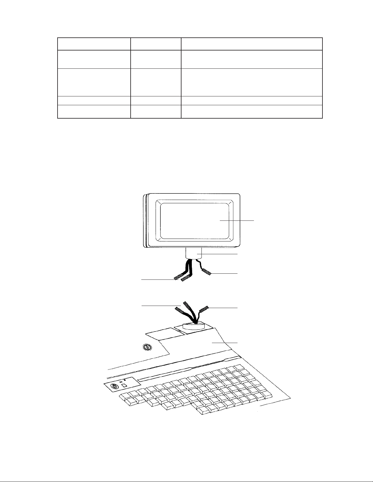
4. OPTION INSTALLATION
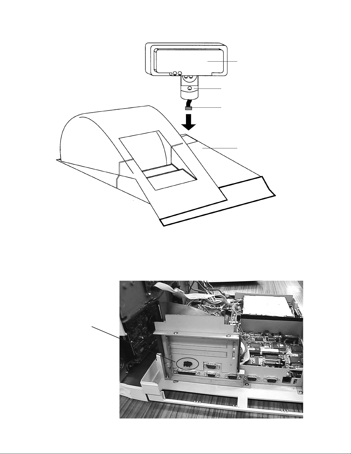
4-1. Operator LCD display (SA-5001M, SA-5002C)
Note : Make sure that the power switch is turned off.
Signal Cables
Mono : one cable
(
Colour : two cable
Signal Cables
LCD Display
(Top Assembly)
Neck
Power Cable
Power Cable
System Assembly
Installing LCD Display to System
— 9 —
Page 12
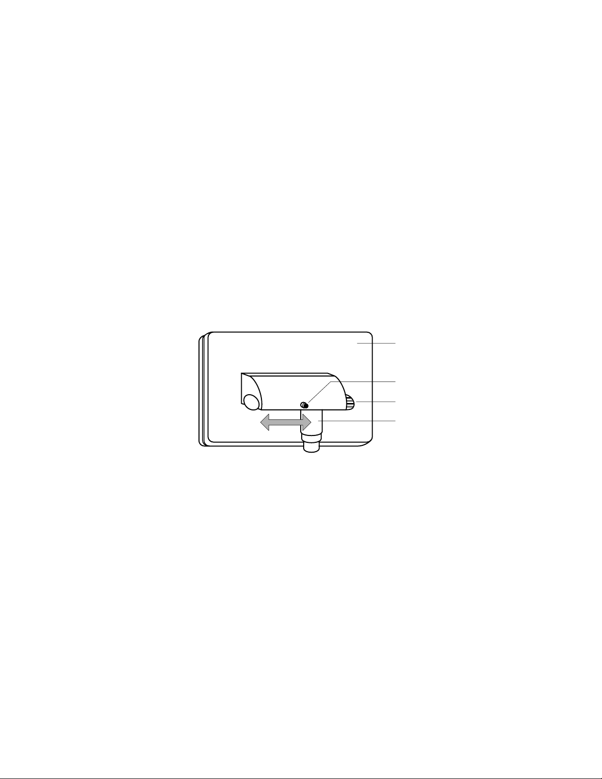
sliding position
along the bar
LCD Display
Tightening Knob
Sliding Bar
Neek
1. Connect the power cable protruding from the neck of the top assembly to the power cable of the
system assembly.
2. Then connect the signal cables protruding from the neck of the top assembly to the signal cables of
the system assembly.
3. Finally, position the display unit such that the neck sits comfortably on the system assembly.
Once the LCD panel is properly installed, it can no longer be detached from the system assembly.
4-2. Adjustment of LCD Display
The operator display can be easily adjusted for the operators viewing comfort.
The display unit can be tilted, swivelled and moved to the right or left.
The neck of the unit is built such that it allows tilting at different angles.
To move the display to the left or right, simply loosen the tightening knob situated at the back of
the unit.
Then move the display along the sliding bar to the desired position before tightening the knob again.
To swivel, simply lift up the display and rotate to desired position.
— 10 —
Page 13
4-3. Customer display (SA-5060N, SA-5061D, SA-5062DH)
Take top cover on upper case and screw
pole kit.
Thread display cable(s) into case
Customer Display
(T op Assembly)
Neck
10-pin Ribbon Connector
System Assembly
Installing Customer Display to System
1. Alphanumeric 2x20 type (SA-5061D, SA-5052DH)
Connect the 10-pin ribbon cable to the 10-pin connecter on the rear panel.
Connect here.
— 11 —
Page 14
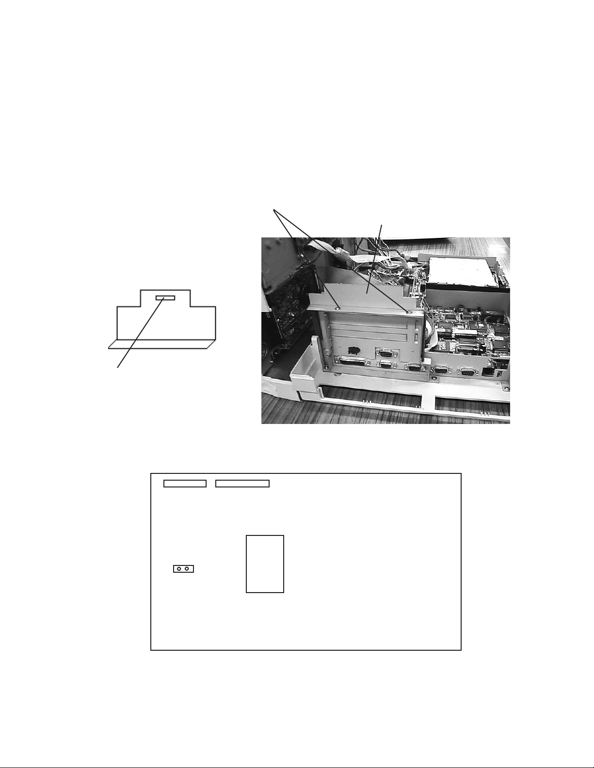
2. Numeric 1x11 type (SA-5060N)
1. Connect 2 pcs of expansion cable which is the SA-5060N carton box to SA-5060N.
2. Open the upper case and release the screw to fixing the bracket.
3. Change the bracket which is in the SA-5060N carton box and insert the cable to the hole.
4. Then, connect 2 pcs of expansion cable to the connector CN1,CN2 on the keyboard controll PCB.
5. Make short the jumper JP1 on the keyboard controll PCB using short pin which is mounted PCB.
JP1 condition : Open : Not mounted SA-5060N Default
Short : Mounted SA-5060N
6. Close the upper case.
Release these screws.
Bracket
Bracket in the carton box
Insert the cable to this hole.
CN1
JP1
CN2
ROM
Printer controll PCB
— 12 —
Page 15
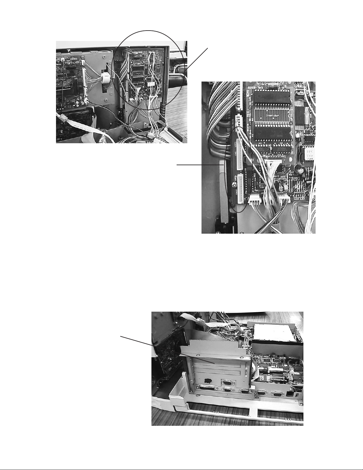
PCB LOCATION
Connect 2 pcs of cable here.
Printer controll PCB
CONNECTOR LOCA TION
Note : In case the SA-5060N has no replacement bracket in the carton, please remove the cover
for expansion board.
Then, insert the cable this hole.
Remove this cover and insert
2 pcs of cable here.
— 13 —
Page 16
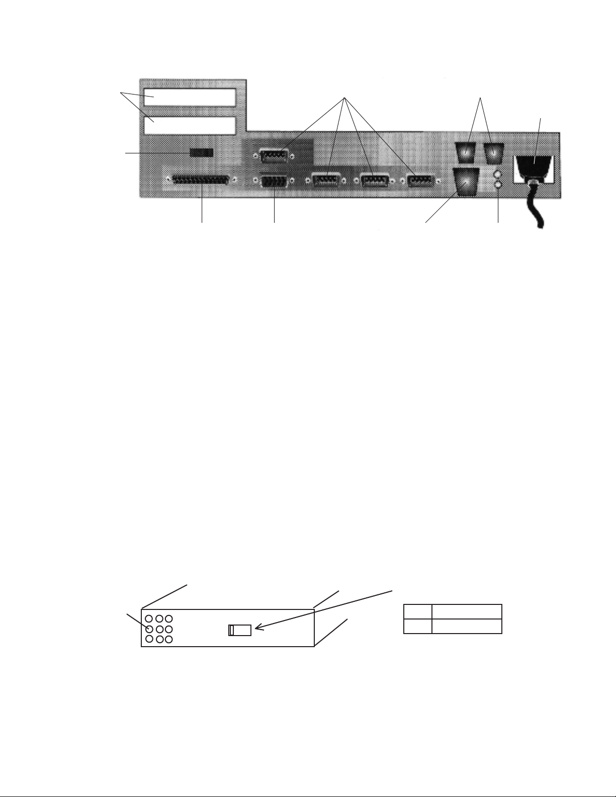
4-4. Drawer
Expansion
Brackets
Customer
Display Port
Parallel Port
VGA CRT port
Serial ports
Ethernet
Connector
SYSTEM REAR VIEW
SA-5000/5100 have two cash drawer ports located at the rear of the system.
A maximum of two cash drawers can be connected to the system through these ports.
Note: Type of connector for the Ethernet port is similar to connector for the cash drawer.
Please confirm location carefully and connect the cash drawer.
4-5. Barcode Scanner/Reader (User option)
Drawer ports
Power supply
Indicator
Connect the barcode scanner/reader 9-pin D-shell connector to the barcode scanner connector
located at the left hand side of the terminal.
The selector next to the connector should be set to “ S “ position.
Ensure the barcode scanner/reader is the AT-keyboard connector type.
4-6. Ethernet
The connector used for Ethernet LAN is RJ45.
4-7. AC Voltage selection (110/220V Switch)
Important!
The power supply unit has a voltage selector and it is possible to adjust the input voltage level.
To adjust the voltage lebel, open the upper case and slide the selector to AC voltage position.
Power supply unit
Air hole
115
Selector
115 100V - 120V
230 220V - 240V
Connect AC power cord to the power supply connector securely.
L angled connector type AC cord is recommended to close back case cover securely.
Power-Up
The system is powered up upon switching on the On/off button.
The system will then perform the Power-On-Self-Test (POST).
After the POST is completed, the system will boot from the hard disk or the floppy disk.
— 14 —
Page 17
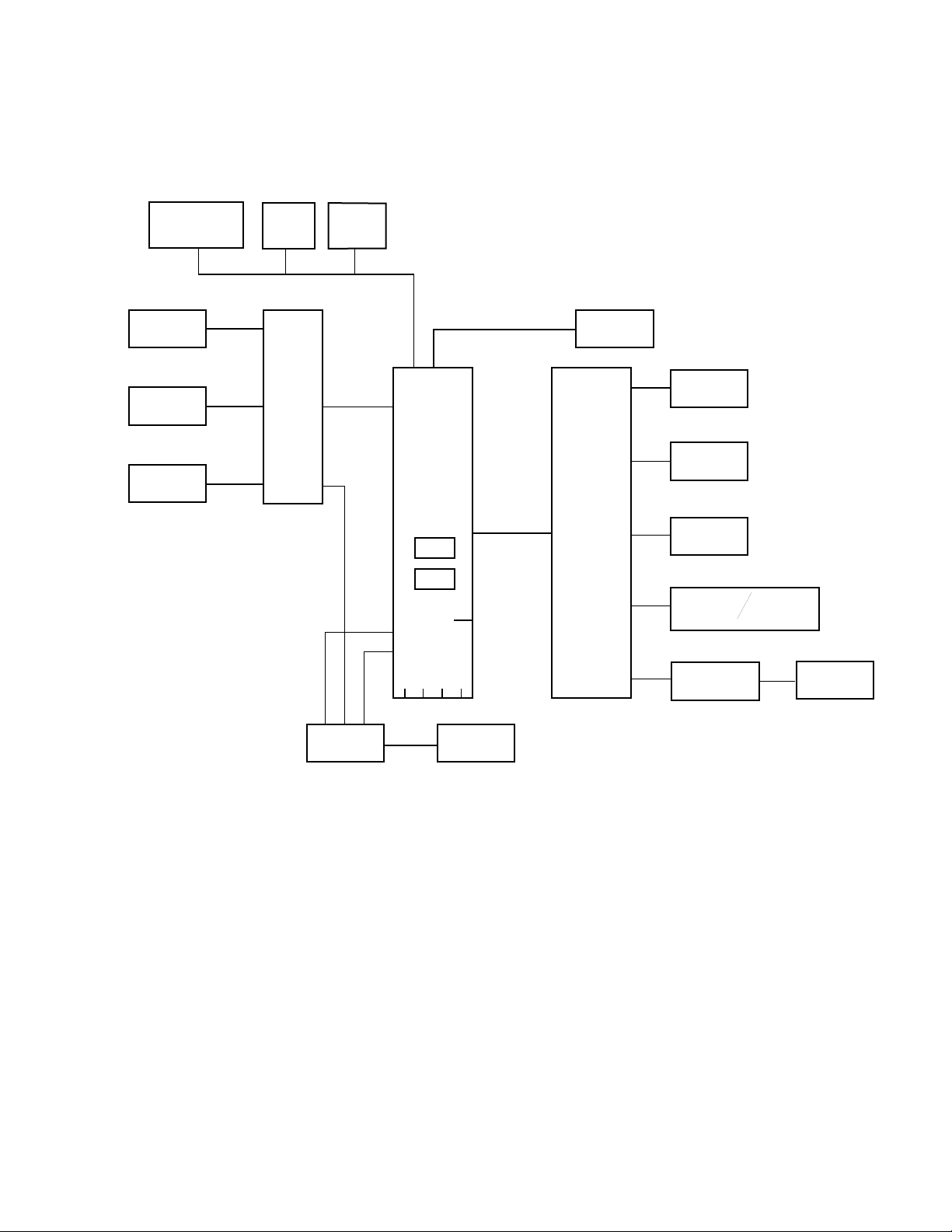
5. CIRCUIT EXPLANATION
5-1. BLOCK DIAGRAM for SA-5000/5100
∗
Mono / Color
LCD DISPLAY
PRINTER
∗
DRAWER 1
∗
DRAWER 2
Parallel
port
PRINTER
BOARD
Ethernet
10 baseT
RS232C 3
RS232C 1
MOTHERBOARD
ISA 2
KEYBOARD
INTERFACE
ISA 1
LPT 1
∗CUSTOMER
DISPLAY
2 X 20
KEYBOARD
CONTROLLER
∗CUSTOMER
DISPLAY
1 X 11
POS
KEYBOARD
MANAGER
LOCK
∗
BAR CODE
READER
∗
PC
KEYBOARD
MCR
CONTROLLER
* : OPTION
POWER
SUPPLY
RS232C 2
POWER
OFF
SENSOR
RS232C 4
RS232C 7
RS232C 8
SLIDE
SWITCH
AC110/230V
Memory socket : 2 x 72 pin SIMM
Expansion socket :2 x ISA slot ( Card should be less than 200mm ) or
1 x ISA slot and 1 x PCI slot
RS232C Port : RS232C port In the above fugure is mentioned internal port number.
It is possible to supply the power (+5V, +12V) on port 2 and 4.
MAGANETIC
CARD
READER
— 15 —
Page 18
CPU
586
ROM
ISA
RTC
KB
M1487
IBC
DRAM
M1489
CMP
PCI
HDD
CD-ROM
M1489 / M1487 System Block Diagram
IDE
SA
for serviceing porpose
No room to mounting
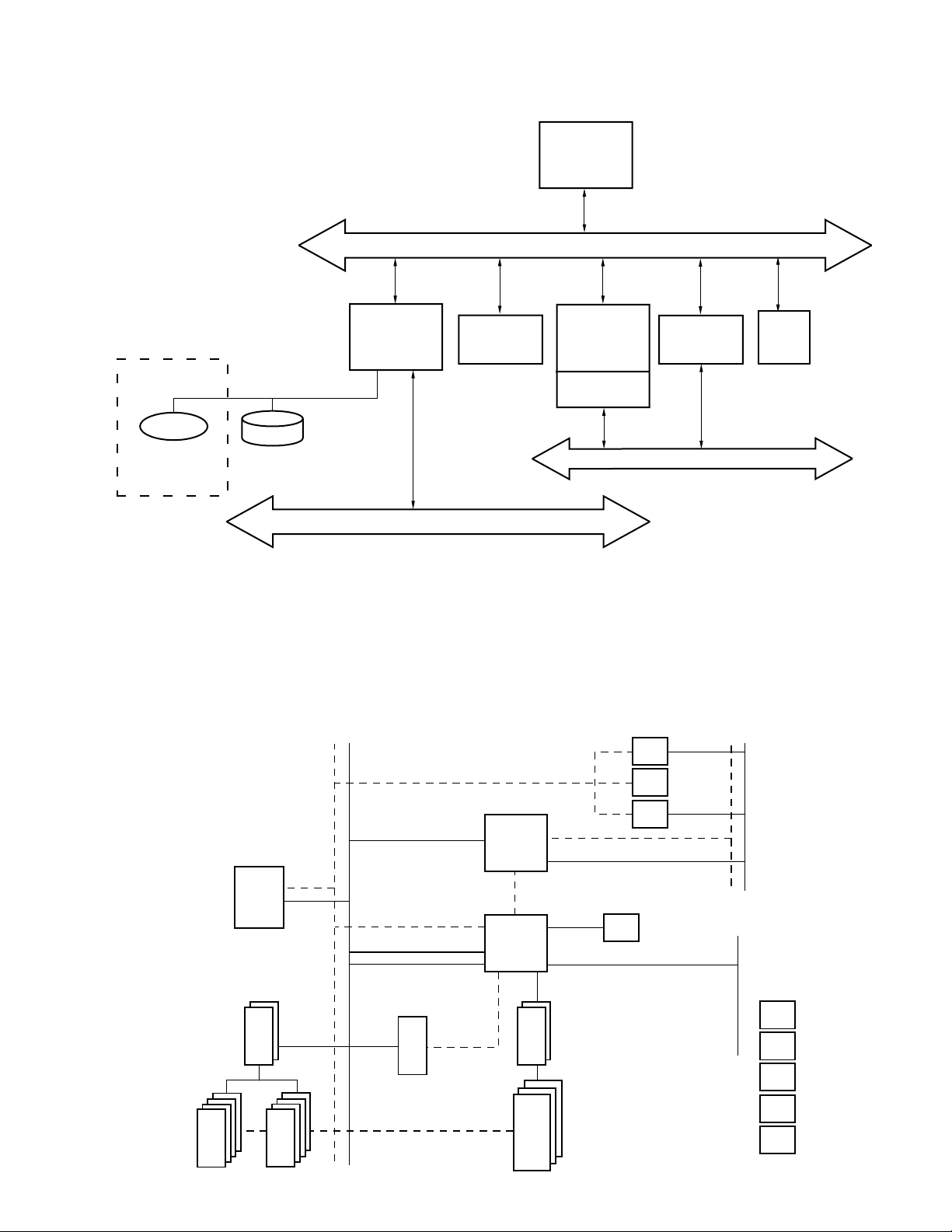
5-2. Motherboard block diagram
M1489CMP : Controls cache memory and PCI bus
M1487IBC : ISA bus controller
RTC : Real time clock (Dallas DS12887A )
CD ROM : CD ROM is used for serviceing purpose. There is no room to mount the CD-ROM.
SRAM
X4
CPU
2 bank
optional
F244
X2
SRAM
X4
HOST
GD GA
GA(9:2)
GA(17:2)
GA(26:2)
GA31
TAG
SRAM
TAG
IBC
M1487
LINK_BUS
CMP
M1489
TAG
SRAM
DRAM
4
BANK
RASJ
MA
XD
driving
optional
IDC
ROM
RTC
KBC
optional
optional
ISA
SD SA
PCI
7404
7408
7406
14069
CLKGEN
osc,reset
optional
DRAM parity
optional
KBC
optional
RTC
optional
— 16 —
Page 19
5-3. Motherboard Jumper and Connector position
J1
FLOPPY DISK DRIVE
CPU
MEMORY SOCET
J11 PARALLEL
PS1
POWER SUPPLY
PS2
J2
HARD DISK DRIVE
PRINTER
J3
ALI
ALI
J17 VGA
J12 VGA
POWER SUPPLY
PS3
TO KEYBOARD
BATTERY
PS4
FOR GUS
CUSTOMER
J4
DISPLAY
J5
J6
KEYBAORD
J7
CONTROLLER
MONO LCD
J10
23 BUS SOCKET
J
COLOR LCD
J9
LCD
J8
COMSTRAST
EXT SERIAL 1
SYSTEM BIOS
J13
J14
EXT SERIAL 2 EXT SERIAL 3
J15
J25
J16
EXT SERIAL 4
VGA BIOS
J18
J43
LED1
— 17 —
Page 20
5-4. Jumper Settings
Change the jumper settings for each type of CPU used according to the table below.
CPU TYPE SETTING
JP 486DX F P24C P24D P24T AMD+ AMD 5x86
8 2-3 2-3 2-3 1-2 2-3 2-3
9 Fit F Fit F Fit F Fit F Fit Fit
12 1-2 1-2 2-3 2-3 1-2 1-2
19 N-F N-F 2-3 N-F 2-3 2-3
23 N-F Fit Fit Fit Fit Fit
36 1-2 3-4 3-4 3-4 3-4 1-2
37 3-4 3-4 3-4 3-4 3-4 3-4
38 3-4 3-4 3-4 3-4 3-4 3-4
39 N-F N-F 5-6 N-F 1-3, 5-6 1-3, 5-6
:default
Fit = Fitted / N-F = Not Fitted / Default setting is marked by an AT-sign F /
JP9 Fitted for Write Thru, Not Fitted for Write Back / JP39 1-3 Fitted for 133 MHz
Select the clock frequencies according to the CPU speed according to the table below.
CPU CLOCK SETTING
JP25 JP26 JP27 CPU CLOCK CPU CLOCK/2
(S2) (S1) (S0) (MHz) (MHz)
Fit Fit Fit 33.3 16.65
Fit Fit 80 40
Fit Fit 66.67 33.3
Fit 50 25
Fit Fit 40 20
Fit 60 30
Fit 25 12.5
33.3 F
16.65 F
:default
— 18 —
Page 21
JP 1-2 2-3 Description
1 for DS12887 for DS12887A CMOS Reset (do not insert)
3 for GUS for Mistoffelees Power Switch Status Detection
4 INTEL CPU * TI CPU Backup Status
5 +5V Ring Indicator Int. Serial Port #3 Pin 9
10 +12V Carrier Detect Int. Serial Port #3 Pin 1
11 3.45V 3.3V 3.3V/3.45V CPU Volt Selection
14 32KB 16K
15 DS1650Y (512K) DS1230Y/32K NVRAM Type Selection
DS1225Y/8K Not fitted/Open for DS1245Y/128K
DS1220Y/2K
21 300H 100H Base I/O Addr Sel. for Serial Port
28 PCI Clk=CPU Clk PCI Clk=CPU Clk/2 PCI Clock Selection
30 -VEE +VEE
31 Color LCD Panel Monochr. LCD Panel VCON(Contrast Volt) Selection
32 +5V Ring Indicator Ext. Serial Port #2 Pin 9
35 +12V Carrier Detect Ext. Serial Port #2 Pin 1
34 +5V Ring Indicator Ext. Serial Port #1 Pin 9
33 +12V Carrier Detect Ext. Serial Port #1 Pin 1
F NVRAM Page Size Selection
VEE Selection: Sharp LM64183P
:default
JP Open/Not fitted Close/Fitted Description
2 default Reset Momentarily
6 default Bypass Speaker Speaker Connection
7 3.3V/3.45V CPU 5V CPU
16 PCI Clk=CPU Clk PCI Clk=CPU Clk/2
40 Disable Enable Video Test Mode Selection
41 Disable Enable 2 X CPU Clk Select for VGA
42 Disable Enable Ethernet Boot ROM Selection
:default
JP Mono LCD Colour LCD
46 1-2 2-3
47 1-2 1-2
— 19 —
Page 22

The table below shows a summary of all jumper description.
JP PINS WHAT FOR
1 3 CMOS Reset (not to be inserted)
2 2 System Reset (not to be inserted)
3 3 Power Switch Status Detection
4 3 Backup Status
5 3 Internal Serial Port #3 - pin 1 & pin 9 selection (5V)
6 2 Speaker Bypass
7 2 CPU V oltage Selection
8 3 CPU Type Selection
9 2 CPU Type Setting - AMD or Others
10 3 Internal Serial Port #3 - pin 1 & pin 9 selection (12V)
11 3 3.3V/3.45V CPU Voltage Selection
12 3 CPU Type Selection
13 X
14 3 NVRAM Page Size Selection
15 3 NVRAM Type Selection
16 2 PCI Clock Selection
17 X
18 X
19 3 CPU Type Selection
20 X
21 3 Base I/O Address Selection for Serial Port Decoding
22 X
23 3 CPU Type Selection
24 3 Non-volatile DRAM on SIMM
25 2 CPU Clock Setting
26 2 CPU Clock Setting
27 2 CPU Clock Setting
28 3 PCI Clock Selection
29 3 Non-volatile DRAM on SIMM
30 3 VEE Selection for Mono LCD Panel
31 3 VCON (Contrast Voltage for LCD panel) Selection
32 3 External Serial Port #2 - pin 1 & pin 9 Selection (5V)
33 3 External Serial Port #1 - pin 1 & pin 9 Selection (12V)
34 3 External Serial Port #1 - pin 1 & pin 9 Selection (5V)
35 3 External Serial Port #2 - pin 1 & pin 9 Selection (12V)
36 6 CPU Type Selection
37 6 CPU Type Selection
38 6 CPU Type Selection
39 6 CPU Type Selection
40 2 Video Test Mode Selection
41 2 2 X CPU Clock Select for VGA
42 2 Ethernet Boot ROM Selection
43 8 Lattice PLD - not to be used
44 3 SIMM 1 Selection - Volatile or Non-volatile
45 3 SIMM 2 Selection - Volatile or Non-volatile
46 3 3.45V/5V Selection for VGA for Color/Mono LCD
47 3 3.45V/5V Selection for Color/Mono LCD
— 20 —
Page 23
5-5. Interface Specifications
J Connector J Connector
1 FDD 16 Serial Port w/o V oltage Supply
2 HDD 17 External VGA
3 Printer 18 Non-existent
4 Serial Port w/ Voltage Supply 19 Non-existent
5 Serial Port w/ Voltage Supply 20 Non-existent
6 Serial Port w/ Voltage Supply 21 Non-existent
7 Keyboard Interface 22 Non-existent
8 Contrast Voltage Adjustment 23 Non-existent
9 Color LCD Display 24 Non-existent
10 Monochrome LCD Display 25 Serial Port for Smart Card (see J3)
11 Parallel Port 26 Internal VGA Port (see J12)
12 VGA Port 27 Non-existent
13 Serial Port w/ Optional Voltage Supply 28 Non-existent
14 Serial Port w/ Optional Voltage Supply 29 Non-existent
15 Serial Port w/o Voltage Supply 30 Non-existent
[Summary of all the Ports]
5-5-1. Power Supply Connectors
PS1 Power Supply Connector PS3 UPS Connector
1 Power Good 1 Gnd
2 +5V 2 +10V
3 +12V 3 Enable Backlight
4 -12V 4 Power Fail
5 Gnd 5 Power Switch On/Off
6 Gnd 6 UPS Off
7 Gnd
8 Gnd
9 -5V
10 +5V
11 +5V
12 +5V
[Power Supply Connection]
The UPS connection is used only for battery-backup system.
— 21 —
Page 24

5-5-2. LCD VGA Ports
Pin J9 - Color LCD Display J10 - Monochr. LCD Display
1 DL4 - Display Data Signal Scan Start-up Signal
2 Gnd Input Data Latch
3 DL5 Data Input Clock
4 Scan Start-up Signal +5V
5 DL6 +5V
6 Input Data Latch Gnd
7 DL7 VEE - Power supply for LCD
8 Gnd DU0
9 Gnd DU1
10 Data Input Clock DU2
11 DL0 DU3
12 Contrast Adjust Voltage DL0
13 DL1 DL1
14 +5V DL2
15 Gnd DL3
16 +5V
17 DL2
18 +5V
19 DL3
20 Gnd
21 DU3 - Display Data Signal
22 DU4
23 DU2
24 DU5
25 DU1
26 Gnd
27 DU0
28 DU6
29 Gnd
30 DU7
[LCD Ports]
— 22 —
Page 25

5-5-3. VGA Ports
Pin J12 - VGA (D-Sub 15pin) J26 - Header 10pin
1 Red
2 Green
3 Blue
4 Gnd
5 Gnd
6 Gnd
7 Gnd
8 Gnd
9 HSync
10 VSync
11
12
13
14
15
[VGA Connection]
5-5-4. Serial Ports
Serial Port Default Peripheral Location on M/B +12V, +5V
#1 Customer Display J4 Default
#2 J5 Default
#3 POS Printer J3 Selectable
#4 J6 Default
#5 User-defined J14 & J25 Selectable (0.5A Fuses)
#6 User-defined J13 Selectable (0.5A Fuses)
#7 User-defined J15 Nil
#8 User-defined J16 Nil
[Overview of Serial Ports]
Pin J3 J4 J5 J6
1 +12V/CD +12V +12V +12V
2 Rxd Rxd Rxd Rxd
3 Txd Txd Txd Txd
4 DTR DTR DTR DTR
5 Gnd Gnd Gnd Gnd
6 DSR DSR DSR DSR
7 RTS RTS RTS R TS
8 CTS CTS CTS CTS
9 +5V/RI +5V +5V +5V
[4 of the 8 Serial Ports]
— 23 —
Page 26
Ext. Port #1 Ext. Port #2 Ext. Port #3 Ext. Port #4
Pin J13 J14 J15 J16
1 +12V/CD +12V/CD CD CD
2 Rxd Rxd Rxd Rxd
3 Txd Txd Txd Txd
4 DTR DTR DTR DTR
5 Gnd Gnd Gnd Gnd
6 DSR DSR DSR DSR
7 RTS RTS RTS RTS
8 CTS CTS CTS CTS
9 +5V/RI +5V/RI RI RI
[Another 4 of the Serial Ports]
5-5-5. Ethernet Port
The connector used conforms to the industry-standard RJ-45. Refer to the relevant documents.
5-5-6. Drawer Port
Pin Number Signal Name Signal Direction
1FG NA
2 Drawer kick drive A Output
3 Drawer open/close Input
4 +24V NA
5 Drawer kick drive B NA
6SG NA
[Cash Drawer]
— 24 —
Page 27
5-6. Memory map
The memory system is that of the IBM AT PC-compatible.
The size of the system memory depends on the size of the SIMM fitted. See the figure below.
00000
640KB
CONVENTIONAL
MEMORY
A0000
VIDEO BUFFER &
EXPANSION AREA
D8000
E0000
F0000
FFFFF
32K NVRAM
ROM BASED
SYSTEM UTILITIES
BIOS
— 25 —
Page 28
5-7. Serial Port Assignments
For convenience, the serial port table is reproduced here.
The serial ports for the optional operator display and the 2x20 customer display are controlled by
ACER M5105-A4 controller chip.
These ports support only IRQ3 and IRQ4 and can go up to 56Kbps.
No. Location Default Device Selectable Selectable Legend Default
Add Setting IRQ Addr/IRQ
#1 Internal Customer Display 02E8, 02F8 3 - 03F8 / 4
03E8, 03F8 4
#2 External User-defined as below as below Ext 1 02F8 / 3
#3 Internal Printer 02E8, 02F8, 03E8, 3, 4, 10, 11, 12 - 03E8 / 10
03F8, 3220, 3228, & 15
4220 & 4228
#4 External User-defined as above as above Ext 2 02E8 / 11
#5 Internal Not used - DIS / DIS
#6 Internal Not used - DIS / DIS
#7 External User-defined as above as above Ext 3 4220 / 12
#8 External User-defined as above as above Ext 4 4228 / 15
: default
To change the default setting, the procedure for changing the setting must be followed.
This is shown in BIOS setup section.
To change the setting, disable all address and IRQ of all serial ports.
Then change from serial port #1.
— 26 —
Page 29
5-8. Keycodes
POS KEYBOARD NUMBER
120 112 104 96 88 80 72 64 56 48 40 32 24 16 0
123 115 107 99 91 83 75 67 59 51 43 35 27 19 3
124 116 108 100 92 84 76 68 60 52 44 36 28 20 4
125 117 109 101 93 85 77 69 61 53 45 37 29 21 13
126 118 110 102 94 86 78 70 62 54 46 38 30 22 14
127 119 111 103 95 82 74 66 58 50 41 33 25 17 9
Key code
ESC F1 F2 F3 F4 F5 F6 F7 F8 F9 F10 F11 F12 Insert
~!@#$%^&*()
‘ 1 2 3 4 5 6 7 8 9 0 = Down
TAB Q E W R T Y U I O P Enter 7 8 9
CAPS
LOCK -
Shift Shift Z X C V B N M
“:{}
‘;[] /
ASDFGHJKL
<>
,.
ALT Space Space ALT CTRL
?
BKSP
_
Enter 4 5 6
^
<-
v
+
Delete
123
|
|
-> 0
Keyboard layout
Page
Up
Page
|
\
— 27 —
Page 30
+
+
+
+
+
+ +
+ +
+
+
+ +
+
+ +
+
+
AC L
AC N
FG
16 15 14 13 12
L1
F1
TR1
R14A
L2
A
C
D1
R11
R24
R17
C31
D8
D7
R8
C5
SW1
Z3
C7
C6
B
L4Q1D4
D6
D3
D9
T2
T1
D10
R32
Q2
L6
R10 L3
C8
R7
C'
A'
B'
R22
R12A
R12B
R2
R14B D2
11 10 9
1234
R28
P1
P4
P3
P2
D12
R35
R37
C33
5
IC1
678
123
IC2
4
8765
+12 V
GND
+5 V
GND
GND
–5 V
GND
–12 V
+24 V
GND
P.F
P.G
GND
C65
CN1
FAN1
R63
C64
C56
C42C44C43
R53
C55
+
R71
C74
+
R81
C84
C96
R92
R42
R43
R60
Q41
C41
R41
Z51
Z91
R54R55
C57
R58
IC51
IC91
R26
R25
R15
D11
R9
C30
R30
R39
R31
Z2
R16
C25
R34
R33
C32
C34
R40
C35 R38
R36
C26
R29
R23
C21
R27
C22
C23
R1
C1
C2
C4 C3
R3
R20
R21
Z1
L5
D5
C20
R4
R5
R6
Q3
R13
C24
R98 R94 R93
R96R97 C97
R57
R59
C95
C94
C93
C92
C75C85
C53
C54
C73
C72
D72
L72
C83
C63
L62
R62
R61C61
L61
D61
C62
L52
R52
R51
L53 L54
L63
C51
L51
D51
C52
L71
C71
D71
C82
D82
L82
L81
C81
D81
D91
R91C91
L92
L91
P4
R56
R95
VR51
P3
P1P2
1
2
3
4
5
6
7
8
9
10
11
12
13
DC+12V
DC+5V
DC-5V
DC-12V
DC+24V
DC+24V
+
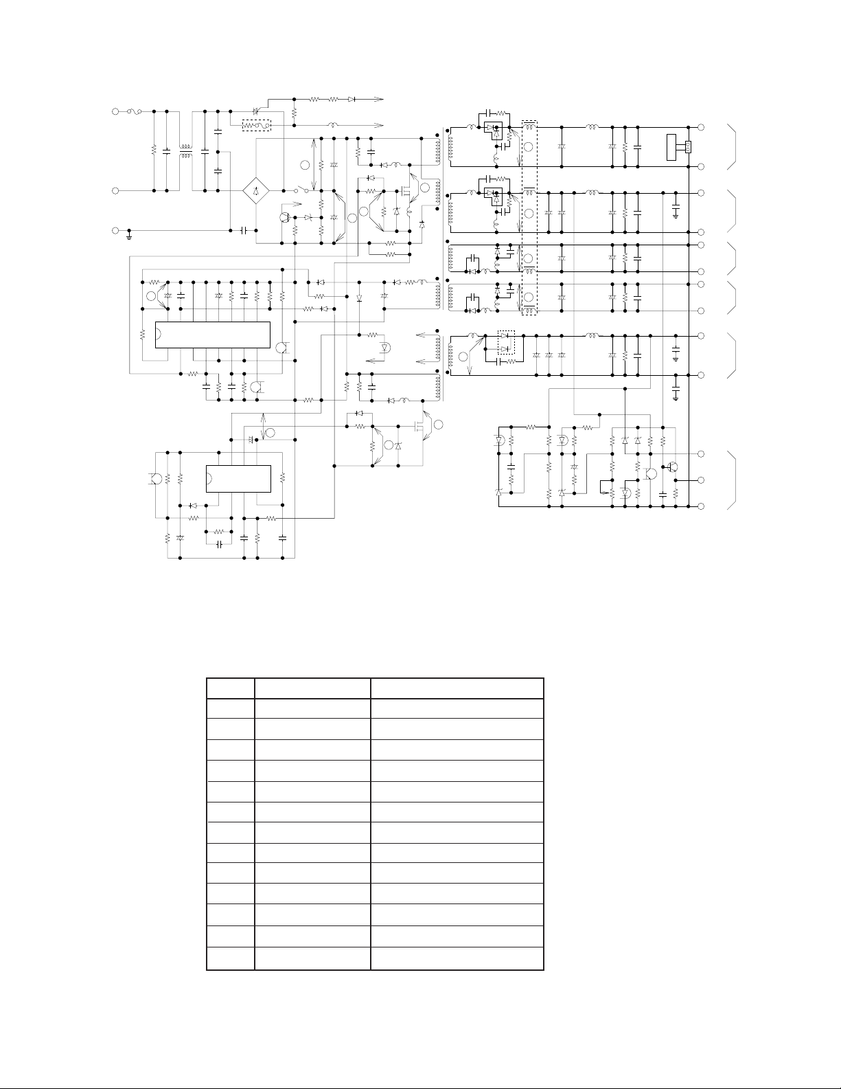
5-9. Power supply circuit
No. Point Voltage level (V)
1 C6 DC180 - 190V
2 C7 DC180 - 190V
3 R21 Less than 30V (Pulse)
4 Q1(D-S) 350 - 400V (Pulse)
5 C24 DC18 - 30V
6 R31 Less than 30V (Pulse)
7 Q2 (D-S) 350 - 400V (Pulse)
8 C31 DC18 - 30V
9 D61 (K-GND) 20V (Pulse)
10 D51 (K-GND) 12V (Pulse)
11 D71 (K-GND) 12V (Pulse)
12 D81 (K-GND) 20V (Pulse)
13 D91 (K-GND) 30V (Pulse)
— 28 —
Page 31

5-10. Printer control PCB(SA-5000)
39
38
37
36
35
34
33
0
P21
P22
P23
P24
P25
P26
P27
P21
P22
P23
P24
P25
P26
P27
P22
P25
P26
P27
R1
R2
R3
R4
P42
P43
P41
P23
P13
P14
P17
P40
IC8
IC8
IC8
P10
IC6
P24
P20
P21
74HC14
74HC14
74HC14
74HC14
74HC14
74HC14
R50
C27
C25
C23
C24
2200pF
1000pF
1000pF
1000pF
1K
R53 R52
R55
R71
C28
C29
C20
4700pF
4700pF
4700pF
1K
R17
3.3K
R18
3.3K
R57
10K
R21
25A1115
4.7K
R63 4.7K
R64
13
IC6F
74LSCF 74LS06
IC6E
12 11 10
1K
R65
C31
0.1
˚
F
1K
R58
10K
C36
0.01
˚
C38
0.01
˚
C39
1000pF
T4T5
2SC2603
2SC2603
E
B
C
E
B
2SC2603
PG
C
E
B
C
T6
E
B
R56
R54
1K
4.7K
R72 1K
R42
1K
R36 1K R35 1K
R49 2.2K
R41 1K
R48 4.7K
R40 4.7K
R34 4.7K
R37
FG
CN3
CN3-1
CN3-2
CN3-3
CN3-4
CN3-5
CN3-6
CN3-7
CN3-8
CN3-9
CN3-10
CN3-11
CN3-12
FG
DRAWER Sol.1
DRAWER SW1
+24 V
NC
GND
FG
DRAWER Sol.2
DRAWER SW2
+24 V
NC
GND
6P*2
DRAWER
4.7K
R38 1K
R39 1K
R59
R60
R61
R62
C
E
T10
25D986
D7
S5566GA
T9
2SD986
4.7K
10K
4.7K
10K
PG
P12
P1[0.7]
PG
74HC14
+24 V
D6
S5566GA
P11 B
B
C
E
2
4
3
0
0
0
6
5
12
13
1
5
1
3
6
2
4
IC7
IC7
IC7
47K
47K
47K
47K
32
26
30
31
CC
IC4
9
C14
R9
4.7K
0.1
˚
F
C13
0.1 ˚F
10
11
74HC14
IC7
74HC14
MS1953B
C15
0.1 ˚F
GND
C18
10pF
X1
C17
10pF
7.3728 MHz
IC8
74HC14
C33
L1
C34
J1
1
3
5
7
9
2
6
4
8
10
+12 V
TXD
RXD
DSR
GND
DTR
RTS
CTS
+5V
NC
TXD
RXD
GND
DTR
1000pf
1000pf
F81
R77
+24 V
+24 V
CN6
1
FB3
GND
R78
0.1
˚
F
R74 T8
CE
B
22K
10K
10K
B
R75
202
PG
A
K
R76
RD8.2EB2
4553
25D1817
25A
115
T11
10K
4.7K
F82
C35
1000pf
C49
15 IC3
R73
47
1 W
C
TC232CPE
R6
47K
C12
C47
25 V 25 V
10
˚
F
10
˚
F
10
˚
F
10 ˚F16 V
C45
C2603
25
T12
+5 V
(0.1
˚
F × 9)
25 V
25 V
VCC
C46
16
C48
10
˚
F
0.14
1
3
C1+
C1–
C2+
C2–
2
6
14
7
13
8
P45
P46
P44
P47
V+
V–
4
5
11
10
12
9
1110
M38002M4-SP
C16
VSS
CNVSS
P2[0:7]
XIN
XOUT
VCC
NC
GND
CD
OUT
1
2
3
4
5
FB4
C43C1C44
C2C3C4
C5
C7C8C9
C10
C11
2,3
100uH
L2
100uH
L3
100uH
T1
T2
R1
R2
GND
TA3
1
2
4
TAB42BK
OC OC
The following circuit is printer control circuit for SA-5000.
A
16 V
GND
X1
7.3728 MHz
C
T3T4T5
E
0.01
C
E
C
E
Color change
R8
A
RA4
2
B1
4
B2
6
B3
8
B4
1
COM1 COM2
PG
B
C36
˚
B
C38
0.01
˚
B
C39
1000pF
PRINTER
CN7
CN7-14
Sol.No1
CN7-6
Sol.No2
CN7-13
4.7K
1K
2SA115
T2
STA4014Y1
3
C1
5
C2
7
C3
9
C4
10
R14
3.3K
R15
3.3K
R19
3.3K
+24 V
FG
C
C41
˚
F
0.1
PG
Sol.No3
CN7-7
Sol.No4
CN7-12
Sol.No5
CN7-4
Sol.No6
CN7-11
Sol.No7
CN7-5
Sol.No8
CN7-3
Sol.No9
CN7-1
+24 V
CN7-8
+24 V
CN7-9
+24 V
CN7-10
+24 V
CN7-15
FG
CN7-2
MOTOR(–)
CN7-16
Sol.PF
CN7-17
Sol.CC
CN7-18
NC
CN4
CN4-1
WIND MOTOR
CN4-2
GMD
R7
100
CN8
CN8-1
+5 V LED
CN8-2
GND LED
CN8-3
(DP)E
CN8-4
(DP)C
CN8-5
(HP)E
CN8-6
(HP)C
CN8-7
RP
CN8-8
NC(VAL)E
NC(VAL)C
NC
Not used
CN8-9
CN8-10
˚
F
Paper feed
74LS06
IC6A
OC
9
8
74LS06
IC6B
OC
5
6
74LS06
IC6C
OC
3
4
74LS06
IC6D
OC
1
2
2SC2603
2SC2603
R17
3.3K
R18
2SC2603
3.3K
R15
3.3K
Head driver
TA1
1
C20
4700pF
4700pF
4700pF
M
C28
C29
C20
0.01˚F
10
11
6
7
9
3
5
7
9
11
13
27
17
19
21
23
25
15
C
RC
A
B
RD
R49 2.2K
VCC
ENA1
IN1
IN2
IN3
IN4
LG1
ENA2
IN5
IN6
IN7
IN8
IN9
LG2
MTA4001M
IC2B
74HC123
R52
R55
R71
2
COM1
4
OUT1
6
OUT2
8
OUT3
10
OUT4
17
GND1
26
COM2
16
OUT5
18
OUT6
20
OUT7
22
OUT8
24
OUT9
14
GND2
5
o
12
o
0
0
0
R48 4.7K
PG PG
22
R13
C21
100 V
1
˚
F
RD24EB3
R54
4.7K
C37
˚
F
CPU
IC1
2
P71
3
P70
4
P67
5
P66
6
P65
7
P64
8
P63
9
P62
10
P61
11
P60
12
P57
13
P56
14
P55
15
P54
16
P53
17
P52
18
P51
19
P50
20
P47
21
P46
22
P45
23
P44
24
P43
25
P42
28
P41
29
P40
27
RESET
1
VCC
32
VSS
26
CNVSS
30
XIN
31
XOUT
M38002M4-SP
IC8
C47
25 V 25 V
˚
F
10
C46
˚
F 25 V
10
P30
P31
P32
P33
P34
P35
P36
P37
P00
P01
P02
P03
P04
P05
P06
P07
P10
P11
P12
P13
P14
P15
P16
P17
P20
P21
P22
P23
P24
P25
P26
P27
1110
74HC14
P30
64
P31
63
P32
62
P33
61
P34
60
P35
59
P36
58
P37
57
56
55
54
53
52
51
50
49
48
P10
47
P11
46
P12
45
P13
44
P14
43
P15
42
P16
41
P17
P20
40
P21
39
P22
38
P23
37
P24
36
35
34
33
C48
10
˚
F
P10
P25
P26
P27
P2[0:7]
47K
P22
R1
47K
P25
R2
47K
P26
R3
47K
P27
R4
12
P42
P43
P41
P23
P13
P14
P17
P40
0.1
P30
P31
P32
P33
P34
P35
P36
P37
+24 V
155355
D1
VR1
500K
2
R10
10K
1
3
R12
10K
C19
220pF
IC8
4
IC8
6
IC6
IC8
2
1
3
74HC14
5
74HC14
13
74HC14
74HC14
R53
R56
R72 1K
R50
1K
1K
1K
C27
Motor
T1
2SD1827
+24 V
EC
C22
0.1
B
ZD1
1
RA3 47K
234
5
— 29 —
Wimding motor control circuit
TXD : Paper end signal
RXD : Data communication between motherboard
DTR : Printer busy signal
Page 32

1
3
5
7
9
100 µK x 4
I
+12 V
I
+IxD
I
+RxD
I
+DSR
I
+GMD
Feed SW.
& LED
L1 L4
2
I
DTR
I
CIS
4
I
RIS
6
I
+5 V
8
I
+MC
10
B4B-XH-A
C13
1000p
L2 L3
5-11. Printer control PCB(SA-5100)
The following circuit is for printer control for SA-5100.
VCC
Q1
2SA1115
R2
CN2
1
2
3
4
C14
1000p
CN4
1
+
3
+
5
+
7
+
9
+
AXL210211
FB4
EXCELSA35
VCC
R4
470
C16
C15
1000p
1000p
VCC
C19
+
0.1 µF
C17
10 µF/25 V
2
+
4
+
6
FB1
+
8
+
10
+
EXCELSA35
+
C26
100 µF/10 V
CPURES
Address latch
4.7K
R3
3.3K
R13
10K
C11
0.1 µF
U1
14
TrD
T1OUT
7
DTR
T2OUT
13
RrD
R1IN
8
DSR
R2IN
16
VCC
2
V+
6
V–
15
GND
C20
TC232CPE
+
10 µF/25 V
VCC
A[0_20]
VCC
R3
VCC
33
D2
1N4148
C10
T1IN
T2IN
R1OUT
R2OUT
VCC
20K 3.3K
AGND
11
10
12
9
1
C1+
3
C1–
4
C2+
5
C2–
U4
19
Q1
18
Q2
17
Q3
16
Q4
15
Q5
14
Q6
13
Q7
12
Q8
74HC573
U5
19
Q1
18
Q2
17
Q3
16
Q4
15
Q5
14
Q6
13
Q7
12
Q8
74HC573
C32
0.1 µF
R16
2K
+
D1
D2
D3
D4
D5
D6
D7
D8
C
OC
D1
D2
D3
D4
D5
D6
D7
D8
C
OC
R16R15
C12
0.01 µF
00R22
+
C21
10 µF/25 V
VCC
2
3
4
5
6
7
8
9
11
1
2
3
4
5
6
7
8
9
11
1
C18
10 µF/25 V
C24
0.1 µF
AD8
AD9
AD10
AD11
AD12
AD13
AD14
AD15
VCC
0.1 µF
AGND
100K R23
AD0
AD1
AD2
AD3
AD4
AD5
AD6
AD7
C34
0.1 µF
A0
A1
A2
A3
A4
A5
A6
A7
VCC
+24 V
A16
A17
A18
A19
A20
A21
A22
A23
A8
A9
A10
A11
A12
A13
A14
A15
C6
VCC
+
656667686970717273747576777879
VSS
VCC
VREF
AVSS
AVCC
P76/AN6
P75/AN5
P83/TXD0
P81/CLK0
P82/RXD0
P80/CTS0/RTS0
P77/AN7/ADTRG
CPU
P24/A20/D4
P25/A21/D5
P26/A22/D6
P27/A23/D7
P30/R/W
P31/BHE
P32/ALE
P33/HLDA
VSSEXOUT
XIN
403938373635343332313029282726
U3A
12
74HC04
21
A1
22
A2
A15
23
A3
24
A4
25
A5
26
A6
A20
27
A7
28
A8
29
A9
31
A10
32
A11
33
A12
34
A13
35
A14
36
A16
37
A17
2
20
C38
100 pF
100K
100KR5R5
P74/AN4
P73/AN3
P72/AN2
P71/AN1
RESET
CNVSS
BYTE
R41
220
R42
1M
14.7456 MHz
R47
33
AGND
80
P67/TB2IN
P66/TB1IN
P65/TB0IN
P64/INT2
P63/INT1
P62/INT0
P61/TA4IN
P60/TA4OUT
P57/TA3IN
P56/TA3OUT
P55/TA2IN
P54/TA2OUT
P53/TA1IN
P52/TA1OUT
P51/TA0IN
P50/TA0OUT
P41/RDY
P40/HOLD
25
R38
10K
VCC
Y1
10 µF/16 V
C3
10 µF/16 V
C31
100 pF
64
63
62
61
60
59
58
57
56
55
54
53
52
51
50
49
48
47
46
45
44
43
42
41
19
18
17
16
15
14
13
12
10
9
8
7
6
5
4
3
38
1
39
P84/CTS1/RTS1
P85/CLK1
P86/RXD1
P87/TXD1
P00/AO
P01/A1
P02/A2
P03/A3
P04/A4
P05/A5
P06/A6
P07/A7
P10/A8/D8
P11/A9/D9
P12/A10/D10
P13/A11/D11
P14/A12/D12
P15/A13/D13
P16/A14/D14
P17/A15/D15
P20/A16/D0
P21/A17/D1
P22/A18/D2
P23/A19/D3
U9
D0
D1
D2
D3
D4
D5
D6
D7
D8
D9
D10
D11
D12
D13
D14
D15
NC
VPP
WE
28 F102FP-10
C6 0.1 µF
R/W#
BHE#
E#
A0
A1
A2
A3
A4
A5
A6
A7
A8
A9
A10
A11
A12
A13
A14
A15
CE
OE
-
+
AD8
AD9
AD10
AD11
AD12
AD13
AD14
AD15
AD0
AD1
AD2
AD3
AD7
AD6
AD5
AD4
AD0
AD1
AD2
AD3
AD4
AD5
AD6
AD7
AD8
AD9
AD10
AD11
AD12
AD13
AD14
AD15
ROM
P70/AN0
P42/@1
Head temperature
C5 0.01 µF
R6
75K
AGND
HEAD_EN#
detection
JUMPER
AGND PGND
DSW1
5
4
VCC
6
3
7
2
8
1
SW DIP-4
1
DIP SW
OFF
ON
OFF
ON
RA1
2
3
4
5
47K x 4
2
3
4
5
R40
47K
U3C
6
74HC14
47K
47K
JP1
2
OFF
OFF
ON
ON
1
RA2
47K x 4
+24 V
100 µF/16 V
5
R48
R50
47K
47K
47K
9600bps
19200bps
28800bps
38400bps
VCC
C33
PGND
PG
R19
R20
R21
1
+
R451KR46
1K
C35
PGND
+24 V
2
4
U6 LB1650
1
INH1
2
IN1
3
OUT1
4
GND
5
GND
6
OUT2
7
IN2
8
VCC1
1000 pF
D12
RL102-E
2SC1815
U3A
74HC14
U3B
74HC14
VCC2
OUT4
OUT3
1
2
4
GND
GND
INH2
U10
Q2
R43
1K
IN4
IN3
R44
4.7K
IN1
IN2
GND
TA8428K
VCC
C1
VP
10 µF/16 VC2100 µF/50 V
+
+
C4
3333R14
R76
2.2K
1/2 W
R76
10K
D4
D5 D6
D8
D9 D10
0.1 µF
R17
33 R25
VCC
Q3
2SD1617
+24 V
RL102-ERL102-E
RL102-ERL102-E
C37
D3
RD10EB2
0.1 µFC30.1 µF
AGND
R30
200
R37
47/1 W
C27
0.1 µF
PGND
D7
RL102-E
D11
RL102-E
VCC
CN1
1
COM
2
COM
3
GND
4
GND
5
LA
6
DI
7
STR9
8
STR8
9
STR7
10
STR6
11
STR5
12
STR4
13
STR3
14
STR2
15
STR1
16
VCC
17
TM
18
TM
19
CP
20
DO
21
PR
22
GND
23
GND
24
COM
25
COM
BS25P-SHF-1AA
CN3
1
2
Paper End
3
4
Head Up
5
6
53047-0610
CN5
1
Near
2
End
5045-02A
CN6
Wind
1
2
Motor
B2B-XH-A
CN7
1
2
Motor
3
4
53047-0410
CN8
1
Auto
2
3
Cutter
4
5267-04A-X
Thermal
Head
VCC
R10
47K
R11
47K
R12
47K
VCC
R26
10K
R27
10K
C22
R26
1000 pF
30K
R29
VCC
+10
OUTA
OUTA
NC
10K
R331KR34
+24 V
R39
10K
VCC
0.1 µF
+24 V
0.1 µF
7
3
5
6
C25
C30
C36
C23
1K
Q4
2SC2603
R31
220
1000 pF
R32
4.7K
0.1 µF
Q13
2SA1115
R77
10K
RL102-E
RL102-E
VCC
1
3
16
15
14
13
12
11
10
9
VCC
R1
56
R3
VCC
22 K
C7
D1
0.1 µF
RD3.9EB2
AGND
U2
M37702
1
2
3
4
5
6
7
8
9
10
11
12
13
14
15
16
17
18
P47
19
P46
20
P45
21
P44
22
P43
23
24
R35
R36
10K
47K
VCC
VCC
C28
22 pF
C29
22 pF
U7A
1
3
2
74AC32
U8B
3
4
74HC04
U7B
5
6
4
74AC32
R49
33
SA-5100 has a thermal printer (LT-380).
To protect the head breakage, CPU control the head temperature and head power supply control.
Temparature Action
Over 60°C Stop printing
Less than 55°C Printing
— 30 —
Page 33

AD[0..15]
A[0..20]
R/W#
BHE#
Data buffer for graphic data : 64KB (32KB x 2)
U7D
A20
12
A15
13
74AC32
A0
RD#
E#
U14B
4
6
5
74AC32
U14D
12
13
11
74AC32
AD8
AD9
AD10
AD11
AD12
AD13
AD14
AD15
VCC VCC
U14A
1
3
2
74AC32
U14C
9
74AC32
8
VCC
10
C46
0.1 µF
11
11
12
13
15
16
17
18
19
WRO#
WRO#
C48
0.1 µF
R61
33
0000H-7FFFH
10000H-17FFFFH
U12
Odd
D1
A0
D2
A1
D3
A2
D4
A3
D5
A4
D6
A5
D7
A6
D8
A7
A8
A9
A10
A11
A12
A13
A14
OE
CS
WE
M5M5256AFP-10L
R62
33
R63
33
0000H-7FFFH
10000H-17FFFFH
Even
A1
10
A2
9
A3
8
A4
7
A5
6
A6
5
A7
4
A8
3
A9
25
A10
24
A11
21
A12
23
A13
2
A14
26
A16
1
22
20
27
AD0
AD1
AD2
AD3
AD4
AD5
AD6
AD7
C47
0.1 µF
11
12
13
15
16
17
18
19
U13
D1
A0
D2
A1
D3
A2
D4
A3
D5
A4
D6
A5
D7
A6
D8
A7
A8
A9
A10
A11
A12
A13
A14
OE
CS
WE
M5M5256AFP-10L
A1
10
A2
9
A3
8
A4
7
A5
6
A6
5
A7
4
A8
3
A9
25
A10
24
A11
21
A12
23
A13
2
A14
26
A16
1
22
20
27
HEAD_EN#
CN10
FB2
1
2
EXCELSA35
3
B3PS-VH
FB3
EXCELSA35
U15
VCC
NC
GND
OUT
M51953AL
Q9
2SA1115
VCC
VCC
R71
4.7K
R74
R79
1K
4.7K
Q12
2SC2603
C51
0.1 µF
R73
1
1K
2
3
4
C
5
C53
0.01 µF
VCC
R69
4.7K
VCC
R72
4.7K
Q11
2SA1115
R75
1K
C52
0.1 µF
R67
4.7K
R70
4.7K
Power control circuit for head
+24V supplies to head when start printing.
6.8K
4.7K
Q10
2SC2603
CPURES#
Q7
R65
R68
2SJ177
SD
R66
22K
Q8
2SC2603
+24 V
+
C50
0.1 µF
C49
100 µF/50 V
VP
R64
10K
— 31 —
Page 34

5-12. Key control PCB
54/CNTR0
51
A5
06/AD6
14
OFF:BCR
ON:K/B
B2B-XH-A
CN19
L9 L8
21
P70
13
12
11
P56/DA1
P57/DA2
P55/CNTR1
P05/AD5
P04/AD4
P03/AD3
52
53
54
A4
A3
A2
P71
P72
10
9
P70/SIN2
P71/SOUT2
P02/AD2
P01/AD1
55
56
A1
A0
P73
P74
8
7
6
P74
P72/SCLK2
P73/SRDY2
P00/AD0
P37/RD
P36/WR
57
58
59
PC K/B,BCR
Select SW
P75
P76
P77
5
4
P75
P76
P77
P35/SYNC
P34/E
P33/RESETOUT
60
61
1
2
3
4
3
2
P60/AN0
P32/ONW
62
63
P30
L1
CORE
S1
Short PAD
1
P61/AN1
P62/AN2
P31
P30
64
P31
P63/AN3
P64/AN5
P65/AN5
P66/AN6
P67/AN7
VCC
8
7
6
5
10 ˚F/16 V
AV55
VREF
VCC
P80
P81
P82
P83
P84
P85
P86
P87
C23
0.01
C32
C33
0.1
80
79
78
77
76
75
74
73
72
71
70
69
68
67
66
65
M38062M3-238FP
R39
R38
R37
R36
R24
P64
P65
P66
10K
P67
˚
VCC
˚
F
P64
P65
P66
P67
VP
U9
D11
D13
D15
D17
MA700 × 4
D23
D25
IN1
IN2
IN3
IN4
IN5
IN6
IN7
IN8
VS
M54564P
U18
IN1
IN2
IN3
IN4
IN5
IN6
IN7
IN8
VS
M54564P
U11
IN1
IN2
IN3
IN4
IN5
IN6
IN7
IN8
VS
M54564P
11
01
12
02
13
03
14
04
15
05
16
06
17
07
18
08
10
GND
11
01
12
02
13
03
14
04
15
05
16
06
17
07
18
08
10
GND
11
01
12
02
13
03
14
04
15
05
16
06
17
07
18
08
10
GND
D10
D12
D14
D16
D22
D24
8
P80
7
P81
6
VCC
47K
47K
47K
47K
VCC
U13E
C31
0.1
23
22
21
20
P80
P81
P82
P83
P84
P85
P86
P87
18
19
U5
A
B
C
D
G1
G2
74HC154
9
1
0
2
1
3
2
4
3
5
4
6
5
7
6
8
7
9
8
10
9
11
10
13
11
14
12
15
13
16
14
17
15
VCC
RA2
10K × 8
P70
P71
P72
P73
P74
P75
P76
P77
CA1
100P × 8
P82
5
P83
4
P84
3
P85
2
P86
1
P87DP
9
P38
P31
P70
P71
P72
P73
P74
P75
P76
P77
8
7
6
5
4
3
2
1
9
8
7
6
5
4
3
2
1
9
21431213651011892143121310118
U12A
74HCB04
MA700 × 16
P70
P71
P72
P73
P74
P75
P76
P77
R35
VCC
47K
VF1
CN6
1
2
3
4
5
B12B-XH-A
6
7
8
9
10
11
12
VFD
1
D38
HA700
2
3
4
5
6
7
8
CN12
9
10
11
B11B-XH-A
VF2
CN1
D2
1
D3
2
D4
3
D5
4
D6
5
D7
6
D8
7
D9
8
9
10
11
12
Key
13
Board
14
15
B24P-SHF-1AA
16
17
18
19
20
21
22
23
24
CON24
8
1
CN3
2
Controll
3
Lock
4
5
B9P-SHF-1AA
6
7
9
CON8
CN4
1
2
Clerk Key
3
4
5
B5P-SHF-1AA
CON5
8G
7G
6G
5G
4G
3G
2G
1G
to SA-5060N
to Keyboard
to Mode key
to Clerk key
SA-5060N : Signal 1 to11
Mode key : Signal 1 to 8
Clerk key : Signal 9 to 12
Keyboard : Signal 1 to 16 : Key common signal
Key input signal
P77
24
P76
23
P75
22
P74
21
20
P73
19
P72
CN2
Signal 17 to 24 : Key input signal
Key common signal
15
1413121110987654321
1516 1413231110987654321
96
104
112
120
128
23
31
39
47
55
127
126
125
124
119
118
117
116
111
110
109
108
103
102
101
100
95
94
93
92
87
86
85
84
83
79
78
77
76
75
71
70
69
68
67
63
62
61
60
59
54
53
52
51
46
45
44
38
37
36
30
29
28
22
21
20
0
15
14
5
4
P71
P70
18
17
121
113
105
97
89
73
81
— 32 —
65
57
49
42
41
34
33
26
25
18
17
10
1
Page 35

5-13. MCR control PCB
0
VCC
C1
Track1
D0
D1
D2
D3
D4
D5
D6
D7
U1
27
D0 TXRDY
28
D1
1
D2
2
D3
5
D4
6
D5
7
D6
8
D7
21
RESET
20
CLK
12
C/D
13
RD
10
WR
11
CS
B251
TXE
TXC
TXD
RXD
RXRDY
RXC
SY/BR
DSR
DTR
CTS
RTS
Track3
D0
D1
D2
D3
D4
D5
D6
D7
D0
D1
D2
D3
D4
D5
D6
D7
U2 ❋
27
D0 TXRDY
28
D1
1
D2
2
D3
5
D4
6
D5
7
D6
8
D7
21
RESET
20
CLK
12
C/D
13
RD
10
WR
11
CS
B251
U3
27
D0 TXRDY
28
D1
1
D2
2
D3
5
D4
6
D5
7
D6
8
D7
21
RESET
20
CLK
12
C/D
13
RD
10
WR
11
CS
B251
TXE
TXC
TXD
RXD
RXRDY
RXC
SY/BR
DSR
DTR
CTS
RTS
Track2
TXE
TXC
TXD
RXD
RXRDY
RXC
SY/BR
DSR
DTR
CTS
RTS
0.1 µF
VCC
4
2
4
2
8
6
C8
.1 µF
U5B
74HC14
U5A
74HC14
U6B
74HC14
U6A
74HC14
U5D
74HC14
U5C
74HC14
312
74HC14
1
VCC
C4
0.1 µF
3
6
74HC14
1
910
74HC14
5
15
18
9
19
3
14
25
16
22
24
17
23
15
18
9
19
3
14
25
16
22
24
17
23
15
18
9
19
3
14
25
16
22
24
17
23
VCC
VCC
R1
100K
C2
0.1 µF
R2
100K
C3
0.1 µF
R3
100K
U5F
U6C
U5E
100K
100K
10
13
VCC
5
VCC
11
U6E
74HC14
VCC
100K
100K
VCC
100K100K
C5
0.1 µ
CN1
12
11
10
9
8
7
6
5
4
3
2
1
CON12
53047-1210
❋ 3 Track Only Use
11
Standard MCR is 2 track system.
To use the 3 track MCR system, replace the MCR unit and mount the IC ( location U2).
5-14. Battery causion
The following ICs have a battery inside.
To carry the motherboard, do not put its solder side on the metal plate.
IC : DS1230Y-200(DALLAS)
IC : DS12887 (DALLAS)
Replace only with the same or equivalent type recommended by the manufacturer.
Dispose of used IC package according to the manufacturer’s instruction.
Remplacez les batteries par un modèle equival lent ou de préférence par celles recommandees
par le constructeur.
Disposez le package IC selon les instructions du constructeur.
Nur mit gleichen, oder vom Herstellen freigegebenen, type ersetzen.
Gebrauchte Gehasuse nur entsprechend den Anwweisungen des Herstellen entsorgen.
— 33 —
Page 36

6. To open / close the upper case
CAUTION : Make sure that the hard disk drive is complete stop before open tha upper case.
Otherwise, the HDD might be defect.
Leave the machine about 40 seconds after power turned off.
1. Release the 4 pcs of screws and lift up the upper case as following figure.
Release these screws.
Also, release oposit side.
Open the upper case like this figure.
— 34 —
Page 37

2. In case the power supply unit is replaced, do not close the air hole of power supply unit.
Air hole
3. To close the upper case, please be careful not to catch the cable between cases or metal plate
when closing the case.
— 35 —
Page 38

7. RESET OPERATION
7-1. Hard reset
It works as PC reset button.
1. Open the upper case.
2. Make short the terminals of JP2 by metal tweezers on the motherboard and turn the power
the power switch on.
3. Wait for 5 seconds and release the tweezers, then hard reset is performed.
7-2. C-MOS reset
It is necessay to clear the data when change the BIOS.
1. Open the upper case.
2. Make short the terminals of JP1 by metal tweezers according to the C-MOS type.
C-MOS Short terminal
DS12887 Pin No.1 and 2
DS12887A Pin No.2 and 3
3. Turn the power switch on with JP1 shorted.
4. Wait for 5 seconds and turn the power switch off.
5. C-MOS reset operation is performed.
6. To conform the reset opeartion, turn the power switch on. Then, the machine is beep and
appears “CMOS ERROR” on the LCD display.
In case this message is not appears, execute 1 to 5 again.
7. Then, Execute “BIOS setup” opearation.
7-3. Memory change
It is necessary to clear the error message when change the memory size.
1. After change the memory size, “ MOMORY SIZE ERROR” appears on the screen.
2. To clear the error message, simply goto “BIOS setup”, and select “SAVE AND EXIT”.
3. Then, memory size is stored in the C-MOS.
— 36 —
Page 39

7-4. BIOS Setup
This chapter provides the user relevant information on setting the BIOS.
The system BIOS used is from AMI. The following is a list of BIOS modifications for the system.
• System setup
• Chipset setup
• Support a maximum of 8 serial ports
• System self test
• Power restore/backup
7-4-1. Defining the Keys
← Left key : key “4” (ASCII 34h) or cursor Left key
→ Right key : key “6” (ASCII 36h) or cursor Right key
↑ Up key : key “8” (ASCII 38h) or cursor Up key
↓ Down key : key “2” (ASCII 32h) or cursor Down key
PageUp
PageDown
Enter Enter key : Enter key (ASCII 0Dh)
Page Up : key “9” (ASCII 39h) or PageUp key
Page Down : key “3” (ASCII 33h) or PageDown key
— 37 —
Page 40

7-4-2. BIOS setup operation
To change the BIOS setup menu
1. Turn the mode key to “5” position.
2. Turn the power switch on.
3. Press “5” button when the AMI BIOS screen appears on the LCD display.
4. Then main menu appears on the LCD display.
7-4-3. Main Menu
The main menu is shown below. The standard display device is usually the VGA CRT on which the
BIOS for a IBM PC-AT compatible will display a full menu. However, in order to use the 2X20 VFD
module for CMOS setting, this format has been modified.
1. Serial Port Setup
2. System Setup
3. Reset to Default Values
4. Save & Quit
5. Exit w/o Saving
When the BIOS system setup is entered, the program will display the first two lines of the main menu
on the operator display (2 x 20 VFD), and the cursor on the display should be set to the first line,
first column.
1 SERIAL PORTS SETUP
2 SYSTEM SETUP
When a Down key is pressed in succession, the cursor on the display will move to the first column on
the next line as well as scroll the display as shown below.
↓
Display:
2 SYSTEM SETUP
3 RESET TO DEFAULTS
↓
Display:
3 RESET TO DEFAULTS
4SAVEANDEXIT
— 38 —
Page 41

↓
Display:
4SAVEANDEXIT
5EXITW/OSAVING
Similarly, when an Up key is pressed, the cursor will move to the upper line as well as scroll the
display.
If the cursor is on the first line, the program will ignore the Up key. Similarly, if the cursor is on the last
line of the menu, the program will ignore the Down key.
To select an item in the main menu, place the cursor on the item and press the <Enter> key.
The program will then display the sub-menu of the selected item.
7-4-3-1. Serial Ports Setup
When the Serial Ports Setup is selected, a sub-menu will be displayed and the cursor will be placed
on the ADDR field.
CUSTOMER D I SPLAY :
ADDR:03F8 INT:4
The Left or Right key should be used to move the cursor between the ADDR and INT field.
The Up and Down key should be used to select one of the available addresses or interrupts.
The available addresses for customer display are 02E8, 02F8, 03E8 and 03F8 and the available
interrupts are 3 and 4.
When a PageDown key is pressed, the operator display option will be displayed with corresponding
address and interrupt setting stored in the RTC’s CMOS. This port and Fiscal port are not used.
OPERATOR DI SPLAY:
ADDR: DIS INT:DIS
When the operator display option is displayed and the PageUp key is pressed, the display will switch
to customer display option.
Likewise, when the PageDown key pressed, the next display will be displayed and so on.
The available addresses for the POS printer, external RS232 #1 - 4 are 02E8, 02F8, 03E8, 03F8,
3220, 3228, 4220 and 4228. The available interrupts are 3, 4, 10, 11, 12 and 15.
At any time when the <Enter> key is pressed, all the setting of the serial port addresses and interrupts
will be saved in a temporary buffer before returning to the Main Menu.
— 39 —
Page 42

POS PR I NTER :
ADDR:03E8 INT:10
F I SCAL PORT :
ADDR: DIS INT:DIS
EXT. RS232 #1:
ADDR:02F8 INT:3
EXT. RS232 #2:
ADDR:02E8 INT:11
EXT. RS232 #3:
ADDR: 4220 INT: 12
EXT. RS232 #4:
ADDR: 4228 INT: 15
7-4-3-2. System Setup
The system setup is as follows:
Date and Time Setting
HDD Setting
Type of Drive
Drive A and B
Boot Sequence and Internal Cache
External Cache and System Shadow Setting
Parity and Video Shadow Setting
Boot ROM Setting
— 40 —
Page 43

When the System Setup is selected, the following figure will be displayed and the cursor is placed on
the date field on first line.
DATE: 23 JAN 1998
TIME(H:M:S) :
hh :mm: ss
The Left key is used to move the cursor from the date field to the month field and from the month field
to the year field. It is also used to move from seconds to minutes and from minutes to hours.
The PageDown key is used to present the next display while the PageUp key is used to present the
previous display.
CYLS:
SECT :
ccc
ss
HEADS :
hh
DRV . A : 1 . 44M 3 . 5 I N
DRV . B : NO
BOOT SEQN . : A , C
I NT . CACHE: D I SABLE
SYST. SHADOW: OFF
EXT . CACHE:D I SABLE
PARI TY : OFF
V I DEO SHADOW: OFF
— 41 —
Page 44

BASE ADDR: 10 0
BOOT ROM: D I S
The <Enter> key is used to exit this setup and return to the Main Menu.
The options available for drive A are:
• 360KB 3.5”
• 720KB 3.5”
• 1.44M 3.5”
• 1.2M 5.25” and
• No.
7-4-3-3. Reset to Default Values
When this sub-menu is selected, the following figure will be displayed.
RESET TO DEFAULTS :
ARE YOU SURE: NO
The Up, Down, Left, Right, PageUp and PageDown keys are used to toggle between the options
Yes and No. The <Enter> key is be used to select the option. If “YES” is selected, all setting available
in this program are reset to default values and return to Main Menu.
7-4-3-4. Save & Exit
When this sub-menu is selected, the program will save all configuration data to CMOS memory and
then re-boot.
7-4-3-5. Exit w/o Saving
Selecting this sub-menu causes the system to reboot without saving any of the setting.
— 42 —
Page 45

8. To change the Monochrome to Color system
Original setting : SA-5000 Monochrome system
SA-5100 Color system
Operator display : SA-5001M Monochrome LCD display
SA-5002C Color LCD display
To mount the color LCD display SA-5002C to SA-5000, the following operation is necessary;
1. Open the upper case.
2. Replace the Video BIOS ROM from Monochrome to Color.
3. Change the jumper of the motherboard as below.
Jumper SA-5001M SA-5002C
JP31 2 - 3 1 - 2
JP46 1 - 2 2 - 3
JP47 1 - 2 1 - 2
CPU
Motherboard
RISER CARD
JP31
JP46 JP47
JUMPER POSITION
— 43 —
Page 46

9. DIAGNOSTIC PROGRAM
1. Diagnoses
(1) BIOS version check (10) Serial port test
(2) Operating system version check (11) Cash drawer test
(3) PC keyboard and memory test (12) Manager key lock test
(4) Clock speed test (13) Ethernet test
(5) Keyboard test (14) MCR test
(6) FDD test (15) Printer test
(7) Customer display test (16) LCD test
(8) NVRAM test (17) DSKBENCH test
(9) LPT test (18) Virus check
2. Necessary tools
(1) PC keyboard (1 unit) (5) CRT (1 unit)
(2) Loop back test connector (6) Customer display (1 unit)
• D-sub 9-pin connector (4 pcs.) (7) MCR card (1 pce)
• D-sub 25-pin connector (1 pce.) (8) Paper roll
• Modular (1 pce.) (9) Ink ribbon
(3) Control key (turns all the way) (10) Diagnostic floppy disk
(4) Cash drawer (2 units)
3. Preparation
(1) Connect loop back test connector to the I/F terminal on the rear panel.
(2) Connect a PC keyboard to Ext.KB which is located on the left side of the SA-5000/5100 and turn
the slide switch to “K” position.
(3) Connect two cash drawer units.
(4) Connect a customer display.
(5) Connect a CRT to Ext.VGA port.
(6) Set a control key on “0” position.
4. System tools
(1) Parallel port loop back plug (5) Magnetic card reader
• Connector: 25-pin D-sub, Male • Magnetic card
• Wiring: connect 1-13, 12-14, 11-17, 10-16, and 2-15 pins (6) Cash drawer interface
• Necessary quantity: 1 pce. • Cash drawer (2 units)
(2) COM port loop back plug
• Connector: 9-pin D-sub, Female
• Wiring: connect 1-7-8, 2-3, and 4-6 pins
• Necessary quantity: 4 pcs.
(3) Network port loop back plug
• Connector: RJ45 8-in
• Wiring: connect 1-3, and 2-6 pins
• Necessary quantity: 1 pce.
(4) Scanner interface
• Keyboard wedge type bar code scanner (1 set)
• Bar code label
— 44 —
Page 47

Operation
To be checked
Print
Turn the power on.
Feed the paper roll using [FEED]
button.
Press [V][E][R] [ENTER] on PC
keyboard.
Press[M][E][M] [ENTER] on PC
keyboard.
Insert diagnostic program FDD in
the slot.
Make sure that BIOS version indication on <screen 1> is 1.3.
• SA-5000/5100 display and the
CRT change to <screen 2>.
• LCD back light turns on.
• Make sure that the LCD contrast
is proper.
• Fan in the power supply unit
turns.
Confirm that the spooler rolls up
the paper while pressing FEED
button.
Display indicates;
MS-DOS Version 6.22
Make sure that the total memory
is 4,096K.
Input [A] [:][ENTER] from SA5000/5100 keyboard.
(To enter [:], press [;] while
pressing down [SHIFT] button.)
[MENU] [ENTER]
[ENTER]
Speed test
[ESC]
Keyboard test
Press [B][Y][E]
Display indicates LANDMARK
screen.
• CPU clock frequency should be
within the range of 560 to 580
MHz.
• FPU clock frequency should be
within the range of 910 to 930
MHz.
When a button is pressed, corresponding button name on the
screen is high lighted.
Press all the buttons to test them.
Display indicates;
Exit Program? (Y/N) : N
CPU & VGA SPEED TESTED
KEYBOARD TESTED
Press [Y]
FDD test
Customer display test
All the segments of the customer
display light.
— 45 —
FDD TEST PASSED
CUSTOMER DISPLAY TESTED
Page 48

Operation
To be checked
Print
NVRAM test
LPT test
Serial port test
Display indicates;
NVRAM Test : Page 0 PASSED
NVRAM Test : Page 1 PASSED
NVRAM Test : Page 2 PASSED
NVRAM Test : Page 3 PASSED
NVRAM Test : Page 4 PASSED
NVRAM Test : Page 5 PASSED
NVRAM Test : Page 6 PASSED
NVRAM Test : Page 0 PASSED
NVRAM Test : Page 1 PASSED
NVRAM Test : Page 2 PASSED
NVRAM Test : Page 3 PASSED
NVRAM Test : Page 4 PASSED
NVRAM Test : Page 5 PASSED
NVRAM Test : Page 6 PASSED
NVRAM Test : Page 7 PASSED
NVRAM Test : Page 7 PASSED
Display indicates;
LPT1 Data Port Test : PASSED
LPT1 Control Port Test : PASSED
LPT1 Data Port Test : PASSED
LPT1 Control Port Test : PASSED
LPT1 Loopback Test : PASSED
LPT1 Loopback Test : PASSED
Display indicates;
Serial Port 1, Base Address = 3F8
Internal Loopback Test PASSED
Serial Port 1, Base Address = 3F8
Internal Loopback Test PASSED
External Loopback Test PASSED
External Loopback Test PASSED
Serial Port 2, Base Address = 2F8
Internal Loopback Test PASSED
External Loopback Test PASSED
Serial Port 2, Base Address = 2F8
Internal Loopback Test PASSED
External Loopback Test PASSED
Serial Port 4, Base Address = 2E8
Internal Loopback Test PASSED
External Loopback Test PASSED
Serial Port 5, Base Address = 3220
Serial Port 4, Base Address = 2E8
Internal Loopback Test PASSED
External Loopback Test PASSED
Internal Loopback Test FAILED
External Loopback Test FAILED
Serial Port 6, Base Address = 3228
Internal Loopback Test FAILED
Serial Port 5, Base Address = 3220
Internal Loopback Test FAILED
External Loopback Test FAILED
External Loopback Test FAILED
Serial Port 7, Base Address = 4220
Internal Loopback Test PASSED
External Loopback Test PASSED
Serial Port 6, Base Address = 3228
Internal Loopback Test FAILED
External Loopback Test FAILED
Serial Port 8, Base Address = 4228
Internal Loopback Test PASSED
External Loopback Test PASSED
Serial Port 7, Base Address = 4220
Internal Loopback Test PASSED
External Loopback Test PASSED
Cash drawer test
Display indicates;
✼✼✼✼✼✼ CASH DRAWER TEST
✼✼✼✼✼✼
Make sure that both drawers open.
— 46 —
Serial Port 8, Base Address = 4228
Internal Loopback Test PASSED
External Loopback Test PASSED
CASH DRAWERS TESTED
Page 49

Operation
To be checked
Print
Manager key lock test
Turn control lock key in the
following order.
0➔1➔2➔OFF➔ON➔5➔6➔7
[ENTER]
Clerk key lock test
[ENTER]
ETHERNET test
MCR test
Read the card while display
indicates;
A : \ >
Display indicates;
✼✼✼✼✼✼ MANAGER KEYLOCK TEST ✼✼✼✼✼✼
TEST KEYLOCK BY TURNING TO DIFFERENT
POSITION (0 TO 7) PRESS [ENTER] KEY TO
END THE TEST
1234567
Display indicates;
✼✼✼✼✼✼ CLERK KEYLOCK TEST ✼✼✼✼✼✼
Test the keylock with different keys Press
[ENTER] key to end the Test
Display indicates;
✼✼✼ NET WORK TEST ✼✼✼
Should be PASSED
Display indicates;
A:\
987654321098765432109876543210987654321098765432
1098765432109876543210987654
Bad command or file name
0
1
2
3
4
5
6
7
MASTER KEY TESTED
OPERATOR KEY TESTED
ETHERNET TEST PASSED
A:\>198506050055555
[T][S][T][9][5][5][ENTER] for SA-5000
[T][S][T][9][5][6][ENTER] for SA-5100
[ENTER]
[ENTER]
[ENTER]
Display indicates;
A : \ > cycle
A : \ > pause
Press any key to continue......
Lines should be square to the display frame.
A : \ > pause
Press any key to continue......
Lines should be square to the display frame.
A : \ > pause
Press any key to continue......
There should be no unevenness
of the color or missing dot.
<SA-5100>
•
•
1014545890101454589010145458901014545890101456458
1014545890101454589010145458901014545890101456458
1014545890101454589010145458901014545890101456458
1014545890101454589010145458901014545890101456458
1014545890101454589010145458901014545890101456458
1014545890101454589010145458901014545890101456458
Auto Half Cut
------------------ – ----------------
— 47 —
Page 50

Operation
To be checked
Print
[ENTER]
[ENTER]
A : \ > pause
Press any key to continue......
A : \ > dskbench C :
DISK Drive Speed TEST v0.03 Copyright
1992 ZOBplus Hayami 500 Kbyte file
Write & Read Testing........
Sequential DISK Write Time : 00.35
Sequential DISK Read Time : 00.28
Random DISK Write Time : 03.57
Random DISK Read Time : 00 .97
A : \ > pause
Press any key to continue .......
A : \ >
A : \ >
<SA-5000>
!”#$%’O*+,-./0123456789:;<=>?@ABCDEFG
HIJKLMNOPQRSTUVWXYZ[\]
pqrstuvwxyz{|}
BBBBBBBBBBBBBBBBBBBBBBBBBBBBB
BBBBBBBBBBBBBBBBBBBBBBBBBBBBB
BBBBBBBBBBBBBBBBBBBBBBBBBBBBB
BBBBBBBBBBBBBBBBBBBBBBBBBBBBB
BBBBBBBBBBBBBBBBBBBBBBBBBBBBB
BBBBBBBBBBBBBBBBBBBBBBBBBBBBB
BBBBBBBBBBBBBBBBBBBBBBBBBBBBB
➠
should be less than 1 second
➠
should be less than 1 second
➠
should be within 3 to 4 seconds
➠
should be less than 1 second
...
abcdefghijklmno
[C][V][ENTER]
[ENTER]
Eject diagnosis floppy disk.
Turn the power off.
Disconnect the cables.
Set the slide switch on “S”.
A : \ > \ cv \ cvakzin C:
•
•
– Hit any key –
•
•
•
325 files have been inspected.
No file has been infected by
known viruses.
A : \ >
Make sure that the unit is not infected.
— 48 —
Page 51

<Screen 1>
American
Megatrends AMIBIOS(C) 1996 American Megatrends Inc.,
Version 1.3
3712KB OK
WAIT...
Auto-Detecting Pri Master..IDE Hard Disk
Auto-Detecting Pri Slave...Not Detected
Pri Master : 02.02.01. ST3850A
(C)American Megatrends Inc.,
41-1000-000000100111111-071595-FINAL-F
<Screen 2>
AMIBIOS System Configuration(C) 1985-1996, American Megatrends Inc.,
Main Processor : Am5x86(X5)-P75 Base Memory Size : 640KB
Main Processor : Built-In Ext. Memory Size : 3072KB
Floppy Drive A: : 1.44 MB 31/2” Display Type : VGA/EGA
Floppy Drive B: : None Serial Port(S) : 3F8,2F8,3E8,2E8
AMIBIOS Date : 07/15/95 Parallel Port(S) : 378
Processor Clock : 133MHz Power Management : Disabled
Hard Disk(S) Cyl Head Sector Size LBA 32Bit Block PIO
Mode Mode Mode Mode
Primary Master : 1648 16 63 811MB LBA Off 16Sec 4
Plug and Play ISA Devices:
AMD PCnet-ISA II Ethernet Network Ad
PCI Devices :
PCI Slot 1 VGA
Extrra COM Ports :: 4220 4228
Starting MS-DOS...
HIMEM is testing extended memory...done.
C: \ > C: \ > DOS \ SMARTDRV.EXE \X
C: \ >
— 49 —
Page 52

10.TROUBLE SHOOTING
Problem Solution
System does not respond a. Check that the system is properly Connected
to the power source
b. Check if the power supply is still working.
If the power supply is not working
( most basic approach is to feel the fan from
the air vent ),
do a thorough check to determine the
cause. Do not attempt to replace the power
supply until the cause is rectified.
No Display but Power supply is working a. Check that the DRAM contact is good.
To confirm, remove the DRAM and Reinsert.
Upon boot up, system stopped after ram a. The K-S switch (keyboard–scanner) Switch
check might be set to “K” but there is no external
keyboard connected.
b. Ram is not compatible with the motherboard.
c. Hard disk (if connected) not detected by BIOS.
Go to BIOS setup and check is HDD is set to
AUTO mode.
If yes but HDD is still not detected, try to check
HDD connection,including the HDD mode
(ie. Master / Slave)
Upon power up, “paper Out” LED blinks a. Paper is jammed on the printer. Open The
printer compartment and rectify The problem.
System experienced intermittent hang a. Check to ensure that the following are
Correct :
1. Jumper setting
2. CPU correctly detected by BIOS
3. Power Supply fan is still working.
4. CPU fan is still working.
“Paper out” LED lights up every time a a. Incorrect baud rate setting.
command is sent to the printer Check that the system is communicating
with the printer at the correct baud rate.
KEYBOARD mapping is lost after a. The system will not hold the new keyboard
Power off mapping.Each time after Power lost,
a “REMAP” need to be executed.
(can be included onto the autoexec.bat file)
Interface card does not work a. Check that the connection is proper
(ie. ISA/PCI card on the riser card) (ie. From interface card to riser card and from
riser card to Motherboard)
b. Check that there are no interrupt conflicts.
Bare in mind that any interface card plugged
onto the riser card takes up interrupt which
has to be released.
Funny display on LCD/CRT a. This will usually happen when the VGA chip
is too hot. Check to ensure There are no
excessive heat built up in the system.
— 50 —
Page 53

11. PCB LAYOUT
11-1. SA-5100 PRINTER CONTROL PCB
— 51 —
Page 54

11-2. SA-5000 PRINTER CONTROL PCB
— 52 —
Page 55

11-3. KEYBOARD CONTROL PCB (SA-5000 / SA-5100)
11-4. MCR CONTROL PCB
— 53 —
Page 56

12. CIRCUIT DIAGRAM
Board Name Drawing No. Model
Motherboard (SA-5000/5100) 1-22 SCH-0160-01 SA-5000/5100
Printer controller without buffer EBL-0329 SA-5000
Printer controller with buffer EBL-0387 SA-5000
Printer controller (1/2) SA-5100
Printer controller (2/2) SA-5100
Keyboard controller (1/3) EBL-0317 SA-5000/5100
Keyboard controller (2/3) EBL-0317 SA-5000/5100
Keyboard controller (3/3) EBL-0317 SA-5000/5100
Keyboard matrix EBK-0146 SA-5000/5100
Key position EBK-0147 SA-5000/5100
Display control (1/2) EAL-0315 SA-5061D
Display control (2/2) EAL-0315 SA-5061D
Display control (1/2) EAL-0327 SA-5062DH
Display control (2/2) EAL-0327 SA-5062DH
Drawer circuit EAC-0065 SA-5000/5100
Power supply circuit KCM150-51C SA-5000/5100
MCR controller EAL-0328 SA-5000/5100
Cable wiring SA-5000
Cable wiring SA-5100
— 54 —
Page 57

ABCDEFGHI JKLMNOP
1
2
3
4
5
1
2
3
4
5
10
6
7
8
9
6
7
8
9
10
Name: Board No. Drawing No.
SCH-0160-01MOTHER BOARD (1/22)SA-5000/5100
ABCDEFGHI JKLMNOP
— 55 —
Page 58

ABCDEFGHI JKLMNOP
1
2
3
4
5
1
2
3
4
5
10
6
7
8
9
6
7
8
9
10
Name: Board No. Drawing No.
SCH-0160-01MOTHER BOARD (2/22)SA-5000/5100
ABCDEFGHI JKLMNOP
— 56 —
Page 59

ABCDEFGHI JKLMNOP
1
2
3
4
5
1
2
3
4
5
10
6
7
8
9
6
7
8
9
10
Name: Board No. Drawing No.
SCH-0160-01MOTHER BOARD (3/22)SA-5000/5100
ABCDEFGHI JKLMNOP
— 57 —
Page 60

ABCDEFGHI JKLMNOP
1
2
3
4
5
1
2
3
4
5
10
6
7
8
9
6
7
8
9
10
Name: Board No. Drawing No.
SCH-0160-01MOTHER BOARD (4/22)SA-5000/5100
ABCDEFGHI JKLMNOP
— 58 —
Page 61

ABCDEFGHI JKLMNOP
1
2
3
4
5
1
2
3
4
5
10
6
7
8
9
6
7
8
9
10
Name: Board No. Drawing No.
SCH-0160-01MOTHER BOARD (5/22)SA-5000/5100
ABCDEFGHI JKLMNOP
— 59 —
Page 62

ABCDEFGHI JKLMNOP
1
2
3
4
5
1
2
3
4
5
10
6
7
8
9
6
7
8
9
10
Name: Board No. Drawing No.
SCH-0160-01MOTHER BOARD (6/22)SA-5000/5100
ABCDEFGHI JKLMNOP
— 60 —
Page 63

ABCDEFGHI JKLMNOP
1
2
3
4
5
1
2
3
4
5
10
6
7
8
9
6
7
8
9
10
Name: Board No. Drawing No.
SCH-0160-01MOTHER BOARD (7/22)SA-5000/5100
ABCDEFGHI JKLMNOP
— 61 —
Page 64

ABCDEFGHI JKLMNOP
1
2
3
4
5
1
2
3
4
5
10
6
7
8
9
6
7
8
9
10
Name: Board No. Drawing No.
SCH-0160-01MOTHER BOARD (8/22)SA-5000/5100
ABCDEFGHI JKLMNOP
— 62 —
Page 65

ABCDEFGHI JKLMNOP
1
2
3
4
5
1
2
3
4
5
10
6
7
8
9
6
7
8
9
10
Name: Board No. Drawing No.
SCH-0160-01MOTHER BOARD (9/22)SA-5000/5100
ABCDEFGHI JKLMNOP
— 63 —
Page 66

ABCDEFGHI JKLMNOP
1
2
3
4
5
1
2
3
4
5
10
6
7
8
9
6
7
8
9
10
Name: Board No. Drawing No.
SCH-0160-01MOTHER BOARD (10/22)SA-5000/5100
ABCDEFGHI JKLMNOP
— 64 —
Page 67

ABCDEFGHI JKLMNOP
1
2
3
4
5
1
2
3
4
5
10
6
7
8
9
6
7
8
9
10
Name: Board No. Drawing No.
SCH-0160-01MOTHER BOARD (11/22)SA-5000/5100
ABCDEFGHI JKLMNOP
— 65 —
Page 68

ABCDEFGHI JKLMNOP
1
2
3
4
5
1
2
3
4
5
10
6
7
8
9
6
7
8
9
10
Name: Board No. Drawing No.
SCH-0160-01MOTHER BOARD (12/22)SA-5000/5100
ABCDEFGHI JKLMNOP
— 66 —
Page 69

ABCDEFGHI JKLMNOP
1
2
3
4
5
1
2
3
4
5
10
6
7
8
9
6
7
8
9
10
Name: Board No. Drawing No.
SCH-0160-01MOTHER BOARD (13/22)SA-5000/5100
ABCDEFGHI JKLMNOP
— 67 —
Page 70

ABCDEFGHI JKLMNOP
1
2
3
4
5
1
2
3
4
5
10
6
7
8
9
6
7
8
9
10
Name: Board No. Drawing No.
SCH-0160-01MOTHER BOARD (14/22)SA-5000/5100
ABCDEFGHI JKLMNOP
— 68 —
Page 71

ABCDEFGHI JKLMNOP
1
2
3
4
5
1
2
3
4
5
10
6
7
8
9
6
7
8
9
10
Name: Board No. Drawing No.
SCH-0160-01MOTHER BOARD (15/22)SA-5000/5100
ABCDEFGHI JKLMNOP
— 69 —
Page 72

ABCDEFGHI JKLMNOP
1
2
3
4
5
1
2
3
4
5
10
6
7
8
9
6
7
8
9
10
Name: Board No. Drawing No.
SCH-0160-01MOTHER BOARD (16/22)SA-5000/5100
ABCDEFGHI JKLMNOP
— 70 —
Page 73

ABCDEFGHI JKLMNOP
1
2
3
4
5
1
2
3
4
5
10
6
7
8
9
6
7
8
9
10
Name: Board No. Drawing No.
SCH-0160-01MOTHER BOARD (17/22)SA-5000/5100
ABCDEFGHI JKLMNOP
— 71 —
Page 74

ABCDEFGHI JKLMNOP
1
2
3
4
5
1
2
3
4
5
10
6
7
8
9
6
7
8
9
10
Name: Board No. Drawing No.
SCH-0160-01MOTHER BOARD (18/22)SA-5000/5100
ABCDEFGHI JKLMNOP
— 72 —
Page 75

ABCDEFGHI JKLMNOP
1
2
3
4
5
1
2
3
4
5
10
6
7
8
9
6
7
8
9
10
Name: Board No. Drawing No.
SCH-0160-01MOTHER BOARD (19/22)SA-5000/5100
ABCDEFGHI JKLMNOP
— 73 —
Page 76

ABCDEFGHI JKLMNOP
1
2
3
4
5
1
2
3
4
5
10
6
7
8
9
6
7
8
9
10
Name: Board No. Drawing No.
SCH-0160-01MOTHER BOARD (20/22)SA-5000/5100
ABCDEFGHI JKLMNOP
— 74 —
Page 77

ABCDEFGHI JKLMNOP
1
2
3
4
5
1
2
3
4
5
10
6
7
8
9
6
7
8
9
10
Name: Board No. Drawing No.
SCH-0160-01MOTHER BOARD (21/22)SA-5000/5100
ABCDEFGHI JKLMNOP
— 75 —
Page 78

ABCDEFGHI JKLMNOP
1
2
3
4
5
1
2
3
4
5
10
6
7
8
9
6
7
8
9
10
Name: Board No. Drawing No.
SCH-0160-01MOTHER BOARD (22/22)SA-5000/5100
ABCDEFGHI JKLMNOP
— 76 —
Page 79

ABCDEFGHI JKLMNOP
10
TA1
1
0.01˚F
M
C20
C28
C29
C20
T10
25D986
6
7
9
10
11
R38 1K
VCC
3
ENA1
5
IN1
7
IN2
9
IN3
11
IN4
13
LG1
27
ENA2
17
IN5
19
IN6
21
IN7
23
IN8
25
IN9
15
LG2
MTA4001M
C
RC
A
B
RD
R49 2.2K
R41 1K
IC2B
74HC123
o
o
R52
0
R55
0
R71
0
COM1
OUT1
OUT2
OUT3
OUT4
GND1
COM2
OUT5
OUT6
OUT7
OUT8
OUT9
GND2
5
12
2
4
6
8
10
17
26
16
18
20
22
24
14
R34 4.7K
R37
FG
PG PG
R48 4.7K
R40 4.7K
4.7K
CN3
6P*2
CN3-1
CN3-2
CN3-3
CN3-4
CN3-5
CN3-6
CN3-7
CN3-8
CN3-9
CN3-10
CN3-11
CN3-12
C21
R13
1
R54
˚
4.7K
F
DRAWER
22
100 V
RD24EB3
FG
DRAWER Sol.1
DRAWER SW1
+24 V
NC
GND
FG
DRAWER Sol.2
DRAWER SW2
+24 V
NC
GND
ZD1
T1
2SD1827
EC
B
RA3 47K
234
R8
RA4
STA4014Y1
B1
B2
B3
B4
COM1 COM2
R14
3.3K
R15
3.3K
R19
3.3K
7
3
5
6
Not mounted.
T6
1K
4.7K
2SA115
C1
C2
C3
C4
+24 V
R20 470
T2
3
5
7
9
10
C30
0.1
+24 V
FG
C
C41
0.1
˚
F
PG
˚
F
74LS06
C31
IC6A
OC
9
8
74LS06
IC6B
OC
5
6
74LS06
IC6C
OC
3
4
74LS06
IC6D
OC
1
2
R15
3.3K
T3T4T5
2SC2603
2SC2603
R17
3.3K
R18
2SC2603
3.3K
R58
10K
PG
R21
4.7K
R64
1K
IC6F
13
˚
F
12 13 1211 10 9 8
OC OC
74LSCF 74LS06 74HC14 74HC14
+24 V
C22
0.1
˚
F
1
5
R57
10K
R65
1K
0.1
A
2
4
6
8
1
PG
C
B
C36
E
0.01
˚
C
B
C38
0.01
˚
E
C
B
C39
E
1000pF
TA3
1
2
4
TAB42BK
B
C
E
25A1115
R63 4.7K
IC6E IC7 IC8
C37
˚
F
1
1
K
RA1
9
8
7
6
5
4
3
2
25
C2603
C2
˚
R76
T12
10
˚
C16
F
C18
10pF
C12
0.14
25A
115
T11
10K
C3
A
16 V
F
GND
X1
7.3728 MHz
10
C49
˚
F
25 V
10
CE
25D1817
R74 T8
22K
4553
10K
R75
+5 V
C4
C5
C46
˚
F
2
6
14
7
13
8
B
K
A
202
PG
10
11
12
13
14
15
16
17
18
19
20
21
22
23
24
25
28
29
27
32
26
30
31
RD8.2EB2
2345678
B
C34
1000pf
C35
1000pf
RA2
100K
P4[0:7]
C33
9
P47
P46
P45
P44
P43
P42
P41
P40
+5 V
C15
0.1
C17
10pF
1000pf
51
52
53
54
55
2
IC2A
74HC123
14
C
15
1
2
3
16
0
RC
A
4
0
B
RD
56
57
58
3
8
C14
0.1
˚
F
4
IC4
VCC
NC
GND
CD
OUT
MS1953B
5
+12 V
6
7
TXD
RXD
DSR
GND
DTR
RTS
CTS
+5V
NC
R9
4.7K
1
2
3
4
5
C13
˚
F
0.1
J1
1
TXD
3
5
RXD
7
GND
9
DTR
2
6
4
8
10
F82
IC7
74HC14
9
IC7
10
74HC14
11
L1
100uH
L2
100uH
L3
100uH
F81
8
R77
10K
9
CN6
+24 V
1
GND
2,3
+24 V
FB3
FB4
C43
˚
F 50 V 100 ˚F16 V
100
PC GND
4.7K
B
R78
C45
16 V
˚
F
10
F
˚
0.1
C1
C44
2
P71
3
P70
4
P67
5
P66
6
P65
7
P64
8
P63
9
P62
P61
P60
P57
P56
P55
P54
P53
P52
P51
P50
P47
P46
P45
P44
P43
P42
P41
P40
RESET
1
VCC
VSS
CNVSS
XIN
XOUT
M38002M4-SP
25 V
16
VCC
V+
V–
R1
R2
15 IC3
(0.1
C7C8C9
C1+
C1–
C2+
C2–
T1
T2
GND
TC232CPE
˚
F × 9)
R73
47
1 W
IC1
IC8
C47
10
1
3
4
5
11
10
12
9
C
P30
P31
P32
P33
P34
P35
P36
P37
P00
P01
P02
P03
P04
P05
P06
P07
P10
P11
P12
P13
P14
P15
P16
P17
P20
P21
P22
P23
P24
P25
P26
P27
1110
74HC14
C48
25 V 25 V
10
˚
F
C10
C11
64
63
62
61
60
59
58
57
56
55
54
53
52
51
50
49
48
47
46
45
44
43
42
41
40
39
38
37
36
35
34
33
˚
R6
47K
P30
P31
P32
P33
P34
P35
P36
P37
P10
P11
P12
P13
P14
P15
P16
P17
P20
P21
P22
P23
P24
P10
P25
P26
P27
P2[0:7]
47K
P22
R1
47K
P25
R2
47K
P26
R3
47K
P27
R4
P42
P43
P41
F
P40
P45
P46
P44
P47
IC8
4
IC8
6
IC6
12
P23
P13
P14
P17
IC8
2
IC7
P24
6
IC7
74HC14
2
P20
IC7
4
P21
+24 V
4.7K
R59
P11 B
R60
10K
P12
4.7K
R61
P1[0.7]
0.1
P30
P31
P32
P33
P34
P35
P36
P37
+24 V
155355
D1
VR1
500K
2
R10
1
3
74HC14
5
74HC14
13
74HC14
74HC14
1
74HC14
5
1
3
74HC14
D6
S5566GA
PG
10K
3
R12
10K
C19
220pF
1K
R53
R56
1K
R72 1K
R50
1K
C27
2200pF
R42
C25
1000pF
1K
R36 1K R35 1K
C23
1000pF
R39 1K
C24
1000pF
C
T9
2SD986
E
D7
S5566GA
PG
B
R62
10K
PG PG FG
4700pF
4700pF
4700pF
C
E
CN7
R7
100
CN5
NEARED.SW
CN4
CN8
CN2
CN7-14
CN7-6
CN7-13
CN7-7
CN7-12
CN7-4
CN7-11
CN7-5
CN7-3
CN7-1
CN7-8
CN7-9
CN7-10
CN7-15
CN7-2
CN7-16
CN7-17
CN7-18
CN4-1
CN4-2
CN8-1
CN8-2
CN8-3
CN8-4
CN8-5
CN8-6
CN8-7
CN8-8
CN8-9
CN8-10
CN5-1
CN5-2
CN5-3
CN5-4
CN1
CN1-1
CN1-2
CN1-3
CN1-4
CN2-1
CN2-2
PRINTER
Sol.No1
Sol.No2
Sol.No3
Sol.No4
Sol.No5
Sol.No6
Sol.No7
Sol.No8
Sol.No9
+24 V
+24 V
+24 V
+24 V
FG
MOTOR(–)
Sol.PF
Sol.CC
NC
WIND MOTOR
GMD
+5 V LED
GND LED
(DP)E
(DP)C
(HP)E
(HP)C
RP
NC(VAL)E
NC(VAL)C
NC
CUT MOT +
CUT MOT –
CUTTER SW
GND
P.ERR LED
PF SW
NC
GND
N.END SW
GND
1
2
3
4
5
Not used
6
Not used
7
8
9
10
Name: Board No. Drawing No.
EBL-0329PRINTER CONTROLLER (1/1)SA-5000
ABCDEFGHI JKLMNOP
— 77 —
Page 80

ABCDEFGHI JKLMNOP
10
VCC
1
2
3
VCC
Q3
2SA1115
R10
C17
1000p
C18
1000p
470
4
Feed SW.
& LED
CN2
B4B-XH-A
C15
1000p
1
2
3
4
C16
1000p
5
TXD
DTR
RXD
+
+
+
+
+
C22
˚
F
2
4
6
8
10
C20
10
˚
F/25 V
FB1
EXCELSA35
DSR
VCC
0.1
˚
H × 4
2:DTR
4:CTS
6:RTS
8:+5V
10:NC
L3L2
L4L1
CN5
1
+
3
+
5
+
7
+
9
+
AXL210211
FB2
EXCELSA35
6
100
7
1:+12 V
3:TXD
5:RXD
7:DSR
9:GND
8
CN8
FB3
1
2
3
B3PS-VH
EXCELSA35
FB4
EEXCELSA35
+24 V
R1
0
VR1
500K 0.5%
R9
4.7K
R13
3.3K
R15
10K
C11
0.1
˚
F
U8
14
T1OUT
7
T2OUT
13
R1IN
8
R2IN
16
VCC
2
V+
6
V–
15
GND
TC232CPE
C23
10
˚
F/25 V
VCC
C31
100
˚
F/10 V
C38
0.1
˚
F
T1IN
T2IN
R1OUT
R2OUT
C1+
C1–
C2+
C2–
C36
100
˚
F/10 V
11
10
12
9
1
3
4
5
+24 v
VCC
180K 0.5%
220pF
P31
P41
C24
10
D1
1SS355TE-17
U2A
14
CEXT
R4
FEED
P45
P47
P44
˚
F/25 V
˚
FILM 1%
0.01
R5
47K
C8
C21
˚
F/25 V
10
VCC
15
REXT/CEXT
1
A
2
B
3
CLR
74HC123
10K
R6
A0
A1
A2
A3
A4
A5
A6
A7
A8
A9
A10
A11
A12
A13
A14
A15
D0
D1
D2
D3
D4
D5
D6
D7
A0
A2
A3
A4
A5
A6
A7
A8
A9
A10
A11
A12
A13
A14
A15
A15
A13
A14
A15
VCC
C37
˚
F
0.1
9
6
7
9
10
11
U2B
CEXT
REXT/CEXT
A
B
CLR
74CH123
5
Q
12
Q
14
13
15
U128
A
B
G
74HC139
12
Y0
11
Y1
10
Y2
9
Y3
1
3
U14A
74LS05
U14B
74LS05
10
25
24
21
23
26
27
22
20
13
9
8
7
6
5
4
3
2
2
3
1
C1
0.1
64
63
62
61
60
59
58
57
56
55
54
53
52
51
50
49
48
47
46
45
44
43
42
41
40
39
38
37
36
35
34
33
U9
A0
A1
A2
A3
A4
A5
A6
A7
A8
A9
A10
A11
A12
A13
A14
OE
CE
27C256
U7F
74HC14
U12A
A
B
G
74CH139
2
4
VCC
˚
F
13
Q
4
Q
P30
P31
P32/ONW
P33/RESETOUT
P34/@
P35/SYNC
P36/WR
P37/RD
P00/AD0
P01/AD1
P02/AD2
P03/AD3
P04/AD4
P05/AD5
P06/AD6
P07/AD7
P10/AD8
P11/AD9
P12/AD10
P13/AD11
P14/AD12
P15/AD13
P16/AD14
P17/AD15
P20/DB0
P21/DB1
P22/DB2
P23/DB3
P24/DB4
P25/DB5
P26/DB6
P27/DB7
M38002
D0
D1
D2
D3
D4
D5
D6
D7
ROM
VPP
12
4
Y0
5
Y1
6
Y2
7
Y3
1
VCC
C2
0.1
˚
F
U3
1
VCC
2
9
9
R2
10K
U10
10
A0
9
A1
8
A2
7
A3
6
A4
5
A5
4
A6
3
A7
25
A8
24
A9
21
A10
23
A11
2
A12
22
OE
20
CS1
26
CS2
27
WE
SRM2264LC10
RA2
47K×8
2
3
4
5
6
7
8
9
1
19
RA3
47K×8
2
3
4
5
6
7
8
9
1
19
˚
F/16 V
VCC
P53/INT5
P52/INT4
P51/INT3
P50/INT2
P45/TXD
P44/RXD
P43/INT1
P42/INT0
CNVSS
RESET
P41/@
XOUT
VSS
C12
VCC
˚
F
P71
P70
P67
P66
P65
P64
P63
P62
P61
P60
P57
P56
P40
XIN
10pF
C13
10pF
12
11
10
9
8
7
16
15
14
13
12
11
10
9
C5
0.1
1
2
3
4
5
6
7
8
9
10
11
12
13
14
15
16
17
18
19
20
21
22
23
24
25
26
27
28
29
30
31
32
7.3728 MHz
VCC
VCC
1
2345678
VCC
2345678
VCC
˚
F
Y1
A0
A1
A2
A3
A4
A5
A6
A7
A8
A9
A10
A11
A12
C33
100pF
C4
10
P55/CNTR1
P54/CNTR0
P47/SRDY
P46/SCLK
11
D0
12
D1
13
D2
15
D3
16
D4
17
D5
18
D6
19
D7
C28
0.1
1
VCC
C34
100pF
DSW1
1
2
3
4
5
6
SW DIP-6
DSW2
SW DIP-8
1
2
3
4
5
6
7
8
U13
A1
A2
A3
A4
A5
A6
A7
A8
G1
G2
74HC541
U15
A1
A2
A3
A4
A5
A6
A7
A8
G1
G2
SW DIP-6
C6
0.01
C35
0.1
D1
D2
D3
D4
D5
D6
D7
D8
3
4
5
R16
R17
Y1
Y2
Y3
Y4
Y5
Y6
Y7
Y8
Y1
Y2
Y3
Y4
Y5
Y6
Y7
Y8
C41
0.1
NC
GND
C
OUT
M51953AL
˚
F
0
0
11
12
13
15
16
17
18
19
C29
0.1
2000h-3FFFh
VCC
PIO A
˚
F
(6000h-6×××)
18
17
16
15
14
13
12
11
PIO B
(4000h-4×××h)
18
17
16
15
14
13
12
11
VCC
˚
F
VCC
D0
D1
D2
D3
D4
D5
D6
D7
VCC
˚
F
D0
D1
D2
D3
D4
D5
D6
D7
D0
D1
D2
D3
D4
D5
D6
D7
PG
JP1
JUMPER
P70
P67
P66
P65
P64
P63
P62
P61
P60
VCC
C7
R8
0
DRW1
P46
DRW2
P51
C39
C40
FG
U1
27
ENA2
25
IN9
23
IN8
21
IN7
19
IN6
17
IN5
15
LG2
13
LG1
11
IN4
9
IN3
7
IN2
5
IN1
3
ENA1
1
VCC
MTA001
˚
F
0.1
MT
P53
U5B
3
P54
CC
74LS06
P55
P54
P50
P42
P43
P40
P52
R35
1K
0.01
R38
1K
0.01
WIND
RP
DP
HP
PE
CUT SW
˚
F
˚
F
9
4
8
U5D
74LS06
U7B
74HC14
U7D
74HC14
C26
0.1
47K
47K
R36
4.7K
PF
VCC
R31
˚
4.7K
5
8
C9
0.1
VCC
F
1
4
74LS06
74LS06
3
9
10
VCC
R37
4.7K
D8
1N4148
COM2
OUT9
OUT8
OUT7
OUT6
OUT5
GND2
GND1
OUT4
OUT3
OUT2
OUT1
COM1
U5A
U5C
VCC
˚
2
6
R29
R30
+24 V
D6
1N4148
F
74HC14
U7C
74HC14
U7E
74HC14
4.7K
D4
R7
26
24
22
20
18
16
14
12
10
8
6
4
2
PGNT
2
6
R27
10K
RL102-E
R32
10K
VCC
U7A
1
5
11
D7
1N4148
D9
1N4148
VCC
1
Q10
2SD986
PGND
R33
4.7K
Q2
2SA115
234
C30
0.01
P57
P5612
+24 V
5
˚
D5
RA1
10K×4
Q6
2SC2603
R20
10K
Q7
2SC2603
Q8
2SC2603
Q9
2SC2603
F
PGND
RL102-E
R34
10K
U6
MT
2
B1
CC
4
B2
PF
6
B3
8
B4
1
COM
R11
10K
R14
10K
45SJ
VCC
R21
3.3K
R23
3.3K
R24
3.3K
R25
3.3K
R26
3.3K
R28
3.3K
U11
IN1
IN2
4
GND
TA8428K
Q11
2SD986
PGND
MP4101
COM
Q5
2SA1115
R18
2.2K
VCC
VCC
+V
OUTA
OUTA
NC
VCC
C1
C2
C3
C4
+24 V
R19
10K
C19
1000pF
C25
1000pF
C27
1000pF
7
3
5
6
3
5
7
9
10
MT
CC
PF
+24 V
D2
RD24EB3
2SD1827
C32
0.1
+24 V
PGND
Q4
D3
RD6.2EB2
C14
0.01
˚
F
R12
471 W
˚
F
PE
PGND
F1
125 V/2 A
Q1
2SD1827
R3
1K
+24 V
CN1
1
2
3
4
5
6
7
8
9
10
11
12
13
14
15
16
17
18
B18P-SHF-1AA
PGND
˚
PGND
CN3
1
2
B28-XH-A
C10
0.1
2
3
4
5
VCC
R22
100
CN4
1
2
3
4
5
6
7
8
9
10
B10P-SHF-1AA
6
7
CN6
1
2
3
4
5267-04A-X
8
CN7
1
2
3
4
5
6
7
8
9
10
11
12
13
FG
TM2REA-1212
PGND
Drawer #1
Drawer #2
9
10
Name: Board No. Drawing No.
EBL-0387PRINTER CONTROLLERSA-5000
ABCDEFGHI JKLMNOP
— 78 —
Page 81

ABCDEFGHI JKLMNOP
10
VCC
P70/AN0
P64/INT2
P63/INT1
P62/INT0
P42/@1
P41/RDY
R38
10K
22 pF
22 pF
1
2
RD#
P47
P46
P45
P44
P43
C29
U7A
74AC32
3
6
R49
33
11
C7
0.1 µF
U2
M37702
1
2
3
4
5
6
7
8
9
10
11
12
13
14
15
16
17
18
19
20
21
22
23
24
VCC
C28
U8B
74HC04
U7B
74AC32
R35
10K
VCC
4
R1
56
D1
RD3.9EB2
AGND
R36
47K
3
5
4
R3
22 K
VCC
C5 0.01 µF
VCC
C45
0.1 µF
R6
75K
AGND
10
12
HEAD_EN#
U3D
8
74HC14
U3E
74HC14
U3F
74HC14
AGND PGND
4
3
2
1
SW DIP-4
9
11
13
DSW1
R54
R59
JP1
JUMPER
PG
R19
47K
R20
47K
R21
R40
47K
R55
VCC
OFF
ON
OFF
ON
1K
0.1 µF
R60
1K
0.1 µF
1
2
3
4
5
2
9600bps
OFF
19200bps
OFF
28800bps
ON
38400bps
ON
1
RA2
47K x 4
+24 V
100 µF/16 V
PGND
5
R48
R50
47K
VCC
1
+
C33
R451KR46
VCC
R57
4.7K
D16
1N4148
R58
4.7K
C35
R51
4.7K
D14
1N4148
1K
PGND
2
4
U6 LB1650
1
INH1
2
IN1
3
OUT1
4
GND
5
GND
6
OUT2
7
IN2
8
VCC1
1000 pF
D12
+24 V
RL102-E
2SC1815
U3A
74HC14
U3B
74HC14
1
2
4
R52
10K
D15
1N4148
D17
1N4148
R43
1K
VCC2
OUT4
GND
GND
OUT3
INH2
R44
4.7K
U10
IN1
IN2
GND
IN4
IN3
VCC
Q2
VCC
1
3
TA8428K
Q5
2SD986
4.7K
16
15
14
13
12
11
10
9
R53
5
6
7
8
DIP SW
RA1
2
3
4
5
47K x 4
U3C
6
74HC14
47K
47K
1K
C40
1K
C43
R26
10K
OUTA
OUTA
+24 V
VCC
+10
NC
VCC
47K
47K
47K
R27
10K
R26
30K
R29
10K
R331KR34
C25
+24 V
R39
10K
VCC
C30
0.1 µF
+24 V
C36
0.1 µF
7
3
5
6
D13
RL102-E
R56
10K
C23
1K
Q4
2SC2603
Q6
2SD986
PGND
R10
R11
R12
C22
1000 pF
R31
220
0.1 µF
R77
10K
1000 pF
R32
4.7K
Q13
2SA1115
RL102-E
RL102-E
3333R14
33 R25
R76
2.2K
1/2 W
R76
10K
+24 V
D4
D5 D6
D8
D9 D10
C37
0.1 µF
+24 V
VCC
Q3
2SD1617
RL102-ERL102-E
RL102-ERL102-E
125 V/2 A
Name: Board No. Drawing No.
SA-5100
PRINTER CONTROLLER (1/2)
CN2
1
2
3
4
C14
C15
1000p
1000p
CN4
2
+
+
4
+
+
6
+
+
8
+
+
10
+
+
AXL210211
FB4
EXCELSA35
65
89
1213
VCC
R4
470
C16
1000p
VCC
C19
0.1 µF
FB1
EXCELSA35
VCC VCC
C41
0.1 µF
Q1
2SA1115
VCC
+
C17
10 µF/25 V
+
R3
3.3K
C11
0.1 µF
TrD
DTR
RrD
DSR
+
VCC
C26
100 µF/10 V
A[0_20]
CPURES
C42
0.1 µF
U7C
9
10
74AC32
R2
4.7K
R13
10K
C20
10 µF/25 V
14
7
13
8
16
2
6
15
8
U1
T1OUT
T2OUT
R1IN
R2IN
VCC
V+
V–
GND
TC232CPE
+24 V
A16
A17
A18
A19
A20
A21
A22
A23
A8
A9
A10
A11
A12
A13
A14
A15
R1OUT
R2OUT
VCC
VCC
T1IN
T2IN
C1+
C1–
C2+
C2–
C32
0.1 µF
VCC
VCC
D2
1N4148
20K 3.3K
R16
2K
AGND
11
10
12
9
1
3
4
5
+
U4
19
Q1
D1
18
Q2
D2
17
Q3
D3
16
Q4
D4
15
Q5
D5
14
Q6
D6
13
Q7
D7
12
Q8
D8
C
OC
74HC573
U5
19
Q1
D1
18
Q2
D2
17
Q3
D3
16
Q4
D4
15
Q5
D5
14
Q6
D6
13
Q7
D7
12
Q8
D8
C
OC
74HC573
AD[0..15]
1
10K x 8
1
10K x 8
R16R15
C12
0.01 µF
00R22
C18
+
10 µF/25 V
C21
10 µF/25 V
VCC
C24
0.1 µF
2
3
4
5
6
7
8
9
11
1
2
3
4
5
6
7
8
9
11
1
VCC
RA3
2
3
4
5
6
7
8
9
RA4
2
3
4
5
6
7
8
9
R3
33
C10
0.1 µF
100K R23
AD0
AD1
AD2
AD3
AD4
AD5
AD6
AD7
AD8
AD9
AD10
AD11
AD12
AD13
AD14
AD15
C34
0.1 µF
AD0
AD1
AD2
AD3
AD4
AD5
AD6
AD7
AD8
AD9
AD10
AD11
AD12
AD13
AD14
AD15
AGND
A0
A1
A2
A3
A4
A5
A6
A7
VCC
AD8
AD9
AD10
AD11
AD12
AD13
AD14
AD15
AD0
AD1
AD2
AD3
AD7
AD6
AD5
AD4
AD0
AD1
AD2
AD3
AD4
AD5
AD6
AD7
AD8
AD9
AD10
AD11
AD12
AD13
AD14
AD15
AD7
AD6
AD5
AD4
AD3
AD2
AD1
AD0
AD15
AD14
AD13
AD12
AD11
AD10
AD9
AD8
VCCVCC
+
C3
10 µF/16 V
C31
100 pF
C6
10 µF/16 V
C6 0.1 µF
64
P84/CTS1/RTS1
63
P85/CLK1
62
P86/RXD1
61
P87/TXD1
60
P00/AO
59
P01/A1
58
P02/A2
57
P03/A3
56
P04/A4
55
P05/A5
54
P06/A6
53
P07/A7
52
P10/A8/D8
51
P11/A9/D9
50
P12/A10/D10
49
P13/A11/D11
48
P14/A12/D12
47
P15/A13/D13
46
P16/A14/D14
45
P17/A15/D15
44
P20/A16/D0
43
P21/A17/D1
42
P22/A18/D2
41
P23/A19/D3
R/W#
BHE#
E#
U9
19
D0
18
17
16
15
14
13
12
10
9
8
7
6
5
4
3
38
1
39
9
11
13
15
19
21
23
25
10
12
14
16
20
22
24
26
6
18
7
27
A0
D1
A1
D2
A2
D3
A3
D4
A4
D5
A5
D6
A6
D7
A7
D8
A8
D9
A9
D10
A10
D11
A11
D12
A12
D13
A13
D14
A14
D15
A15
NC
CE
OE
VPP
WE
28 F102FP-10
8000H-0FFFFH
18000H-1FFFFH
28000H-2FFFFH
38000H-3FFFFH
U11
D0
A0
D1
A1
D2
A2
D3
A3
D4
A4
D5
A5
D6
A6
D7
A7
D8
A8
D9
A9
D10
A10
D11
A11
D12
A12
D13
A13
D14
A14
D15/A-1
A15
NC
A16
A17
A18
VCC
CE
OE
BHE
VSS
NC
VSS
NC
PT500CG2
100000H-1FFFFFH
VCC
+
656667686970717273747576777879
P83/TXD0
P81/CLK0
P82/RXD0
P80/CTS0/RTS0
P24/A20/D4
P25/A21/D5
P26/A22/D6
P27/A23/D7
403938373635343332313029282726
21
22
23
24
25
26
27
28
29
31
32
33
34
35
36
37
2
20
4
3
2
1
44
43
42
41
38
37
36
35
34
33
32
31
30
40
39
5
8
29
28
17
VCC
VREF
AVCC
P30/R/W
P31/BHE
P32/ALE
A1
A2
A3
A4
A5
A6
A7
A8
A9
A10
A11
A12
A13
A14
A16
A17
C38
100 pF
A1
A2
A3
A4
A5
A6
A7
A8
A9
A10
A11
A12
A13
A14
A15
A16
A17
A18
A19
VSS
AVSS
P33/HLDA
VSSEXOUT
VCC
100K
100KR5R5
P76/AN6
P75/AN5
P74/AN4
P73/AN3
P77/AN7/ADTRG
XIN
RESET
CNVSS
R42
1M
14.7456 MHz
U3A
12
74HC04
A15
A20
VCC
A20
C44
100 pF
AGND
80
P72/AN2
P71/AN1
P67/TB2IN
P66/TB1IN
P65/TB0IN
P61/TA4IN
P60/TA4OUT
P57/TA3IN
P56/TA3OUT
P55/TA2IN
P54/TA2OUT
P53/TA1IN
P52/TA1OUT
P51/TA0IN
P50/TA0OUT
BYTE
P40/HOLD
25
VCC
R41
220
Y1
R47
33
C39
0.1 µF
U8E
10
74HC04
1
2
Feed SW.
& LED
B4B-XH-A
C13
1000p
3
L2 L3
4
5
100 µK x 4
1
I+12 V
I+IxD
3
5
I+RxD
I+DSR
7
9
I+GMD
L1 L4
IDTR
2
ICIS
4
6
IRIS
I+5 V
8
10
I+MC
1
3
5
7
9
6
7
8
9
U3C
74HC04
U3D
74HC04
U3F
74HC04
VCC
C1
VP
10 µF/16 VC2100 µF/50 V
+
0.1 µFC30.1 µF
R17
AGND
VCC
R30
200
R37
47/1 W
C27
0.1 µF
PGND
D3
RD10EB2
D7
RL102-E
D11
RL102-E
F1
PG
+
C4
CN1
1
2
3
4
5
6
7
8
9
10
11
12
13
14
15
16
17
18
19
20
21
22
23
24
25
BS25P-SHF-1AA
CN3
1
2
3
4
5
6
53047-0610
CN5
1
2
5045-02A
CN6
1
2
B2B-XH-A
CN7
1
2
3
4
53047-0410
CN8
1
2
3
4
5267-04A-X
CN9
1
2
3
4
5
6
7
8
9
10
11
12
13
TM2REA-1212
COM
COM
GND
GND
LA
DI
STR9
STR8
STR7
STR6
STR5
STR4
STR3
STR2
STR1
VCC
TM
TM
CP
DO
PR
GND
GND
COM
COM
Paper End
Head Up
Near
End
Wind
Motor
Motor
Auto
Cutter
Thermal
Head
Drawer #1
Drawer #2
1
2
3
4
5
6
7
8
9
10
ABCDEFGHI JKLMNOP
— 79 —
Page 82

,
,
,
,
,
,
,
ABCDEFGHI JKLMNOP
10
1
2
9
U7D
12
13
74AC32
R61
11
33
0000H-7FFFH
10000H-17FFFFH
U12
AD8
AD9
AD10
AD11
AD12
AD13
AD14
AD15
VCC VCC
C46
0.1 µF
U14A
WRO#
3
74AC32
U14C
WRO#
8
74AC32
VCC
C48
0.1 µF
Odd
11
D1
12
D2
13
D3
15
D4
16
D5
17
D6
18
D7
19
D8
M5M5256AFP-10L
R62
33
R63
33
A10
A11
A12
A13
A14
OE
WE
CS
A0
A1
A2
A3
A4
A5
A6
A7
A8
A9
A2
9
A3
8
A4
7
A5
6
A6
5
A7
4
A8
3
A9
25
A10
24
A11
21
A12
23
A13
2
A14
26
A16
1
22
20
27
A1
10
AD0
AD1
AD2
AD3
AD4
AD5
AD6
AD7
U13
11
12
13
15
16
17
18
19
C47
0.1 µF
M5M5256AFP-10L
0000H-7FFFH
10000H-17FFFFH
Even
D1
D2
D3
D4
D5
D6
D7
D8
A10
A11
A12
A13
A14
WE
OE
CS
1
2
A0
A1
A2
A3
A4
A5
A6
A7
A8
A9
A2
9
A3
8
A4
7
A5
6
A6
5
A7
4
A8
3
A9
25
A10
24
A11
21
A12
23
A13
2
A14
26
A16
1
22
20
27
3
4
A1
10
5
Memory Map
FFFFFFH
6
120000H
1FFFFFH
,,,,
,,,,
1
AD[0..15]
2
A[0..20]
A0
A20
A15
3
4
RD#
R/W#
BHE#
E#
U14B
12
13
4
5
74AC32
U14D
74AC32
6
10
11
5
6
KANJI
ROM
7
Q7
R65
6.8K
R68
4.7K
Q10
2SC2603
CPURES#
2SJ177
SD
R66
22K
Q8
2SC2603
R64
10K
VP
C50
0.1 µF
+
CN10
1
2
3
B3PS-VH
FB2
EXCELSA35
FB3
EXCELSA35
8
Q9
VCC
9
HEAD_EN#
U15
VCC
NC
GND
C
OUT
M51953AL
C51
VCC
0.1 µF
1
2
3
4
5
C53
0.01 µF
R73
1K
R79
1K
2SA1115
R71
4.7K
Q12
2SC2603
R74
4.7K
VCC
R72
4.7K
VCC
R69
4.7K
Q11
2SA1115
R75
1K
C52
0.1 µF
R67
4.7K
R70
4.7K
+24 V
C49
100 µF/50 V
100000H
,,,,
,,,,
040000H
03FFFFH
038000H
037FFFH
030000H
02FFFFH
028000H
027FFFH
020000H
01FFFFH
018000H
017FFFH
010000H
00FFFFH
008000H
007FFFH
000000H Reserved
,,,,
ROM
,,,,
ROM
,,,,
ROM
RAM
ROM
RAM
7
8
9
10
Name: Board No. Drawing No.
SA-5100
ABCDEFGHI JKLMNOP
— 80 —
PRINTER CONTROLLER (2/2)
Page 83

10
ABCDEFGHI JKLMNOP
VCC VCC VCC
14
2
A12
A13
A14
A15
U14B
74LS07
P45
P43
P44
P45
25
26
27
28
29
30
31
32
33
34
35
36
37
38
39
40
VCC
C30
0.1
˚
1
U15
P42/INT0
CNV55
RESET
P41/E
P40
XIN
XOUT
VSS
P27/DB7
P26/DB6
P25/DB5
P24/DB4
P23/DB3
P22/DB2
P21/DB1
P20/DB0
1
2
3
6
4
5
7
V8
A
B
C
G1
G2A
G2B
74HC138
C29
100P
24
23
22
P44/RXD
P43/INT1
P17/AD15
P16/AD14
41
42
A15
A14
A13
Y0
Y1
Y2
Y3
Y4
Y5
Y6
Y7
C36
0.1
21
20
P45/TXD
P46/SCLK1
P15/AD13
P14/AD12
43
44
45
A12
A11
15
14
13
12
11
10
9
7
˚
INI2
INI3
19
18
17
16
P50
P51/INT2
P52/INT3
P47/SRDY1
P13/AD11
P12/AD10
P11/AD9
P10/AD8
46
47
48
49
A10
A9
A8
A7
VCC
16
8
INI4
R57
D18
151500
18
C24
P47
P46
P45
P44
P43
R58
10K
10K
VCC
P25
18K
˚
/16 V
U14R
10 11
74LS07
C35
˚
0.1
Main
1
KBCLK
KBDATA
CN7
1
2
B4P-SHF-1AA
2
3
B3B-XH-A
CN15
Not mounted
R26
C26
47
47 1/4 W
˚
F/16 V
VCC
4
VCC
J1
VCC
(+5 V)
CN7
4
3
Main
5
6
7
L2
CORE
L3
CORE
VCC
C27
18
P41
P40
U14C
74LS07
U14D
74LS07
C28
22pF
9
˚
F/15 V
65
8
22pF
C25
P40
P41
J2
Y1
10.000 MHz
AT-51
D7
D6
D5
D4
D3
D2
D1
D0
8
9
10
10K
L4
CORE
L5
CORE
˚
10KR46
/16 V
CLOCK
DATA
C34
VCC
L6
100 uH
L7
100 uH
U14E
43
U14F
74LS07
1312
74LS07
CN2
K/B
B6P-SFH-1AA
R47
5
3
1
2
4
5
15
14
13
P53/INT4
P54/CNTR0
P55/CNTR1
P07/AD7
P06/AD6
P05/AD5
50
51
52
A6
A5
A4
P70
12
11
P56/DA1
P57/DA2
P70/SIN2
P04/AD4
P03/AD3
P02/AD2
53
54
A3
A2
OFF:BCR
ON:K/B
P71
P72
10
9
P71/SOUT2
P01/AD1
55
56
A1
A0
CN19
L9 L8
21
PC K/B,BCR
Select SW
1
2
3
4
Short PAD
P73
P74
P75
P76
P77
8
7
6
5
4
3
2
1
P74
P75
P76
P77
P60/AN0
P73/SRDY2
P37/RD
P36/WR
P35/SYNC
57
58
59
RA1
P61/AN1
P34/E
P33/RESETOUT
P32/ONW
P31
60
61
62
63
64
P30
P31
L1
CORE
VCC
P72/SCLK2
P00/AD0
S1
P62/AN2
P30
47K × 8
B2B-XH-A
8
7
6
5
10
P63/AN3
P64/AN5
P65/AN5
P66/AN6
P67/AN7
AV55
VREF
VCC
P80
P81
P82
P83
P84
P85
P86
P87
VCC
5
C32
˚
F/16 V
U13F
74HCB4
47K
47K
47K
47K
47K
47K
47K
47K
C33
0.1
80
79
78
77
76
75
74
73
72
71
70
69
68
67
66
65
6
R39
R38
R37
R36
R24
P64
P65
P66
10K
P67
C23
˚
0.01
VCC
˚
F
P64
P65
P66
P67
M38062M3-238FP
D0
D1
D2
D3
D4
D5
D6
D7
47K
47K
47K
47K
P80
P81
P82
P83
P84
P85
P86
P87
VCC
D0
D1
D2
D3
D4
D5
D6
D7
D0
D1
D2
D3
D4
D5
D6
D7
100P
100P
C
VCC
C
U7
9
D0
10
D1
11
D2
13
D3
14
D4
15
D5
16
D6
17
D7
21
WE
20
OF
18
CE
BR6216B-10LL
U25
11
D0
12
D1
13
D2
15
D3
16
D4
17
D5
18
D6
19
D7
20
CF
22
OE
1
VPP
27C255 (IC Socket)
A10
A10
A11
A12
A13
A14
VP
U9
R35
21431213651011892143121310118
U12A
74HCB04
47K
8
7
6
5
4
3
2
1
9
8
7
6
5
4
3
2
1
9
8
7
6
5
4
3
2
1
9
MA700 × 16
D11
D13
D15
D17
MA700 × 4
D23
D25
IN1
IN2
IN3
IN4
IN5
IN6
IN7
IN8
VS
M54564P
U18
IN1
IN2
IN3
IN4
IN5
IN6
IN7
IN8
VS
M54564P
U11
IN1
IN2
IN3
IN4
IN5
IN6
IN7
IN8
VS
M54564P
RESETOUT#
CLOCKOUT
P80
P81
P82
P83
P84
P85
P86
P87DP
P38
P31
VCC
U5
A
B
C
D
G1
G2
74HC154
A0
A1
A2
A3
A4
A5
A6
A7
A8
A9
A10
C37
0.1
C38
0.1
R15
A0
A1
A2
A3
A4
A5
A6
A7
A8
A9
A10
A11
A12
A13
A14
U13E
9
1
0
2
1
3
2
4
3
5
4
6
5
7
6
8
7
9
8
10
9
11
10
12
11
13
12
14
13
15
14
16
15
VCC
RA2
P70
P71
P72
P73
P74
P75
P76
P77
CA1
100P × 8
R0
VCC
24
˚
12
VCC
28
˚
14
VCC
R44
R43
R42
10K × 8
47K
47K
47K
INT2
INT3
INT4
P70
P71
P72
P73
P74
P75
P76
P77
INT2
INT3
INT4
VCC
P70
P71
P72
P73
P74
P75
P76
P77
C31
0.1
23
22
21
20
18
19
8
A0
7
A1
6
A2
5
A3
4
A4
3
A5
2
A6
1
A7
23
A8
22
A9
19
10
A0
9
A1
8
A2
7
A3
6
A4
5
A5
4
A6
3
A7
25
A8
24
A9
21
23
2
26
27
RD#
WR#
D22
D24
11
01
12
02
13
03
14
04
15
05
16
06
17
07
18
08
10
GND
11
01
12
02
13
03
14
04
15
05
16
06
17
07
18
08
10
GND
11
8G
01
12
7G
02
13
6G
03
14
5G
04
15
4G
05
16
3G
06
17
2G
07
18
1G
08
10
GND
D10
D12
D14
D16
D0
D1
D2
D3
D4
D5
D6
D7
D3
D5
D7
D9
D38
HA700
VCC
VF1
VF2
1
CN6
1
2
3
4
5
B12B-XH-A
6
7
8
9
10
11
12
VFD
1
2
3
4
5
6
7
8
CN12
9
10
11
B11B-XH-A
CN1
D2
1
2
D4
3
4
D6
5
6
D8
7
8
9
10
11
12
Key
13
Board
14
15
B24P-SHF-1AA
16
17
18
19
20
21
22
23
24
CON24
8
1
CN3
2
Controll
3
Lock
4
5
B9P-SHF-1AA
6
7
9
CON8
CN4
1
2
Clerk Key
3
4
5
B5P-SHF-1AA
CON5
1
2
CN5
3
MSR
4
BTK-24P-2S-H
5
6
7
9
10
11
12
13
14
15
16
17
18
19
20
21
22
23
24
CON24
2
3
4
5
6
7
8
9
10
Name: Board No. Drawing No.
SA-5000/5100
KEYBOARD CONTROLLER (1/3)
EBL-0317
ABCDEFGHI JKLMNOP
— 81 —
Page 84

ABCD
1
B4P-SHF-1AA
BACK LIGHT +
4 POWER OFF
5 POWER SW ACTIVE
CN10 B6B-XH-A
R51KUI
R61K
6 UPS OFF
3 BACK LIGHT ON/OFF
1 GND
Vcc (+5 V) CN8
(+5 V) Vcc
11243
C19
0.1 µ
+
C18
10 µ
GND
16 V
GND
C20
+12 V
+
C21
10 µ
0.1 µ
25 V
125 V2A
GND
2
CN14 B2P-SHF-1AA
F2T6
C22
0.1 µ
T7
C2603
2
R23
220 Ω
B744
R22
4.7K
3
4
1
2
3
3
6
5
8
4
R2
Vcc
(+5 V)
Vcc
(+5 V)
D26
5
R3
10K
10K
IN4148
R11K
L10
CN11
9
C9
D27
1
10
14
(+5 V) Vcc
11
0.1 µ
IN4148
L11
2
C10
0.1 µ
7
74HC14
B2B-EH-A
CN13 B2B-XH-A
1
POWER OFF 2
4
5
6
6
Name: Board No. Drawing No.
SA-5000/5100
ABCD
KEYBOARD CONTROLLER (2/3)
— 82 —
EBL-0317
Page 85

ABCD
VP
VF1
VF2
1
R12C4
5 Ω
2
3
3
CVT1
0.1 µ
4
R13
5 Ω
RD9.1EB2(1)
ZD1
5
1
D2
IN4148
D35
D36
9
IN4148
8
D3
R59
RD4.3
EB2
C5
1K
7
2
10K
C7
++
C6
ZD2
470 µ
1000P
T4
R14
1 W
100 Ω
D37
6
220 µ
16 V
IN4148
C3
50 V
+
2SC
1815
500 V
3300P
C8
1 µ 50 V
270 Ω
R15
1
2
3
R11
T3
4
C16
+
C1
5
J4
+5 V
L1 F1 JP1125 V1A
J5
+12 V
390 Ω
R8 R9
51K
(50K)
0.1 µ
470 µ
16 V
T2
2SC1815
C2
680P
R1C
2SC
470 Ω
3303
4
5
6
6
Name: Board No. Drawing No.
SA-5000/5100
ABCD
KEYBOARD CONTROLLER (3/3)
— 83 —
EBL-0317
Page 86

ABCD
1
0
15
2
23
31
39
47
55
3
63
14
22
30
38
46
54
62
5
21
29
37
45
53
61
4
20
28
36
44
52
60
51
59
10
18
26
34
42
1
17
25
33
41
49
57
1
2
3
71
70
69
68
67
79
78
77
76
75
87
86
85
84
83
4
1516 1413231110987654321
1413121110987654321
15
5
CN2
96
104
112
120
128
24
95
103
111
119
127
23
94
102
110
118
126
22
93
101
109
117
125
21
92
100
108
116
124
20
19
18
65
73
81
89
97
105
113
121
17
4
5
P77
P76
P75
P74
P73
P72
P71
P70
6
Name: Board No. Drawing No.
EBK-0146KEYBOARD MATRIXSA-5000/5100
ABCD
— 84 —
6
Page 87

ABCD
1
1
46.3514.00
5.35
25 17
33
28 20 4
36
21 5
29
37
22 14
30
38
2
41
49
57
3
306.70
65
44
52
60
68
45
53
61
69
46
54
62
70
15
31 23
39
47
55
63
71
10
26 18
34
42
51
59
67
1
14.00 46.35
2
3
186.00
73
81
4
97 89
12.35
14.00
5
14.00 80.00 106.00
32.35
113 105
7.0 7.00
121
6
76
84
92
100
108
116
124
77
85
93
101
109
117
125
126.70
133.70
78
86
94
102
110
118126
79
87
95
103
111
119127
75
83
96
112 104
128 120
5.35 5.35
CARBON JAMPEREBK-0146
14.0046.35
4
5
6
Name: Board No. Drawing No.
EBK-0146KEY POSITIONSA-5000/5100
ABCD
— 85 —
Page 88

ABCDEFGHI JKLMNOP
1
VCC
1
202-SD-08GYK
D1
2
151588
3
4
5
6
7
CN1
T × D
3
DTR
8
1
+ 12 V
9
+ 5 V
GND
8
9
2
R × D
5
DSR
7
FB1 F1
FB2
CCV1
(125 V 1 A)
+ 12 V
VCC
C14
0.1 µ
C10
0.1 µ
R1
10K
+
C12
10 µ/10 V
5V1
9
10
11
12
13
14
15
16
5V
VCC
VCC
T × D
–DTR
R × D
–DSR
1 µF
1 µF
DIP-8
C7
C8
VCC
8
7
6
5
4
3
2
1
+ +
RA4
1
1
1
VCC
9876543
1
RA3
47K × 8
RA2
47K × 4
RA1
47K × 4
+
1 µF
47K × 8
C9
2
3
4
5
6
7
8
9
2
3
4
5
2
3
4
5
14
13
16
15
7
8
2
6
2
P57
P56
P55
P54
P53
P52
P51
P50
P47
P46
P45
P44
P43
P42
P41
P40
U3
T1OUT
T2OUT
R1IN
R2IN
V+
VCC
V–
GND
MAX232
P57
P56
P55
P54
P53
P52
P51
P50
P47
P46
P45
P44
P43
P42
P41
P40
C16
0.1 µ
T1IN
T2IN
R1OUT
R2OUT
C1+
C2+
C1–
C2–
7.3728 MHz
11
10
12
9
1
3
4
5
C6
1 µF
VCC
Y1
+
P45
P46
P44
P47
10
11
12
13
14
15
16
17
18
19
20
21
22
23
24
25
26
27
28
29
30
31
32
1
2
3
4
5
6
7
8
9
C3
C4
+
0.1 µF
10 µ/16 V
+
U2
VCC
VREF
AVSS
P67/AN7
P66/AN6
P65/AN5
P64/AN4
P63/AN3
P62/AN2
P61/AN1
P60/AN0
P57/INT3
P56/PWM
P55/CNTR1
P54/CNTR0
P53/SRDY2
P52/SCLK2
P51/SOUT2
P50/SIN2
P47/SRDY1
P46/SCLK1
P45/TXD
P44/RXD
P43/INT2
P42/INT1
CNVSS
RESET
P41/INT0
P40/INT4
XIN
XOUT
VSS
M38022
22 pF
22 pF
C5
1 µF
VCC
C2
R3
P34/C
P36/WR
P37/RD
VCC
64
63
62
61
60
59
58
57
56
55
54
53
52
51
50
49
48
47
46
45
44
43
42
41
40
39
38
37
36
35
34
33
R2
10K
C15
0.1 µF
10K
R4
100K
R5
100K
A0
A1
A2
A3
A4
A5
A6
A7
A8
A9
A10
A11
A12
A13
A14
A15
D0
D1
D2
D3
D4
D5
D6
D7
U4
9
D0
D1
D2
D3
D4
D5
D6
D7
D0
10
D1
11
D2
13
D3
14
D4
15
D5
16
D6
17
D7
21
WE
20
OE
18
CE
BR6216B-10LL
A10
VF1
8
A0
7
A1
6
A2
5
A3
4
A4
3
A5
2
A6
1
A7
23
A8
22
A9
19
C1
P30/DA1
P31/DA2
P32/DNW
P33/RESETOUT
P35/SYNC
P00/AD0
P01/AD1
P02/AD2
P03/AD3
P04/AD4
P05/AD5
P06/AD6
P07/AD7
P10/AD8
P11/AD9
P12/AD10
P13/AD11
P14/AD12
P15/AD13
P16/AD14
P17/AD15
P20/DB0
P21/DB1
P22/DB2
P23/DB3
P24/DB4
P25/DB5
P26/DB6
P27/DB7
123456789
F1F1F1
NP
5-4
4-4
PA54
PA44
1011121314151617181920212223242526272829303132333435363738394041424344454647484950
5-5
4-5
3-5
2-5
1-5
5-6
4-6
3-6
2-6
1-6
5-7
4-7
3-7
2-7
1-7
20G
19G
18G
CURS
PA55
PA45
PA35
PA25
PA15
PA56
PA46
PA36
PA26
PA16
PA57
PA47
PA37
PA27
PA17
PTR2
G20
G19
G18
G17
515253545556575859606162636465666768697071727374757677787980818283
A10
A15
9G8G7G6G5G4G3G2G1G
22G
21G
10G
G9G8G7G6G5G4G3G2G1
G22
G21
G10
C18
220 pF
C17
100 pF
P56
P54
VCC
C11
10 µ/10 V
P57
P51
P52
P50
P53
+
C13
0.1 µF
A0
A1
A2
A3
A4
A5
A6
A7
A8
A9
1-4
2-4
3-4
1-3
2-3
3-3
4-3
5-3
1-2
2-2
3-2
4-2
5-2
PA14
PA24
PA34
PA13
PA23
PA33
PA43
PA53
PA12
PA22
PA32
PA42
PA52
PA11
G1G2G3G4G5G6G7G8G9
VP
81
82
83
84
85
86
87
88
89
90
91
92
93
94
95
96
97
98
99
100
8079787776757473727170696867666564636261605958575655545352
DDG1
DDG2
VDDH
VSS
TEST
SIG
CKG
LHG
BKG
SOG
SIH
SOH
SIA
CKA
LHA
BKA
SOA
SIA
SOB
VDDL
VSS
VDDH
DDG3
DDB20
DDB19
DDB18
123456789
PA11
PA12
PA13
G10
G11
G12
G13
G14
DDG4
DDG5
DDG6
DDG7
DDG8
DDG9
DDG10
DDG11
DDG12
DDG13
DDG14
DDB17
DDB16
DDB15
DDB14
DDB13
DDB12
DDB11
DDB10
DDB9
DDB8
DDB7
101112131415161718192021222324252627282930
PA14
PA15
PA16
PA17
PCOM
PA21
PA22
PA23
PA24
PA25
PA26
17G
G16
1-1
PA21
G15
G16
DDG15
DDB6
PA27
PDP
16G
G15
2-1
PA31
G17
DDG16
DDG17
DDB5
DDB4
PA31
15G
G14
3-1
PA41
G18
G19
DDG18
DDB3
PA32
PA33
14G
G13
4-1
PA51
G20
G21
DDG19
DDG20
DDB2
DDB1
PA34
PA35
13G
G12
5-1
G22
DDH1
DDH2
DDA20
DDA19
PA36
12G
G11
NP
G23
G24
DDH3
DDA18
PA37
PIRI
DDH4
DDA17
11G
40G
39G
G40
G39
84
F2F2F2
G25
G26
G27
G28
DDH5
DDH6
DDH7
DDA16
DDA15
DDA14
PA41
PA42
PA43
PA44
38G
G38
G29
DDH8
DDH9
DDA13
DDA12
PA45
37G
G37
G30
51
DDH10
DDA11
PA46
36G
G36
DDH11
DDH12
DDH13
DDH14
DDH15
DDH16
DDH17
DDH18
DDH19
DDH20
DDA1
DDA2
DDA3
DDA4
DDA5
DDA6
DDA7
DDA8
DDA9
DDA10
35G
G35
VF2
34G
33G
G34
G33
U1
50
49
48
47
46
45
44
43
42
41
40
39
38
37
36
35
34
33
32
31
SED2800FVR
32G
G32
31G
G31
G31
G32
G33
G34
G35
G36
G37
G38
G39
G40
30G
G30
29G
G29
PR57
PR56
PR55
PR54
PR53
PR52
PR51
PTR2
PR47
28G
G28
27G
G27
26G
G26
25G
G25
24G
G24
23G
G23
2
3
4
5
6
7
8
9
10
10
Name: Board No. Drawing No.
EAL-0315DISPLAY CONTROLSA-5061D (1/2)
ABCDEFGHI JKLMNOP
— 86 —
Page 89

ABCD
VP
1
VF1
R12
5 Ω
2
0.1 µ
C24
3
VF2
R13
5 Ω
RD9.1EB2(1)
ZD1
5
4
D2
9
IN4148
D3
IN4148
8
R16
ZD2
RD4.3
EB2
1K
7
10K
C22
220 µ
++
C23
470 µ
16 V
IN4148
1000P
C30
R14
2SC
6
50 V
+
D4
1815
200 Ω
TR3
C24
R15
1
2
1 µ 50 V
3
CVT1
1
2
500 V
1 W
3300P
100 Ω
TR2
2SC
C28
3303
R11
4
R9
390 Ω
R8
50K
+
C21
470 µ
5
J5
16 V
TR1
2SC1815
C27
680P
R1C
470 Ω
3
4
5
+12 V
Vcc
6
6
Name: Board No. Drawing No.
EAL-0315DISPLAY CONTROLSA-5061D (2/2)
ABCD
— 87 —
Page 90

ABCDEFGHI JKLMNOP
1
A10
202-MD-07G
PA11
PA21
PA31
PA41
PA51
PA12
PA22
PA32
PA42
PA52
PA13
PA23
PA33
PA43
PA53
PA14
PA24
PA34
PA44
PA54
PA15
PA25
PA35
PA45
PA55
164163162161160159 158 157156 155154153152151150149148147146145144143142141140139138137136135134133132131130129128127126125124
NPNPNPNPNPICNPNPNPNP1-1A
123122121120119118 117 116115 114113112111110109108107106105104103102101100
NPNP3-6A
4-6A
5-6A
1-7A
2-7A
3-7A
PA36
PA46
PA56
PA17
PA27
PA37
VF1
2-1A
3-1A
4-1A
4-7A
5-7ANPNPNPNPNP20GA
PA47
PA57
PA11
PA21
PA31
PA41
5-1A
PA51
1-2A
G20
PA12
2-2A
19GA
G19
PA22
3-2A
18GA
G18
PA32
4-2A
17GA
G17
PA42
5-2A
16GA
G16
PA52
1-3A
15GA
G15
PA13
2-3A
3-3A
4-3A
5-3A
1-4A
2-4A
3-4A
4-4A
5-4A
1-5A
2-5A
3-5A
4-5A
99 98 97 9695 94 93 92 91 90 89 88 87 86 85 84 83
14GA
13GA
12GA
11GA
10GA
9GA
8GA
7GA
6GA
5GA
4GA
3GA
2GA
G14
G13
G12
G11
G10G9G8G7G6G5G4G3G2
PA23
PA33
PA43
PA53
PA14
PA24
PA34
PA44
PA54
PA15
PA25
PA35
PA45
G1
PA55
1 2 3 4 5 6 7 8 9 1011121314151617181920212223242526272829303132333435363738394041
F1F1F1NPNPICNPNPNPNP1-1B
2-1B
3-1B
4-1B
5-1B
1-2B
2-2B
3-2B
4-2B
5-2B
1-3B
2-3B
3-3B
4-3B
5-3B
1-4B
2-4B
3-4B
4-4B
5-4B
1-5B
2-5B
3-5B
4-5B
PA16
PA26
5-5A
1-6A
2-6ANPNPFdFd
1GANPNPNPNPNPNP
PA16
PA26
5-5B
1-6B
2-6BNPNPFdFd
R6
33K
R7
33K
VP
VP
42 43 44 45 46 47 48 49 50 51 52 53 54 55 56 57 58 5960 61 62 63 64 65 66 67 68 69 70 71 72 73 74 75 7677 78 79 80 81 82
NPNP3-6B
4-6B
5-6B
1-7B
2-7B
3-7B
4-7B
5-7B
DesNPNPNPNP
PA36
PA46
PA56
PA17
PA27
PA37
PA47
PA57
PTR2
C18
220 pF
C17
100 pF
P56
P54
VCC
C11
10 µ/10 V
P57
P51
P52
P50
P53
8
A0
A1
A2
A3
A4
A5
A6
A7
A8
A9
A0
7
A1
6
A2
5
A3
4
A4
3
A5
2
A6
1
A7
23
A8
22
A9
19
A10
A15
VP
81
82
83
84
85
86
87
88
89
90
91
92
93
94
95
96
97
98
99
C13
0.1 µF
100
+
20GB
19GB
18GB
17GB
16GB
15GB
14GB
13GB
12GB
11GB
10GB
G40
G39
G38
G37
G36
G35
G34
G33
G32
G31
G30
G1G2G3G4G5G6G7G8G9
8079787776757473727170696867666564636261605958575655545352
DDG1
DDG2
VDDH
VSS
TEST
SIG
CKG
LHG
BKG
SOG
SIH
SOH
SIA
CKA
LHA
BKA
SOA
SIA
SOB
VDDL
VSS
VDDH
DDG3
DDB20
DDB19
DDB18
123456789
PA11
PA12
PA13
G10
G11
G12
G13
G14
G15
G16
G17
DDG4
DDG5
DDG6
DDG7
DDG8
DDG9
DDG10
DDG11
DDG12
DDG13
DDG14
DDG15
DDG16
DDB17
DDB16
DDB15
DDB14
DDB13
DDB12
DDB11
DDB10
DDB9
DDB8
DDB7
DDB6
PA23
PA24
PA25
PA26
PA27
PDP
DDB5
PA31
101112131415161718192021222324252627282930
PA14
PA15
PA16
PA17
PCOM
PA21
PA22
DDG17
DDB4
G29
G18
G19
DDG18
DDB3
PA32
PA33
9GB
G28
G20
DDG19
DDG20
DDB2
DDB1
PA34
8GB
G21
DDH1
DDA20
PA35
7GB
G27
G22
G23
DDH2
DDA19
PA36
PA37
6GB
G26
G24
DDH3
DDH4
DDA18
DDA17
PIRI
G25
G25
G26
DDH5
DDA16
PA41
PA42
5GB
G24
G27
DDH6
DDH7
DDA15
DDA14
PA43
4GB
G28
DDH8
DDA13
PA44
3GB
G23
G29
DDH9
DDA12
PA45
G22
G30
51
DDH10
DDA11
PA46
2GB
G21
DDH11
DDH12
DDH13
DDH14
DDH15
DDH16
DDH17
DDH18
DDH19
DDH20
DDA10
1GBNPNPNPF2F2F2
U1
50
G31
49
G32
48
G33
47
G34
46
G35
45
G36
44
G37
43
G38
42
G39
41
G40
40
DDA1
39
DDA2
38
DDA3
37
DDA4
36
DDA5
35
DDA6
34
DDA7
33
DDA8
DDA9
32
31
SED2800FVR
PTR2
PR57
PR56
PR55
PR54
PR53
PR52
PR51
PR47
VF2
151588
C10
0.1 µ
VCC
D1
R1
10K
+
C12
10 µ/10 V
5V1
9
10
11
12
13
14
15
16
5V
VCC
VCC
T × D
–DTR
R × D
–DSR
1 µF
1 µF
DIP-8
C7
C8
VCC
8
7
6
5
4
3
2
1
+ +
RA4
1
1
1
VCC
2345678
1
RA3
47K × 8
RA2
47K × 4
RA1
47K × 4
+
1 µF
47K × 8
C9
2
3
4
5
6
7
8
9
2
3
4
5
2
3
4
5
14
13
16
15
7
8
2
6
9
P57
P56
P55
P54
P53
P52
P51
P50
P47
P46
P45
P44
P43
P42
P41
P40
U3
T1OUT
T2OUT
R1IN
R2IN
V+
VCC
V–
GND
MAX232
P57
P56
P55
P54
P53
P52
P51
P50
P47
P46
P45
P44
P43
P42
P41
P40
C16
0.1 µ
J1
J2
J3
J4
T1IN
T2IN
R1OUT
R2OUT
C1+
C1–
C2+
C2–
7.3728 MHz
11
10
12
9
1
3
4
5
C6
1 µF
VCC
Y1
P45
P46
P44
P47
P45
P46
P44
P47
+
0.1 µF
1
2
3
4
5
6
7
8
9
10
11
12
13
14
15
16
17
18
19
20
21
22
23
24
25
26
27
28
29
30
31
32
C3
C4
+
10 µ/16 V
+
U2
VCC
VREF
AVSS
P67/AN7
P66/AN6
P65/AN5
P64/AN4
P63/AN3
P62/AN2
P61/AN1
P60/AN0
P57/INT3
P56/PWM
P55/CNTR1
P54/CNTR0
P53/SRDY2
P52/SCLK2
P51/SOUT2
P50/SIN2
P47/SRDY1
P46/SCLK1
P45/TXD
P44/RXD
P43/INT2
P42/INT1
CNVSS
RESET
P41/INT0
P40/INT4
XIN
XOUT
VSS
M38022
22 pF
22 pF
C5
1 µF
VCC
C2
R3
P34/C
P36/WR
P37/RD
VCC
64
63
62
61
60
59
58
57
56
55
54
53
52
51
50
49
48
47
46
45
44
43
42
41
40
39
38
37
36
35
34
33
R2
10K
C15
0.1 µF
10K
R4
100K
R5
100K
A0
A1
A2
A3
A4
A5
A6
A7
A8
A9
A10
A11
A12
A13
A14
A15
D0
D1
D2
D3
D4
D5
D6
D7
U4
9
D0
D1
D2
D3
D4
D5
D6
D7
D0
10
D1
11
D2
13
D3
14
D4
15
D5
16
D6
17
D7
21
WE
20
OE
18
CE
BR6216B-10LL
C1
P30/DA1
P31/DA2
P32/DNW
P33/RESETOUT
P35/SYNC
P00/AD0
P01/AD1
P02/AD2
P03/AD3
P04/AD4
P05/AD5
P06/AD6
P07/AD7
P10/AD8
P11/AD9
P12/AD10
P13/AD11
P14/AD12
P15/AD13
P16/AD14
P17/AD15
P20/DB0
P21/DB1
P22/DB2
P23/DB3
P24/DB4
P25/DB5
P26/DB6
P27/DB7
2
3
4
5
6
7
8
9
+ 12 V
+ 5 V
GND
1
8
9
CN1
6
RTS
3
T × D
2
DTR
5
R × D
7
DSR
FB1 F1
FB2
CCV1
(125 V 1 A)
VCC
+ 12 VF2
C14
0.1 µ
1
2
3
4
5
6
7
8
9
10
10
Name: Board No. Drawing No.
EAL-0327DISPLAY CONTROL (1/2)SA-5062DH
ABCDEFGHI JKLMNOP
— 88 —
Page 91

ABCD
VP
1
VF1
R12
2
0.1 µ
C24
3
VF2
R13
RD9.1EB2(1)
ZD1
5
4
D2
9
IN4148
D3
IN4148
8
R16
ZD2
RD4.3
EB2
1K
7
10K
C22
220 µ
++
C23
470 µ
16 V
IN4148
1000P
C30
R14
2SC
6
50 V
+
D4
1815
200 Ω
TR3
C24
R15
1
2
1 µ 50 V
3
CVT1
1
2
500 V
1 W
3300P
100 Ω
TR2
2SC
3303
C28
R11
4
R9
390 Ω
R8
50K
+
C21
470 µ
5
J5
16 V
TR1
2SC1815
C27
680P
R1C
470 Ω
3
4
5
+12 V
Vcc
6
6
Name: Board No. Drawing No.
EAL-0327DISPLAY CONTROL (2/2)SA-5062DH (1/2)
ABCD
— 89 —
Page 92

ABCD
1
2
1
2
CN
FG
1
DC24V
3
DRAWER KICK
DRIVE
OPEN/CLOSE
2
3
3
SIGNAL
+24 V
4
NC
5
SG
6
4
5
6
4
5
6
Name: Board No. Drawing No.
EAC-0065DRAWER CIRCUITSA-5000/5100
ABCD
— 90 —
Page 93

ABCDEFGHI JKLMNOP
D6
R12A
R12B
P4
C20
R21
+
R7
D4
C8
C30
A
B
D9
L4
Z1
D3
Q1
L5
R10 L3
L6
A'
B'
Q2
R61C61
T1
L61
C51
D61
L62
C62
R51
R62
9
+ +
C63
L63
C64
R63
C65
FAN1
4
D5
T2
L91
L51
C71
D71
C81
D81
D51
C52
L52
D72
L71
D82
L81
D91
L53 L54
+
10
R52
11
C72
L72
12
C82
L82
+
+ +
+ +
C53
C54
+
C73
+
C83
L92
C74
C84
+
C56
R53
C55
+
C75C85
R71
+
R81
13
R91C91
C92
C93
C94
C95
R92
C96
C42C44C43
CN1
+12 V
DC+12V
GND
+5 V
DC+5V
GND
GND
DC-5V
–5 V
GND
DC-12V
–12 V
+24 V
DC+24V
GND
1
2
3
4
5
6
7
1
AC L
F1
TR1
R13
R2
2
C1
L1
C2
C4 C3
C5
D1
1
SW1
C
Z3
Q3
R6
R1
AC N
3
FG
R14A
R14B D2
L2
+
R3
R4
+
R5
C7
R20
C6
R22
3
2
4
R11
R24
R17
D8
R8
D7
R9
D11
C'
R30
D10
5
5
R23
6
7
C24
C23
+ +
16 15 14 13 12
1234
R28
C22
IC1
C25
11 10 9
5
678
C26
R16
R27
R29
C21
P1
R26
R25
R15
P3
7
8
8765
R34
9
P2
R33
123
D12
+
C31
IC2
8
4
R32
R31
R95
6
Z2
IC91
R96R97 C97
P1P2
R98 R94 R93
IC51
R56
R42
R60
P4
R41
C41
Q41
R43
P.F
P.G
GND
DC+24V
R57
+
C57
R58
R54R55
R59
P3
VR51
Z51
Z91
8
9
10
R36
R35
+
C32
R37
C34
C33
R39
R40
10
C35 R38
Name: Board No. Drawing No.
KCM150-51CPOWER SUPPLY UNIT
ABCDEFGHI JKLMNOP
— 91 —
Page 94

ABCDEFGHI JKLMNOP
1
2
3
4
5
6
VCC
10 µF/16 V
CN2
1
0.1 µF
2
3
4
5
6
7
8
9
10
11
12
13
14
15
16
17
18
19
20
21
22
23
24
CON24
BTK24S-2S
C6
C7
D0
D1
D2
D3
D4
D5
D6
D7
13
U6F
74HC14
D0
D1
D2
D3
D4
D5
D6
D7
D0
D1
D2
D3
D4
D5
D6
D7
12
U1
27
D0 TXRDY
28
D1
1
D2
2
D3
5
D4
6
D5
7
D6
8
D7
21
RESET
20
CLK
12
C/D
13
RD
10
WR
11
CS
B251
U2 ❋
27
D0 TXRDY
28
D1
1
D2
2
D3
5
D4
6
D5
7
D6
8
D7
21
RESET
20
CLK
12
C/D
13
RD
10
WR
11
CS
B251
TXE
TXC
TXD
RXD
RXRDY
RXC
SY/BR
DSR
DTR
CTS
RTS
TXE
TXC
TXD
RXD
RXRDY
RXC
SY/BR
DSR
DTR
CTS
RTS
VCC
C1
0.1 µF
U5F
74HC14
C4
0.1 µF
U6C
6
74HC14
15
18
9
19
3
14
25
16
22
24
17
23
15
18
9
19
3
14
25
16
22
24
17
23
R1
100K
VCC
C2
0.1 µF
R2
100K
4
2
4
2
U5B
312
74HC14
U5A
1
74HC14
VCC
U6B
3
74HC14
U6A
1
74HC14
100K
13
VCC
5
VCC
VCC
100K
VCC
100K100K
C5
0.1 µ
CN1
12
11
10
9
8
7
6
5
4
3
2
1
CON12
53047-1210
1
2
3
4
5
6
10
7
D0
D1
D2
D3
D4
D5
D6
8
D7
U3
27
D0 TXRDY
28
D1
1
D2
2
D3
5
D4
6
D5
7
D6
8
D7
21
RESET
20
CLK
12
C/D
13
RD
10
WR
11
CS
B251
TXE
TXC
TXD
RXD
RXRDY
RXC
SY/BR
DSR
DTR
CTS
RTS
15
18
19
14
25
16
22
24
17
23
9
VCC
C3
9
3
0.1 µF
R3
100K
VCC
8
6
C8
0.1 µF
U5D
910
74HC14
U5C
5
74HC14
U5E
74HC14
10
8
100K
11
U6E
74HC14
U6D
74HC14
11
9
100K
❋ 3 Track Only Use
7
8
9
10
Name: Board No. Drawing No.
EAL-0328MCR CONTROLLERSA-5000/5100
ABCDEFGHI JKLMNOP
— 92 —
Page 95

SA-5000 CABLE WIRING
K/B BCR Sw
EXT. K/B
K/B Cont
CN2
K/B Cont
CN19
K/B Cont
CN11
INLET
POWER
SWITCH
M/B
2 × 20 VFD
K/B Cont
P/S
232C#1
J13
PS3
CN10
VR
J9
K/B Cont
CN7
J7
J4
232C#1
J8
RISER CARD
J3 EMI BOARD
J4
J3
Black
PS1
H/B J1
FDD
2 × 20 VFD
J2
Black
CPU
J1
LCD
+24 V
HDD
Printer Cont.
CFL
K/B Cont
CN14
K/B Cont
CN14
HDD
MCR Cont CN1
MCR
K/B Cont
CN8
CN7
CN6
CN12
CN14
CN8 CN10
J1
Printer Cont.
WIND MOTOR
CN8
PRINTER
K/B
CN6 CN2 CN1
CN1
CN7
FEED SW
MCR Cont.
CN1
MODE
SW
CN3
CN4 CN19 CN11
Black color cable cames center.
Bottom Case Upper Case
VR
— 93 —
CLERK
CN13
K/B Cont.
Page 96

SA-5100 CABLE WIRING
K/B BCR Sw
EXT. K/B
K/B Cont
CN2
K/B Cont
CN19
K/B Cont
CN11
INLET
POWER
SWITCH
M/B
2 × 20 VFD
K/B Cont
P/S
232C#1
J13
PS3
CN10
VR
J9
K/B Cont
CN7
J7
J4
232C#1
J8
RISER CARD
J3 EMI BOARD
J4
J3
Black
PS1
H/B J1
FDD
2 × 20 VFD
J2
Black
CPU
J1
LCD
+24 V
HDD
Printer Cont.
CFL
K/B Cont
CN14
K/B Cont
CN14
HDD
MCR Cont CN1
MCR
K/B Cont
CN8
WIND
MOTOR
CN7
CN14
CN8 CN10
CN6
CN12
CN4
Printer Cont.
CN6
CN7
PRINTER
K/B
CN6 CN2 CN1
CN1
FEED SW
CN1
MCR Cont.
CN3
MODE
SW
CN2
CN8
AUTO
CUTTER
CN3
CN4 CN9 CN11
Black color cable cames center.
Bottom Case Upper Case
VR
— 94 —
CLERK
CN13
K/B Cont.
Page 97

13. PARTS LIST
1. SA-5000 ..................................................................................................... 96
2. SA-5100 ...................................................................................................105
3. SA-5001M / 5002C...................................................................................113
4. SA-5060N / SA-5061D / SA-5062DH....................................................... 117
5. DL-2909 ...................................................................................................123
6. DL-2765 ...................................................................................................125
Notes:
1. Prices and specifications are subject to change without notice.
2. As for order / supply of spare parts, refer to the "GUIDEBOOK for Spare Parts Supply", a separate
publication.
3. The numbers in item column correspond to the same numbers in drawing.
4. MARKS:
Q: Quantity used per unit
R: Rank
A: Essential
B: Stock recommended
C: Less recommended
X: No stock recommended
— 95 —
Page 98

SA-5000
— 96 —
Page 99

SA-5000
PRINTER CONTROLLER
Item Code No. Parts Name Specification Q R
PCB EBL-0387
U4 1904 8623 LSI M38002M4-XXSP 00508345(OTP) 1 A
U8 1904 8481 IC TC232CPE 00501420 1 A
U7 1904 8624 IC/MOS TC74HC14AP 00606290 1 A
U2 1904 8625 IC/MOS TC74HC123AP 00606531 1 A
U3 1904 8492 IC M51953AL 00600265 1 A
U5 1904 8626 IC/TTL HD74LS06P 00608012 1 A
U10 1904 8627 LSI/S-RAM BR6265-10LL (SRM2264LC-10) 00502210 1 A
U1 1904 8628 IC MTA001M-F4101 00600810 1 A
U12 1904 8629 IC/MOS TC74HC139AP 00606150 1 A
U13.15 1904 8630 IC/MOS TC74HC541AP 00608150 2 A
Q6-9 1904 8494 TRANSISTOR 2SC2603 00700630 4 B
Q4 1904 8495 TRANSISTOR 2SD1817 00700190 1 B
Q1 1904 8631 TRANSISTOR 2SD1827 00700150 1 B
Q10.11 1904 8496 TRANSISTOR 2SD986 00700240 2 B
Q2.3.5 1904 8493 TRANSISTOR 2SA1115 00700570 3 B
U6 1904 8632 TRANSISTOR/ARRAY STA401A 00703010 1 A
D1 1904 8633 DIODE 1SS136 00800500 1 B
D4.5 1904 8501 DIODE RL102-E 00800915 2 B
D2 1904 8634 DIODE/ZENER RD24EB3 01000363 1 B
D3 1904 8500 DIODE/ZENER RD8.2EB2 01000170 1 B
CAPACITOR/ELECTROLYTIC 1uF 100V 01200852 1 X
C4 CAPACITOR/ELECTROLYTIC 10uF 16V 01200868 1 X
C20-24 CAPACITOR/ELECTROLYTIC 10uF 25V 01200870 4 X
C36 CAPACITOR/ELECTROLYTIC 100uF 50V 01200910 1 X
C31 CAPACITOR/ELECTROLYTIC 100uF 16V 01200906 1 X
C8 CAPACITOR/CERAMIC 220pF 50V 01100200 1 X
C15-19.25.27 CAPACITOR/CERAMIC 1000pF 50V 01100250 7 X
C1.2.5.7.9.11.22.26.
28.32.35.37.38-41
C12.13 CAPACITOR/CERAMIC 10pF 50V 01100061 2 X
C6.10.14.39.41 CAPACITOR/CERAMIC 0.01uF 50V 01100010 6 X
C42-44 CAPACITOR/CERAMIC 4700pF 50V 01100272 3 X
C33.34 CAPACITOR/CERAMIC 100pF 50V 01100170 2 X
C3 CAPACITOR/MYLAR 0.01uF 50V 01300110 1 X
R4 RESISTOR/METAL FILM 1/4W 162K 1% 01607040 1 X
R10 RESISTOR 25SJ470 ohm 01600690 1 X
R7.9.31 RESISTOR 25SJ4.7 ohm 01601080 3 X
R2.6.11.14.15.19.20.
27.32.34
R13.23-26.28 RESISTOR 25SJ3.3Kohm 01601060 7 X
R3.35.38 RESISTOR 25SJ1Kohm 01601000 3 X
R12 RESISTOR 1W47 ohm 01608010 1 X
R5.29.30 RESISTOR 25SJ47Kohm 01601220 3 X
R18 RESISTOR 45SJ2.2Kohm 01601800 1 X
R22 RESISTOR 25SJ100 ohm 01600600 1 X
RA1 RESISTOR/ARRAY 1K x 4 01700239 1 X
RA2.3 RESISTOR/ARRAY 47K x 8 01700090 2 X
CAPACITOR/CERAMIC 0.1uF 50V 01100030 15 X
RESISTOR 25SJ10Kohm 01601140 10 X
48600400 1 X
— 97 —
Page 100

Item Code No. Parts Name Specification Q R
L1-4 COIL ELEXT101KA 62100080 4 X
FB1-4 CORE/BEAD EXCELSA35 62100060 4 X
Y1 1904 8635 OSCILLATOR/CRYSTAL 7.3728MHZ 02300370 1 A
CN2 1904 8503 CONNECTOR B4B-XH-A 04000230 1 C
CN8 1904 8509 CONNECTOR B3P-VH 04002710 1 C
CN7 1904 8508 CONNECTOR TM2REA-1212 03202020 1 C
CN3 1904 8505 CONNECTOR B2B-XH-A 04005000 1 C
CN1 1904 8636 CONNECTOR B18P-SHF-1AA 04000130 1 C
CN4 1904 8637 CONNECTOR B7P-SHF-1AA 04000060 1 C
F1 1904 8510 FUSE CCV-2 02500617 1 A
VR1 1904 8638 RESISTOR/VARIABLE B500K EVN4LC 03100360 1 C
87 1904 8512 HARNESS ASSY EAA-2485B 47410930 1 C
56 1904 8779 CONTROLLER ASSY 010002-05 1 A
K/B UNIT
Item Code No. Parts Name Specification Q R
108 1904 8514 PCB EBK-0146 13507470 1 C
101 SHEET/KEY TOP EBA-2707 11402810 1 X
105 FRAME/KEYBOARD COVER EDM-0917 No.345 10201341 1 X
109 PLATE/KEYBAORD COVER ECM-1154A 10101235 1 X
102 1904 8515 BASE TOP (1x1) EBM-0614 YB1 11600230 84 C
150 1904 8516 BASE TOP (1x2) EBM-0615 YB2 11600240 3 C
100 1904 8517 CAP/KEY (1x1) EBM-0612-A YC1 11500140 84 C
149 1904 8518 CAP/KEY (1x2) EBM-0613-A YC2 11500150 3 C
104 1904 8519 HOUSING/STEM EBM-0409 10300030 90 C
1904 8520 RUBBER/CONTACT CA23-443 10300010 84 C
106 STEM/KEY CC22-466 set 84 103 1904 8521 SPRING/KEY CA22-444 10400210 84 C
151 1904 8522 PIN/GUIDE CB22-646 12100010 3 C
110 SHEET/INSULATION 170x125x0.2t 13100420 1 X
107 1904 8523 SHEET/RUBBER ECM-0967 12300740 1 A
SCREW TP(P-TITE) 2x8 55100247 18 X
113 1904 8524 HARNESS ASSY EAA-2504 47411000 1 C
1904 8525 K/B ASSY 020013-03 1 C
K/B CONTROLLER UNIT
Item Code No. Parts Name Specification Q R
PCB EBL-0317 13507475 1 X
U15 1904 8526 LSI M38062M3-238FP 00507950 1 A
U7 1904 8527 LSI/S-RAM BR6216B-10LL 00502220 1 A
U5 1904 8529 IC/MOS TC74HC154AP 00606440 1 A
R12.13 1904 8530 IC/MOS TC74HC04AP 00606250 2 A
U8 1904 8531 IC/MOS TC74HC138AP 00602030 1 A
U14 1904 8532 IC/TTL HD74LS07P 00608013 1 A
U9-11 1904 8533 IC M54564P 00600175 3 A
U25 1904 8528 LSIO/EP-ROM TMS27C512-10JL 00501510 1 A
U1 1904 8624 IC/MOS TC74HC14AP 00606290 1 A
T2.4 1904 8534 TRANSISTOR 2SC1815(Y) 00701050 2 B
T3 1904 8535 TRANSISTOR 2SC3303(Y) 00702140 1 B
T6 1904 8536 TRANSISTOR 2SB744 00700210 1 B
T7 1904 8494 TRANSISTOR 2SC2603 00700630 1 B
— 98 —
 Loading...