

Page 1

QV-R61/ QV-R62
INDEX
SEP. 2004/ NOV. 2004
(without price)
R
Ver.3 : Dec. 2005
Page 2

CONTENTS
SPECIFICATIONS ....................................................................................................................................... 1
Power Requirements
■ QV-R61 ...................................................................................................................................... 3
■ QV-R62 ...................................................................................................................................... 5
BLOCK DIAGRAM ...................................................................................................................................... 7
TEST MODE ................................................................................................................................................ 8
PROGRAM VERSION UPGRADING .......................................................................................................... 8
1. To update the firmware version ..................................................................................................... 9
2. How to restore the firmware ......................................................................................................... 10
3. To install the firmware .................................................................................................................. 11
ADJ TOOL ................................................................................................................................................. 12
1. Preparation ..................................................................................................................................... 12
2. How to use ADJ Tool when replacing Lens unit ........................................................................ 14
3. How to use ADJ Tool when replacing MAIN PCB ...................................................................... 15
VCOM DC ADJUSTMENT ........................................................................................................................ 16
CURRENT CONSUMPTION ..................................................................................................................... 19
THE COUNTERMEASURE FOR "SYSTEM ERROR" ............................................................................. 19
DISASSEMBLY ......................................................................................................................................... 20
EXPLODED VIEW ..................................................................................................................................... 27
PARTS LIST .............................................................................................................................................. 28
PRINTED CIRCUIT BOARDS ................................................................................................................... 29
SCHEMATIC DIAGRAMS ......................................................................................................................... 31
Page 3
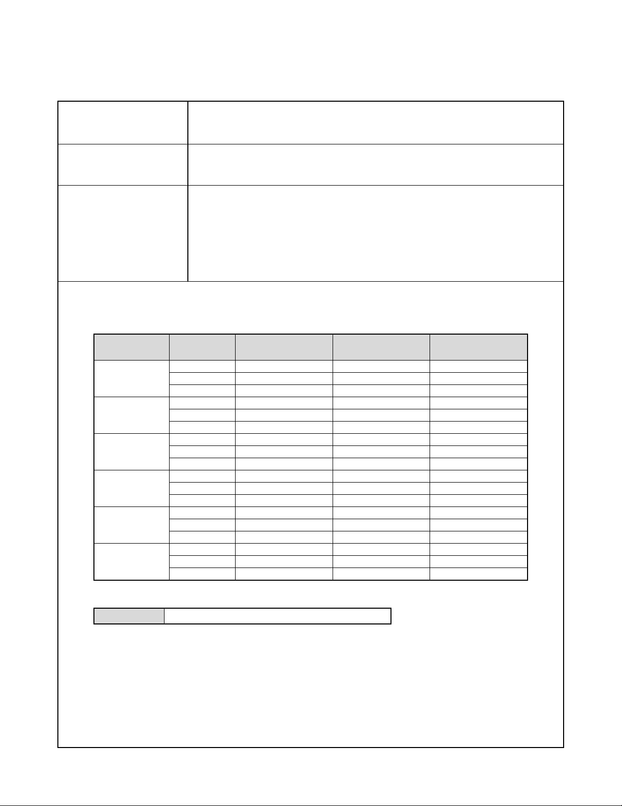
SPECIFICATIONS
■ QV-R61/QV-R62
Image Files Format Snapshots: JPEG (Exif Ver.2.2); DCF (Design rule for Camera File system) 1.0 standard;
DPOF compliant
Movies: AVI (Motion JPEG)
Recording Media 9.7 MB built-in flash memory
SD Memory Card
MultiMediaCard
Image Size Snapshots: 2816 x 2112 pixels
2816 x 1872 (3:2)pixels
2048 x 1536 pixels
1600 x 1200 pixels
1280 x 960 pixels
640 x 480 pixels
Movies: 320 x 240 pixels
Approximate Memory Capacity and File sizes
• Snapshots
File Size
(pixels)
2816 x 2112
2816 x 1872
(3:2)
2048 x 1536
1600 x 1200
(UXGA)
1280 x 960
(SXGA)
640 x 480
(VGA)
Quality
Fine
Normal
Economy
Fine
Normal
Economy
Fine
Normal
Economy
Fine
Normal
Economy
Fine
Normal
Economy
Fine
Normal
Economy
Approximate Image
File Size
2.9MB
2.3MB
1.6MB
2.7MB
2.1MB
1.4MB
1.6MB
1.2MB
630 KB
1.05MB
710KB
370KB
680KB
460KB
250KB
190KB
140KB
90KB
Built-in flash memory
9.7MB
3 shots
4 shots
5 shots
3 shots
4 shots
6 shots
5 shots
7 shots
14 shots
8 shots
12 shots
24 shots
13 shots
20 shots
35 shots
46 shots
61 shots
98 shots
SD Memory Card*
64MB
20 shots
25 shots
36 shots
22 shots
28 shots
41 shots
34 shots
45 shots
88 shots
53 shots
79 shots
154 shots
82 shots
126 shots
221 shots
294 shots
386 shots
618 shots
• Movies (320 x 240 pixels)
Data Size 300KB/second max.
* Based on Matsushita Electric Industrial Co., Ltd. products. Capacity depends on card manufacturer.
* To determine the number of images that can be stored on a memory card of a different capacity, multiply the capacities
in the table by the appropriate value.
— 1 —
Page 4

Delete Single-file, all files (with protection)
Effective Pixels 6.00 million
Imaging Element 1/1.8-inch square pixel color CCD (Total pixels: 6.37 million)
Lens/Focal Distance Seven lenses in six groups, including an aspherical lens
F2.8 (W) to 4.9 (T); f= 8 (W) to 24mm (T) (equivalent to approximately 39 (W) to 117 (T) for
35mm film)
Zoom 3X optical zoom; 4 X digital zoom
(12X in combination with optical zoom)
Focusing Contrast-type Auto Focus (AF Mode (AF Area: Spot or Multi), Macro Mode), Infinity Mode;
focus lock; manual focus
Approximate Focus Range Normal 60 cm to ∞ (infinity) (2´ to ∞)
(from lens surface) Macro Approximately 10cm to 70cm (3.9˝ to 27.6˝) at wide angle
Approximately 60cm to 70cm (23.6˝ to 27.6˝) at telephoto
Manual Wide angle: 10 cm to ∞ (infinity) (3.9˝ to ∞)
Telephoto: 60 cm to ∞ (infinity) (23.6˝ to ∞)
Exposure Control Light Metering Multi-pattern center-weighted, spot by CCD
Exposure Program AE
Exposure Compensation –2EV to +2EV (1/3EV units)
Shutter CCD electronic shutter; mechanical shutter, 1/8 to 1/2000 second (Changes in accordance
with recording mode and ISO sensitivity setting.)
• Shutter speed is different for the following BESTSHOT scenes.
Night Scene: 4 to 1/2000 second
Fireworks: 2 seconds (fixed)
Aperture Wide angle: F2.8/4.8, auto switching
Telephoto: F4.9/8.4, auto switching
White Balance Automatic, fixed (6 modes), manual switching
Sensitivity Auto, ISO64, ISO125, ISO250, ISO500
Self-timer 10 seconds, 2 seconds, Triple Self-timer
Built-in Flash Flash Modes AUTO, ON, OFF, Red eye reduction
Flash Range Wide Angle Optical Zoom: 0.6 to 2.6 meters (2.0´ to 8.5´)
Telephoto Optical Zoom: 0.6 to 2.1 meters (2.0´ to 6.9´)
(ISO Sensitivity: “Auto”)
Recording Functions Snapshot; BESTSHOT; Movie; high-speed continuous shutter mode
Monitor Screen 2.0-inch TFT color LCD
84,960 pixels (354 x 240)
Viewfinder Monitor screen and optical viewfinder
Timekeeping Functions Built-in digital quartz clock
Date and Time Recorded with image data
Auto Calendar To 2049
World Time City; Date; Time; Summer time;
162 cities in 32 time zones
Input/Output Terminals AC adaptor terminal (DC IN 3V)
USB port (Mini-B)
— 2 —
Page 5
■ QV-R61
Power Requirements
Power Requirements Two AA-size rechargeable nickel-metal hydride batteries (HR-3U <Rated Capacitance
2100mAh> and HR-3U <Rated Capacitance 2300mAh>)
Two AA-size lithium batteries
Two AA-size alkaline batteries AC adaptor (AD-C30)
Approximate Battery Life:
The values below indicate the amount of time under the conditions defined below, until power automatically turns off due to battery
failure. They do not guarantee that you will be able to achieve this level of operation. Low temperatures shorten battery life.
Operation
Number of Shots (CIPA Standard)*
(Operating Time)
Number of Shots, Continuous Recording*
(Operating Time)
Continuous Snapshot Playback*
1
3
Rechargeable Nickel-Metal
Hydride batteries
280 shots
2
(140 minutes)
900 shots
(150 minutes)
260 minutes
• The above figures are approximations only.
• The above guidelines are based on the following battery types:
Rechargeable Nickel-Metal Hydride: HR-3U (Rated Capacitance 2100 mAh) SANYO Electric Co., Ltd.
Alkaline: LR6 Matsushita Battery Industrial Co., Ltd.
• Battery life varies with brand.
• Storage Medium: SD Memory Card
*1 Number of Shots (CIPA Standard)
• Temperature: 23°C (73°F)
• Monitor screen: On
• Zoom operation between full wide to full telephoto every 30 seconds, during which two images are recorded, one image
with flash; power turned off and back on every time 10 images are recorded.
*2 Continuous Recording Conditions
• Temperature: 23°C (73°F)
• Monitor screen: On
• Flash: Off
• Image recorded every 10 seconds, alternating full wide angle and full telephoto zoom
*3 Continuous Snapshot Playback Conditions
• Temperature: 23°C (73°F)
• Scroll one image about every 10 seconds
Alkaline batteries
50 shots
(25 minutes)
245 shots
(45 minutes)
150 minutes
Power Consumption DC 3V Approximately 3.7 W
Dimensions 88.3 (W) x 60.4 (H) x 33.4 (D) mm
(3.5˝ (W) x 2.4˝ (H) x 1.3˝ (D))
(excluding projections)
Weight Approximately 168 g (5.9 oz) (excluding batteries and accessories)
Bundled Accessories Rechargeable nickel-metal hydride batteries (HR-3U <Rated Capacitance 2100 mAh>);
Charger unit (BC-5H); AC power cord; USB cable; Strap; CD-ROM; Basic Reference
— 3 —
Page 6
Rechargeable nickel-metal hydride Batteries (HR-3U) (bundled)
Rated Voltage 1.2 V
Rated Capacitance 2100 mAh
Operating Temperature
Range 0°C to 40°C (32°F to 104°F)
Dimensions 14.35 (diameter) x 50.4 (H) mm (0.56˝ (diameter) x 1.98˝ (H))
Weight Approximately 29.0 g (1.0 oz)
* Each battery
Special battery charger unit (BC-5H)
Power Requirement 100 to 240V AC, 0.08A, 50/60Hz
Output DC 1.2V, 550mA
Charging Temperature 0°C to 40°C (32°F to 104°F)
Chargeable Battery type Rechargeable nickel-metal hydride batteries (HR-3U)
Full Charge Times Approximately 4 hours
Dimensions 71 (W) x 75 (H) x 28 (D) mm (2.8˝ (W) x 30˝ (H) x 1.1˝ (D)) (excluding projections)
Weight Approximately 75 g (2.6 oz)
Power Supply
• Use only the special HR-3U rechargeable nickel-metal hydride batteries to power this camera. Use of any other type of
battery is not supported.
• This camera does not have separate batteries for the clock. The date and time settings of the camera are cleared
whenever power is totally cut off (from both the batteries and AC adaptor). Be sure to reconfigure these settings after
power is interrupted.
LCD Panel
• The LCD panel is a product of the latest LCD manufacturing technology that provides a pixel yield of 99.99%. This means
that less than 0.01% of the total pixels are defective (they do not turn on or always remain turned on).
Lens
• You may sometimes notice some distortion in certain types of images, such as a slight bend in lines that should be
straight. This is due to the characteristics of lens, and does not indicate malfunction of the camera.
— 4 —
Page 7
■ QV-R62
Power Requirements
Power Requirements Two AA-size alkaline batteries
Two AA-size rechargeable nickel-metal hydride batteries (HR-3UA <Rated Capacitance
2100mAh> and HR-3UB <Rated Capacitance 2300mAh>)
Two AA-size lithium batteries
AC adaptor (AD-C30)
Approximate Battery Life:
The values below indicate the amount of time under the conditions defined below, until power automatically turns off due to
battery failure. They do not guarantee that you will be able to achieve this level of operation. Low temperatures shorten
battery life.
Operation
Number of Shots (CIPA Standard)*
(Operating Time)
Number of Shots, Continuous Recording*
(Operating Time)
Continuous Snapshot Playback*
1
3
Rechargeable Nickel
Metal Hydride batteries
280 shots
(140minutes)
2
900 shots
(150 minutes)
260 minutes
• The above figures are approximations only.
• The above guidelines are based on the following battery types:
Alkaline: LR6 Matsushita Battery Industrial Co., Ltd.
MX1500 (AA) DURACELL ULTRA
Rechargeable Nickel-Metal Hydride:
HR-3UA (Rated Capacitance 2100 mAh) SANYO Electric Co., Ltd.
• Battery life varies with brand.
• Storage Medium: SD Memory Card
*1 Number of Shots (CIPA Standard)
• Temperature: 23°C (73°F)
• Monitor screen: On
• Zoom operation between full wide to full telephoto every 30 seconds, during which two images are recorded, one image
with flash; power turned off and back on every time 10 images are recorded.
Alkaline batteries
(LR6)
50 shots
(25 minutes)
240 shots
(40 minutes)
150 minutes
Alkaline batteries
(MX1500 (AA))
80 shots
(40 minutes)
270 shots
(45 minutes)
140 minutes
*2 Continuous Recording Conditions
• Temperature: 23°C (73°F)
• Monitor screen: On
• Flash: Off
• Image recorded every 10 seconds, alternating full wide angle and full telephoto zoom
*3 Continuous Snapshot Playback Conditions
• Temperature: 23°C (73°F)
• Scroll one image about every 10 seconds
Power Consumption DC 3V Approximately 3.7 W
Dimensions 88.3 (W) x 60.4 (H) x 33.4 (D) mm
(3.5˝ (W) x 2.4˝ (H) x 1.3˝ (D))
(excluding projections)
Weight Approximately 168 g (5.9 oz) (excluding batteries and accessories)
Bundled Accessories Alkaline batteries (LR6); USB cable; Strap; CD-ROM; Basic Reference
— 5 —
Page 8

Power Supply
• SANYO Electric Co., Ltd. brand type HR-3UA or HR-3UB batteries are recommended when using rechargeable nickel
metal hydride batteries to power this camera. Proper operation cannot be guaranteed when other batteries are used.
• This camera does not have separate batteries for the clock. The date and time settings of the camera are cleared
whenever power is totally cut off (from both the batteries and AC adaptor). Be sure to reconfigure these settings after
power is interrupted.
LCD Panel
• The LCD panel is a product of the latest LCD manufacturing technology that provides a pixel yield of 99.99%. This means
that less than 0.01% of the total pixels are defective (they do not turn on or always remain turned on).
Lens
• You may sometimes notice some distortion in certain types of images, such as a slight bend in lines that should be
straight. This is due to the characteristics of lens, and does not indicate malfunction of the camera.
— 6 —
Page 9
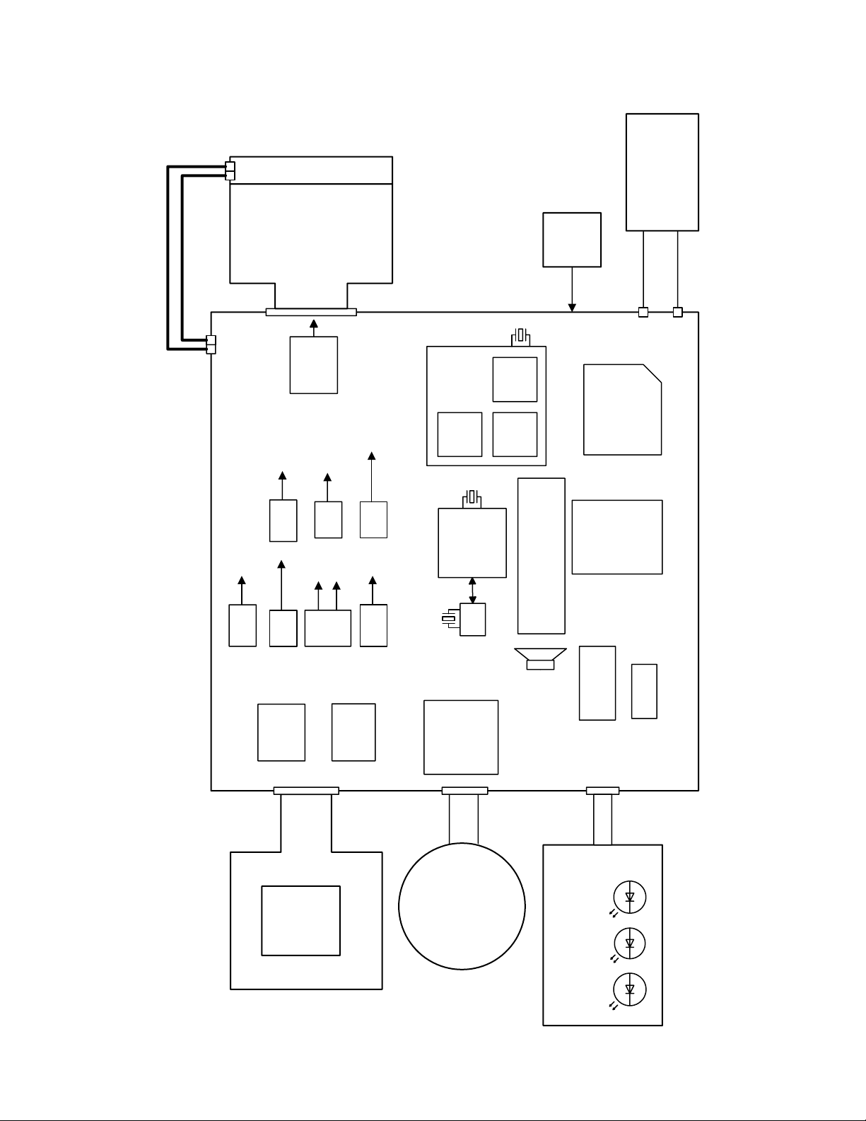
MAIN-PCB
Motor Driver
M50235HP
DOWN
Converter
VCC1.5
BACK UP
Capacitor
KONIKA
Lens Unit
×
3
SD
CCD
6Mpix
1/1.8"
15.0V
-7.5V
5.0V
C-FPC
ST-UNIT
Dry-Battery
(3.3V-2.1V)
Adapter
3.0V
20pin
22pin
VCOM
Amp
NJM2125
R
Self Timer
G
R
WIDE,TELE
21pin
SHUTTER
POWER
BUZZER
R-LEDG-LED
33pin
15V
BL (LED
×
3)
2.0" Digital I/F
LCD
VGH:15.0V
VSH:5.0V
VDD:3.0V
VCC15
VEE7.5
EVCC3.3
VCC5
VCC3.9
UP
Converter
UP
Converter
VCC3-1
VCC3-4
3.3V
1.5V
Stack MCM
M32934D4WG
13.5MHz
76C
SH
SDR
AM
8bit micon
M50235HP
4.0MHz
3.3V
32KHz
RTC
AD9949KCPZRL
3.3V
V.Driver
AN20101A
3.3V
15.0V
-7.5V
CDS
SW
RIGHT LEFT
OK UP
DOWN MENU
REC PLAY
DISP
USC Jack
FLASH RAM
TC58DAM72F1XBJ3
UP
Converter
UP
Converter
UP
Converter
UP
Converter
+
-
BLOCK DIAGRAM
— 7 —
Page 10
TEST MODE
Note: Never perform the menu items unless otherwise instructed. Doing so may cause destruction
of the data inside, which will make the camera unusable.
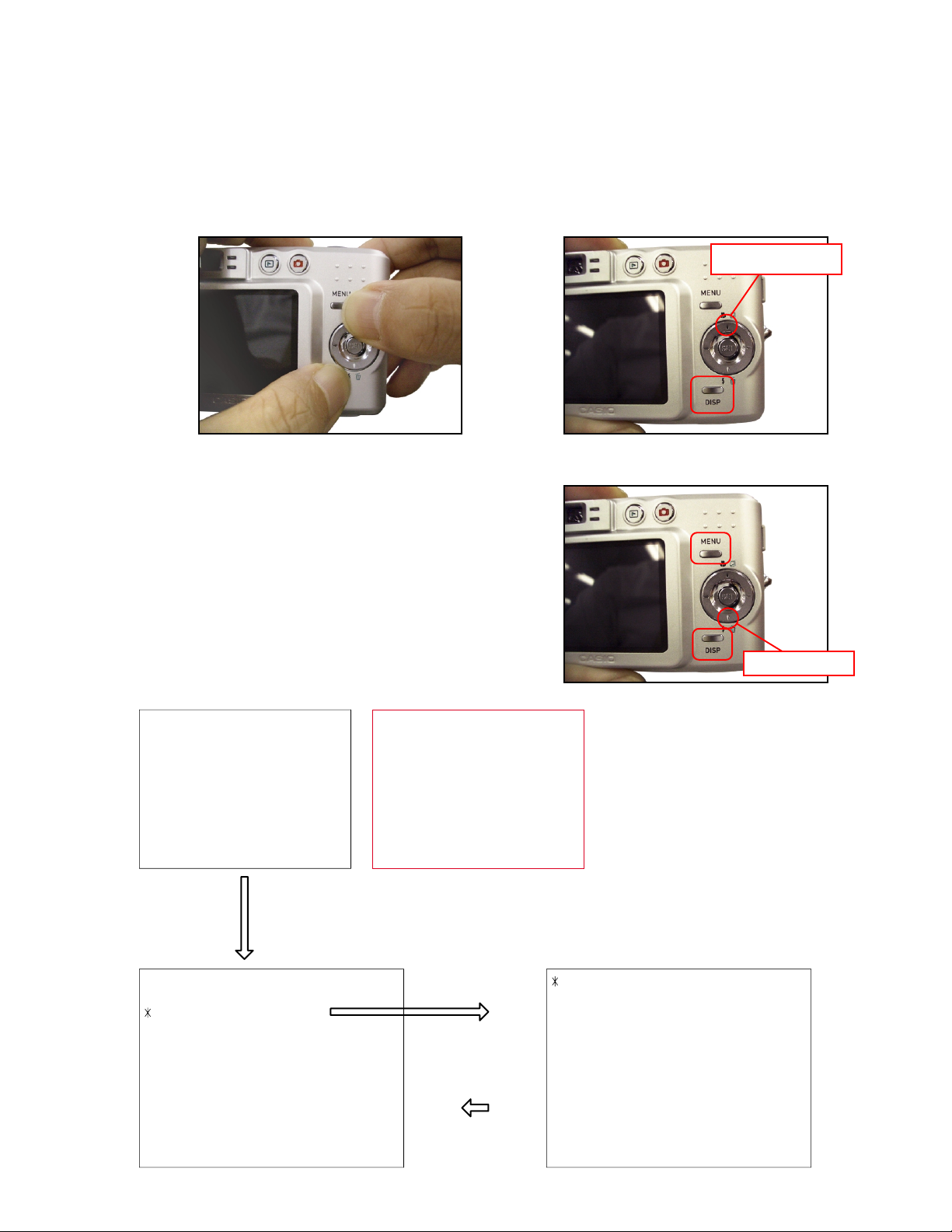
■ To boot the test mode
1. While firmly pressing down both [DISP] and [UPPER], turn the power on.
[UPPER] button
2. After the version appears, press buttons in the order of [DOWN], [DOWN], [DISP] and [MENU] in 0.5
second. The diagnostic menu appears.
■ QV-R61 ■ QV-R62
Ver 1.00
++ KX867 ++
Ver 1.00
"DOWN" button -> "DOWN" button -> "DISP" button -> "MENU" button
1 :VERSION INFO
2 :VIDEO OUT
3 :USB TCC TEST
4 :TEST MENU
5 :SOUND TEST
6 :IMAGE FLAG
7 :ROM UPDATE
8 :ADJ TEST
9 :REC-INFO
10 :TEST SCRIPT
11 :LAST MEMORY
12 :FORMAT
"SET" button
"MENU" button
[DOWN] button
++ KX813 ++
1 :USB TCC ON
2 :USB TCC OFF
3 :USB STORAGE
— 8 —
Page 11

PROGRAM VERSION UPGRADING
1. To update the firmware version
1. Prepare the memory card which contains the firmware for QV-R61/R62 in the root directory.
QV-R61.bin
QV-R62.bin
2. Insert the above memory card into the camera, and set a fully charged battery in the camera.
3. Press the [power button] while holding [MENU] depressed. Keep holding [MENU] depressed until
“PROGRAM UPDATE” appears in the display.
• The following appears.
• The version of the firmware in the memory card appears at the bottom of the display.
NOTE 1) When a wrong software is mistakenly used,
PROGRAM UPDATE
YES
NO
NEW VERSION IS
VER 1.00
(As of November 2004)
the message below appears. Update the
firmware again with the correct software.
FILE ERROR!
0x1002
NOTE 2) When only the version appears in the display
even though you are trying to operate the
camera, charge the battery to the fullest and
try again. The level of the battery indicator
should be highest in order to update the
firmware.
4. Align the white cursor to [YES] by [쑿] and [쑼], and then press [SET].
• “NOW LOADING” appears in the display and the update starts.
5. “COMPLETE” appears after the update finishes.
6. Remove the memory card after turning the power off once. Turn the power back on again while holding
[MENU] depressed, and check the version.
• “VER.1.00” appears.
VER 1.00
(As of November 2004)
7. If the version is correct, turn the power off.
8. Finally, check the operation by recording, playing back and deleting an image.
— 9 —
Page 12

2. How to restore the firmware
1. Prepare the firmware restoration program and change its name as follows;
“rom867-040913.lbn” 씮 “jupiter.bin”
“rom813-040913.lbn” 씮 “jupiter.bin”
NOTE: This software and procedure automatically restores the firmware even if the firmware belongs
to a wrong model code. Make sure to use the correct software for the correct model.
2. Copy the above file to the root directory in the memory card.
3. Insert the memory card into the camera.
4. Set a fully charged battery in the camera.
NOTE: This software and procedure automatically restores the firmware even if the battery capacity of
the camera is low. Make sure to use a fully charged battery to prevent the danger of power
down during firmware restoration.
5. Turn the power on while pressing the [shutter release] button.
If the power does not turn on only by pressing the power button, insert the battery while holding the
[shutter release] button depressed.
• The LED next to the optical viewfinder changes from “green/red blinking”, “green blinking” to “green steady”.
NOTE: This software and procedure automatically restores the firmware even if the firmware belongs
to a wrong model code. Make sure to use the correct software for the correct mode.
6. When the LED becomes “green steady”, the firmware restoration is finished.
Remove the battery and the memory card, and then turn the power off.
7. Turn the power on again while holding [DISP] and [UPPER] depressed.
Check the model name and the program version (PR:) in the opening screen of the test menu.
++KX867++
Ver 1.00
++KX813++
Ver 1.00
8. If the model name and the program version are correct, perform SYSTEM INITIAL to initialize the
system area.
“DISP+ UPPER + PW ON” 씮 “DOWN, DOWN, DISP, MENU” 씮 “7:ROM UPDATE” 씮 “5:SYSTEM
INITIAL”
NOTE: After SYSTEM INITIAL is performed, “SYSTEM ERROR” appears when the power is turned
on again.
9. Write the latest firmware.
After the firmware is written, check the model name and the program version (PR:) in the opening
screen of the test menu.
10. Finally, start the camera normally to check the operation by recording, playing back and deleting an
image. Check also that the colors in the images are not too bright or two dark.
— 10 —
Page 13

3. To install the firmware
Initially, firmware is not installed in the PCB supplied by the parts center.
Install the firmware into the PCB after replacing with a new one as shown in the procedures below.
NOTE: The camera does not operate (only LED becomes “green blinking”) if the firmware is not installed
in the PCB.
<Writing the restoration program 1>
1. Copy the following software to the root directly of the SD card.
Restoration software: rom867-040913.lbn
rom813-040913.lbn
Firmware: QV-R61.bin
QV-R62.bin
2. Change the name as follows;
“rom867-040913.lbn” to “jupiter.bin”
“rom813-040913.lbn” to “jupiter.bin”
3. Insert the SD card into the camera.
4. Insert the battery while holding the [shutter release] button depressed.
The LED next to the optical viewfinder changes from “green/red blinking”, “green blinking” to “green
steady”.
5. When the LED becomes “green steady”, remove the battery and turn the power off.
<System Initialize>
1. Boot the test mode.
2. Press [DOWN] twice and then press [DISP], [MENU].
3. Select “7: ROM UPDATE” and then press [SET].
4. Select “5: SYSTEM INITIALIZE” and then press [SET].
5. When the following message appears, press [SET].
SYSTEM INITIALIZE
START….
PUSH OK KEY?
6. The system initialize is executed. Turn off the power when “SUCCESS” appears.
* “SYSTEM ERROR” appears when the camera is turned off without system initialize.
<Writing the firmware>
1. Turn the power on while holding [MENU] depressed.
2. When “PROGRAM UPDATE” appears, select “YES” and then press [SET].
3. “NOW LOADING” appears while the firmware is updated.
4. When “COMPLETE” appears, the firmware update is complete.
5. Turn the power on and off to check if the camera normally functions. If there is no problem, the firmware
update is successful.
— 11 —
Page 14

ADJ TOOL
■ Introduction
Make sure to perform the adjustment by the USB ADJ Tool “adj03SSAW.exe” when replacing the lens
unit or the PCB.
Here the necessary software, driver and setting are explained to use “adj03SSAW.exe”.
Note that the tool, drivers etc. are available only for Windows.
1. Preparation
1-1. Prepare the necessary software, driver and DLL file.
1) Prepare the following three files.
• Common test driver for CASIO/PENTAX
[testmode_pentax_casio] folder uusbd.dll
uusbd.inf
uusbd.sys
• ADJ tool, USB DLL and ADJ setting file
[adj03SSAW] folder adj03SSAW.exe (ADJ tool itself)
uusbd.dll (USB DLL)
*.adt (ADJ setting file. Sorted by models)
* Place all files in the same folder.
2) Place the common test driver for CASIO/PENTAX in an appropriate place.
3) Place all of ADJ tool, USB DLL and ADJ setting file in the same folder.
1-2. Set the camera so that it recognizes the USB test mode.
1) Enter the test menu.
Turn the power on while pressing both [DISP] and [UPPER].
Press [DOWN], [DOWN], [DISP] and [MENU].
2) Move the cursor to “3: USB TCC TEST” and press [SET].
3) Move the cursor to “1: USB TCC ON” and press [SET].
4) The USB test mode flag is now saved in the camera. Turn the power off.
5) When the USB test mode flag is ON, the test menu appears first when the camera power is turned on.
* When turning the USB test mode flag OFF, set “2: USB TCC OFF” in the test menu.
1-3. Install the USB driver for the USB test mode in the computer.
(The following is an example using the Windows Me.)
1) Prepare the USB driver for the USB test mode.
2) Turn the camera power on which is set in the USB test mode as shown in 1-2 and let it enter the USB
test mode directly (the test menu appears right after the power is turned on).
3) Connect the camera in the above status to the computer by the USB cable.
4) The “Add new hardware” wizard appears.
5) Check “Designate the place for the driver (for users with sufficient knowledge)” and press “Next”.
6) Check “Search for the optimum driver for the device (recommended)”.
7) Check “Designate the place to search”, designate the place which contains “inf” file in the driver by
pressing “Reference” button, and then press “Next” button.
8) When “Universal USB Driver (VMEM manufacturer’s name)” appears upon message “Searching for
the driver file for the following devices”, press “Next” button.
— 12 —
Page 15

9) The file copy starts.
(If a message “uusbd.inf cannot be found” appears during the file copy, designate the same place as
in the step 7).
10) Press “Complete” button.
11) Right-click “My computer”, select “property”, and then open “Device manager”.
If “Universal USB Driver (VMEM manufacturer’s name)”,“USB device for UUSBD” can be found, the
computer has successfully recognized the driver.
12) The test driver can be used for both CASIO/PENTAX. Installing the test driver into either one enables
the other one to recognize it.
* How to uninstall the USB driver for the USB test mode
• Connect the camera to the computer while in the USB test mode so that the computer recognizes
the camera.
• Right-click “My computer”, select “Property” and open “Device manager”.
• Select “USB device for UUSBD” , and then “Universal USB Driver (VMEM manufacturer's name)”.
• Press “Delete” button to delete the driver.
• When using Windows98/98SE/Me, delete the following three files;
(NOTE! Do NOT delete “usbd.inf” and “usbd.sys”, whose names are much alike the following.)
C:windows / inf / uusbd.inf
C:windows / inf / other / KashiwanoUUSBD.inf
C:windows / system32 / drivers / uusbd.sys
• The driver has been successfully deleted.
1-4. Use the USB ADJ Tool
1) Prepare ADJ tool, USB DLL and ADJ setting file in the same folder.
2) Turn the camera power on which is set in the USB test mode and let it enter the USB test mode directly
(the test menu appears right after the power is turned on).
3) Boot “adj03SSAW.exe” and use it as follows;
• To read ADJ data from the camera
앶앸 Press “READ ($9)”.
There is no need to set the model by “FW Item Set”.
• To write ADJ data into the camera
앶앸 Press “WRITE ($8)”.
• To save ADJ data which is read
앶앸 Select “File” and “Save All ADJ”, and save it under an appropriate name.
• Open ADJ data which is saved
앶앸 1. Select the model by "FW Item Set", and then press "Load FW ->" button.
2. Select “File” and “Open”, and open the necessary file.
• Language” radio button can switch the language between Japanese and English in which the name
of the ADJ ITEM is displayed.
•“Radix” radio button can switch the data display between decimal and hexadecimal notations.
— 13 —
Page 16

2. How to use ADJ Tool when replacing Lens unit
Make sure to perform the following procedure after replacing the lens.
A floppy disk with the lens data is bundled in the spare parts of the lens unit.
1 Enter the TEST mode.
1. Turn the power on while pressing both "DISP" and "UP" buttons.
2. Press "DOWN" button, "DOWN" button, "DISP" button, and "MENU"
button while the program version is displayed.
3. Select "3.USB TCC TEST", and press "SET" button.
4. Select "1. USB TCC ON", and press "SET" button.
5. Turn the power OFF.
2 Connect the camera to the computer by the USB cable.
3 Boot "adj03ssaw" .
4 Select the model name and click "Load FW " Key.
• QV-R61 앶앸 Kx867
• QV-R62 앶앸 Kx813
5 Click "ADJ ALL READ", and display the data on the "adj03ssaw".
6 Find the No.1163, "V-COM DC".
7 Write down this value(data).
8 Replace the Lens unit.
9 Perform the above 1 to 3.
6
4
0 Select the model name and click "Load FW " Key.
• QV-R61 앶앸 Kx867
• QV-R62 앶앸 Kx867
A From "File/Open", open the bundled floppy disk, and transfer the data to
the "adj03ssaw".
B Find the No.1163,"V-COM DC"
C Change the data to the former value.(Refer to 7).
D Click "WRITE" button of "ADJ ALL".
E After adjustment, change "1. USB TCC ON" to "2. USB TCC OFF".
A
D
— 14 —
Page 17

3. How to use ADJ Tool when replacing MAIN PCB
Firmware is not installed in spare parts.
1 Enter the TEST mode.
1. Turn the power on while pressing both "DISP" and "UP" buttons.
2. Press "DOWN" button, "DOWN" button, "DISP" button and "MENU"
button while the program version is displayed.
3. Select "3.USB TCC TEST", and press "SET" button.
4. Select "1. USB TCC ON", and press "SET" button.
5. Turn the power OFF.
2 Connect the camera to the PC by the USB cable.
3 Boot "adj03ssaw".
4 Select the model name and click "Load FW " Key.
• QV-R61 앶앸 Kx867
• QV-R62 앶앸 Kx813
5 Click "ADJ ALL READ", and display the data on the "adj03ssaw".
6 Save the data.
7 Replace the MAIN PCB.
8 Writing the Firmware.
Write the firmware into a spare part after replacing one.
NOTE: If a battery is inserted without the firmware, only LED blinks
green and the camera does not operate.
9 Perform the above 1 to 3.
0 Select the model name and click "Load FW " Key.
• QV-R61 앶앸 Kx867
• QV-R62 앶앸 Kx813
A Open the file which is saved above, and display the data on the
"adj03ssaw".
B Click "WRITE" button of "ADJ ALL".
C After adjustment, change "1. USB TCC ON" to "2. USB TCC OFF".
6
5
4
A
B
— 15 —
Page 18

VCOM DC ADJUSTMENT
■ Purpose
Readjust the VCOM value to minimize the flicker of the LCD after replacing the LCD or the main PCB.
■ Necessary tools
1. Camera (Charge its battery fully)
2. Photo diode (S2281-01) : See Fig 1.
3. Photo sensor amp (C2719) : See Fig 2.
4. BNC-BNC cable (E2573) x 2 : See Fig 3.
5. 9-volt alkaline battery (6LR61Y) x 2 : See Fig 4.
6. Oscilloscope
■ Preparation
1. The three tools can be obtained from the following global site.
Photo diode (S2281-01)
Photo sensor amp (C2719)
BNC-BNC cable (E2573)
www.hamamatsu.com/
2. 9-volt alkaline battery is a standard one, but can be obtained from the following global site as well.
www.panasonic.co.jp/global/
Fig1 Photo Diode (S2281-01) Fig2 Photo Sensor Amp (C2719)
Fig3 BNC-BNC Cable (E2573) Fig4 6LR61Y
— 16 —
Page 19

■ Procedure
2:LCD
1:ADJ STAT CLR
3:LENS
.
.
.
1:VCOM OK
.
.
.
OK -> Register Write
VCOM = 0xca
This value is an example and differs by products.
Figure (a)
Figure (b)
Figure (c)
Figure (d)
1 :VERSION INFO
2 :VIDEO OUT
3 :USB TCC TEST
4 :TEST MENU
5 :SOUND TEST
6 :IMAGE FLAG
7 :ROM UPDATE
8 :ADJ TEST
9 :REC-INFO
10 :TEST SCRIPT
11 :LAST MEMORY
12 :FORMAT
1. Camera setting
a) Turn the power on while pressing “DISP” and “UPPER”.
After pressing “DOWN” key twice, press “DISP” and “MENU”.
Figure (a) appears.
b) Select “8 : ADJ_TEST” and then press SET.
(See Figure (b).)
c) Next, select “2. LCD” and then press SET.
(See Figure (c).)
2. Connecting the TOOL
d) Pressing SET causes the right figure to appear.
(See Figure (d).)
a) Place two 9-volt alkaline batteries in C2719.
b)
Connect the output terminal of C2719 to the channel terminal of the oscilloscope by the BNC-BNC cable.
c) Connect the input terminal to the Photo Diode by the BNC cable.
d) Turn the oscilloscope and C2719 on.
* Pull the ON/OFF switch of C2719 this way and raise/lower it. (See below Figure.)
— 17 —
Page 20

3. Measurement
a) Connect S2281-01 to the camera’s LCD monitor (see below).
AC Waveforms appear on the monitor screen of the oscilloscope.
* Change the Rf range of C2719 in case the range does not match.
Photo diode
S2281-01
INPUT OUTPUT
Oscilloscope
Photo sensor amp
CAMERA
BNC-BNC cable
LCD
Minimize the
ripple components
b) After AC waveforms of the oscilloscope appear, minimize it by pressing the camera’s up/down buttons
(see the picture).
Make sure to visually check if it has been minimized.
"Up" button
After it has been minimized, press SET key.
The screen in the right figure appears and the new VCOM
is written (VCOM adjustment is finished.).
Return to the previous display by pressing MENU or PW key.
"Down" button
OK -> Register Write
VCOM = 0xca
ADJ DATA SET!
This value is only an example, and differs by products.
— 18 —
Page 21

CURRENT CONSUMPTION
(1) Current consumption (DC in = 3.00 ± 0.05 [V])
• Make sure that current consumption is less than 429 mA in PLAY mode.
• Make sure that current consumption is less than 657 mA in REC mode.
• Make sure that current consumption is less than 1.3 mA when power is turned OFF.
(2) The battery indicator changes according to the voltages as follows.
• DC in = less than 2.43 ± 0.02V: (PLAY mode)
• DC in = less than 2.38 ± 0.02V: (PLAY mode)
• DC in = less than 2.21 ± 0.02V: (PLAY mode)
THE COUNTERMEASURE FOR "SYSTEM ERROR"
System error may occur when the battery is removed while data is written to the internal memory.
■ PROCEDURE
1. Initialize the system.
a) Enter the TEST mode.
b) Select "7:ROM UPDATE" and press SET button.
c) Next, select "5:SYSTEM INITIAL" and press SET button.
d) The following message appears.
SYSTEM INITIALIZE
START
PUSH OK KEY?
e) Press SET button and System is initialized.
"SUCCESS !" appears on the monitor.
2. Write firmware.
Refer to the "1. To update the firmware version" on page 7.
Write the firmware.
If the TEST mode boots automatically, change "USB TCC ON" to "USB TCC OFF".
Replace the Main PCB if the camera does not recover.
...
— 19 —
Page 22

DISASSEMBLY
■ There are several types of screws. Make sure to use the
correct ones.
■ It is a good idea to sort them as shown in the figure when
disassembling.
1. Remove the batteries.
■ Removing the rear panel
2. Remove six screws.
Screws (S3)
Screws (S4)
3. Remove the rear panel.
4. Remove the connector cover and the AC jack cover.
Screws (S2)
Screws (S3)
AC jack cover
Rear panel
Connector cover
— 20 —
Page 23

5. Remove one screw (S1) and then the strap board.
Screw (S1)
■ Removing the front panel unit
6. Remove two screws (S2).
Strap board
Screws (S2)
7. Unsolder two battery plates.
Battery plates
8.
While opening the case in the direction of the arrow, remove the electronic block from the front panel unit.
NOTE: Make sure that the hooks are snapped
together when assembling.
Hooks
— 21 —
Page 24

NOTE: Make sure to discharge the strobe condenser when removing the front panel.
■ Disassembling the front panel unit
9. Remove two screws (S3) and then remove the tripod sock.
Screws (S3)
10. Remove four screws (S5) and then remove the cam ring and the upper case.
Screws (S5)
Screws (S5)
Cam ring
11. Remove two screws (S2) and then remove the center case.
Tripod sock
Upper case
Center case
Screws (S2)
— 22 —
Page 25

■ Removing the LCD
12. Lift the LCD unit by a pair of tweezers and then remove the LCD unit from the LCD frame.
LCD frame
Concave part
Channel
13. Unsolder the two lead wires.
14. Remove the connector.
15. Remove the LCD unit.
Connector
NOTE: Make sure to insert the connector tightly
when assembling, or the display will be
defective.
Red cord
Black cord
16. Remove three screws and then remove LCD frame.
screws
screws
— 23 —
Page 26

■ Removing the PCB
17. While heating the upper part of the earth board by a soldering iron, lift up the earth board by a pair of
tweezers and remove it.
Earth board
NOTE: Temporarily fixing the earth board by a screw
makes it easier to solder when assembling.
18. Remove the connector.
19. Remove one screw (S7).
20. Remove the connector.
Clamp board
Screw (S7)
— 24 —
Page 27

21. Remove the PCB
■ Disassembling the battery case
22. Remove one screw (S8) and then remove the battery case.
Screw (S8)
PCB
Battery case
23. Remove one screw (S9) and then disassemble the battery case (See the figures below for the position of
the hooks).
Screw (S9)
Battery cover
— 25 —
Page 28

■ Removing the lens unit
24. Remove two screws (S10) and then remove the lens unit.
Strobe unit
Screws (S10)
(with CAPA holder)
Lens unit
NOTE: Insert the convex portion into the concave portion tightly as shown in the figures below
when assembling.
B
Insert A into B tightly.
A
D
Insert C into D tightly.
C
— 26 —
Page 29

EXPLODED VIEW
S2
S1
S2
11
10
4
5
14
15
7
9
8
S2
6
3
17
2
1
16
12
S3
13
S2
18
S3
S4
S3 S3
19
21 20
22
— 27 —
Page 30

PARTS LIST
■
QV-R61
Price
N Item Parts Code Parts Name Specification QTY
N 1 10174881 PCB ASSY/MAIN TK-RJK506801*001 1 DT A
2 10127443 COVER/JACK RJK504662-001V01 1 AE C
3 10126467 STRAP BOARD RJK504626-001V01 1 AK X
4 10147342 STROBE UNIT XEST-K865-1-ST 1 CN C
5 10135336 EARTH BOARD RJK504747-001V01 1 AA X
N 6 10174885 BOX ASSY/BATTERY TK-RJK506807*001 1 EF C
N 7 10174880 LENS UNIT TK-RJK506799*001 1 ED A FD attached
N 8 10174888 CASE ASSY/UPPER TK-RJK506811*001 1 AE C
N 9 10174889 PANEL ASSY/FRONT TK-RJK506812*001 1 BV C
N 10 10175831 GRIP RJK505463-003V01 1 AK C
N 11 10152188 TAPE RJK506125-001V01 1 AA C
N 12 10174835 CAM RING RJK504660-005V02 1 BQ C
13 10126478 TRIPOD SOCK RJK504763-001V01 1 AM C
N 14 10174887 CASE ASSY/CENTER TK-RJK506810*001 1 BK B
15 10127445 COVER/CONNECTER RJK504663-001V01 1 AE C
16 10127436 HOLDER/CAPA RJK504693-001V01 1 AB X
N 17 10174886 COVER ASSY/BATTERY TK-RJK506809*001 1 AT C
N 18 10174883 PANEL ASSY/REAR TK-RJK506803*001 1 CG C
N 19 10174806 LABEL/RATING RJK504669-010V01 1 AA C For EU/US
N 19 10174815 LABEL/RATING RJK504669-011V01 1 AA C Except EU/US
N 20 10174882 LCD ASSY TK-RJK506802*001 1 DH B
21 10153672 SUPPORT/LCD RJK505467-001V01 1 AA X
22 10153671 FRAME/LCD RJK505466-001V01 1 AB X
S1 10086282 SCREW RJK502970-001V01 1 AA X
S2 10086285 SCREW RJK502971-001V01 5 AA X
S3 10131119 SCREW RJK502970-004V01 5 AA X
S4 10086284 SCREW RJK502970-003V01 2 AA X
FU100 10128794 FUSE FCC10162ABPA 1 AA A
FU101,FU102 10128795 FUSE FCC10132ABPA 2 AA B
FU103 10175616 FUSE ERBSD0R50U 1 AA B
Code
R Remark
ACCESSORY
N - 10175035 CD ROM CK867DCA01R 1 AF C
- 10090421 USB CABLE UC-K861-LG10 1 AQ C
- 10136903 AC CORD CBL-K864-AC-JU 1 AI C Blade type
- 10136905 AC CORD CBL-K864-AC-EU 1 AJ C EU type
- 10136906 AC CORD CBL-K864-AC-UK 1 AX C UK type
- 10126486 CHARGER NC-MDR01JUCA 1 BV C *1
- 10126488 CHARGER NC-MDR01WCA 1 BV C *2
- 10127402 BATTERY/NI-MH HR-3U-KSO-4E 2 AR B
- 10090412 STRAP ST-K861 1 AF X
New parts.
N:
*1 Blade type AC cord is bulit-in.
*2 AC cord is not built-in.
— 28 —
Page 31

■
QV-R62
N Item Parts Code Parts Name Specification QTY
1 10174881 PCB ASSY/MAIN TK-RJK506801*001
2 10127443 COVER/JACK RJK504662-001V01
3 10126467 STRAP BOARD RJK504626-001V01
4
5 10135336 EARTH BOARD RJK504747-001V01
6 10174885 BOX ASSY/BATTERY TK-RJK506807*001
7 10174880 LENS UNIT TK-RJK506799*001
8 10174888 CASE ASSY/UPPER TK-RJK506811*001
9 10174889 PANEL ASSY/FRONT TK-RJK506812*001
10 10175831 GRIP RJK505463-003V01
11 10152188 TAPE RJK506125-001V01
N 12 1018 1494 CAM RING RJK504660-007V02
13 10126478 TRIPOD SOCK RJK504763-001V01
N 14 1018 1966 CASE ASSY/CENTER TK-RJK506810*003
15 10127445 COVER/CONNECTER RJK504663-001V01
16 10127436 HOLDER/CAPA RJK504693-001V01
17 10174886 COVER ASSY/BATTERY TK-RJK506809*001
18 10174883 PANEL ASSY/REAR TK-RJK506803*001
N 19 1018 1471 LABEL/RATING RJK504669-018V01
N 19 1018 1472 LABEL/RATING RJK504669-019V01
20 10174882 LCD ASSY TK-RJK506802*001
21 10153672 SUPPORT/LCD RJK505467-001V01
22 10153671 FRAME/LCD RJK505466-001V01
S1 10086282 SCREW RJK502970-001V01
S2 10086285 SCREW RJK502971-001V01
S3 10131119 SCREW RJK502970-004V01
S4 10086284 SCREW RJK502970-003V01
FU100 10128794 FUSE FCC10162ABPA 1 AA A
FU101,FU102 10128795 FUSE FCC10132ABPA 2 AA B
FU103 10175616 FUSE ERBSD0R50U 1 AA B
10147342
STROBE UNIT
XEST-K865-1-ST 1
1
1
1
1
1
1
1
1
1
1
1
1
1
1
1
1
1
1
1
1
1
1
1
5
5
2
Price
R Remark
Code
DT A
AE C
AK X
CN C
AA X
BC C
ED A FD attached
AE C
BV C
AK C
AA C
BC C
AM C
BU B
AE C
AB X
AT C
CG C
AA C For EU/US
AA C Except EU/US
DH B
AA X
AB X
AA X
AA X
AA X
AA X
ACCESSORY
N - 1018 1704 CD ROM CK813DCA01R 1 AE C
- 10090421 USB CABLE UC-K861-LG10 1 AQ C
1018 1159 BATTERY/ALKALINE LR6GW/2ST 1 AE B 1set : 2pcs
- 10090412 STRAP ST-K861 1 AF X
N: New parts.
— 29 —
Page 32

MAIN PCB (TOP VIEW)
PRINTED CIRCUIT BOARDS
— 30 —
Page 33

MAIN PCB (BOTTOM VIEW)
— 31 —
Page 34

SCHEMATIC DIAGRAMS
MAIN PCB (1/2)
VCC1.5
VCC1.8
VCC3-1
L401
L403
L402
HW680
HW680
HW680
B10u
2012
2012
B10u
2012
B10u
C409
6.3V
6.3V
C408
6.3V
C406
OPEN
C427
1
2
3
X401 48.0MHz
C428
R427
CCR48.0MXC7A15T
OPEN
100
TGND
GRM1552C1H9R0DZ01D
C420
CH9p
14
32
C419 CH9p
R424
1.5k
X400 27MHz
GRM1552C1H9R0DZ01D
FCX-04-CWDS270A
TGND
SYS-BUS
SYS-BUS[6]
S-AND
FLASH ROM
TEST
MODE1
MODE2
MODE3
MRES_B
VCC3.3D
VCC1.8D
VCC1.5D
P425
LCDD2
LCDD3
LCDD4
LCDD5
LCDD6
LCD-BUS
LCDD7
VBUS
SD-BUSSD-BUS
DMINUS
DPLUS
RESETB
R426
OPEN
WKUPB
STBYB
1M
R418
PSRSTB
LCD-BUS
SYS-BUS
LCDCTL
LPWM
NAND
L
L
L
L
H
H
LH
OPEN
H
LCD-BUS
STB
CLK
GSRT
VCC3.3D VCC3.3D
VCC1.8D VCC1.8D VCC1.8D VCC1.8D
VCC1.5D VCC1.5D VCC1.5D VCC1.5D
297
298
299
300
301
P141
P152
P143
302
P140
303
VSSQ_16
LD_DAT2
304
LD_DAT3
305
VSS_18
306
LD_DAT4
307
LD_DAT5
308
LD_DAT6
309
BSEL2#
310
READY#
311
LD_DAT7
312
A12
313
A11
314
C404
A10
315
B0.1u
VCC_7
316
A13
317
A14
318
A15
319
VCC1.8DVCC1.8DVCC1.8D
VCC1.5DVCC1.5DVCC1.5D
VCC3.3DVCC3.3DVCC3.3D
VSS_19
320
VDDQ_15
321
A18
322
A17
323
A16
324
VCCX1_9
325
VSSQ_17
326
A19
327
A20
328
A21
329
VSS_20
330
VDD_20
331
A24
332
A23
333
A22
334
VCCX1_10
335
VSS_SD_19
336
A25
337
A26
338
A27
339
VSS_21
340
VDDQ_16
341
A30
342
A29
343
A28
344
VCCX1_11
345
VSSQ_18
346
DCS1#
347
DCKE
348
VCCX1_12
349
VSS_F_2
350
VDD_21
351
NC
352
VBUS
353
BSEL0#
354
FVCC_2
355
VSS_SD_20
356
P406
TCK
357
P401
C400
TDI
358
B0.1u
VCCX1_13
359
C402
VSS_22
360
B0.1u
VDDQ_17
361
DM
362
P405
TMS
363
R413
TRST#
0
364
VCCX1_14
365
VSSQ_19
366
DP
367
C401
RST#
B0.1u
368
P402
TDO
369
C405
VSS_F_3
370
B0.1u
VDD_22
371
USBXIN
372
TEST
373
MODE1
374
VCCX1_15
375
VSS_SD_21
376
USBXOUT
377
WKUP#
378
MODE2
379
VSS_23
380
VDDQ_18
381
XIN
R425
382
DBI#
383
0
STBY#
384
VCCX1_16
385
VSSQ_20
386
XOUT
387
SBI#
388
P070
389
VSS_24
390
VSS_SD_22
391
P073
392
P072
393
P071
394
VCC_8
395
P074
396
P075
397
TRDATA0
398
TRDATA3
399
TRDATA2
400
TRDATA4
401
DUMMY
VSS_12TRSYNCX3TRDATA54TRDATA75TRDATA6
1
VCC1.5D VCC1.5D
VCC1.8D VCC1.8D VCC1.8D
VCC3.3D VCC3.3D VCC3.3D
CP
STH
FRP
GRES
GPCK
OPEN
R408
0
R409
291
292
293
294
295
296
P151
P150
P142
MODE3
VDDQ_14
VSS_SD_18
TRDATA17EVENT08EVENT19P01010VDDQ_111P01312P01213P01114VCCX1_115VDD_116P01417P01518P01619VSS_220VSS_SD_121P07722P07623P01724VCCX2_126P04027P04128P04229VSS_330VDD_231P04532P04433P04334VCCX2_235VSS_SD_236RTCCLKIN37P04638P04739VSS_440VDDQ_241CD_ADCLK42P03643P03544VCC_145VSSQ_246TRCLK47P03748VDDQ_349VSSQ_350VDD_351P06152P060
6
POL
B0.1u
C410
276
277
278
279
280
281
282
283
284
285
286
287
288
289
290
CAS#
P147
P146
RAS#
VSS_17
VDD_19
C407
B0.1u
VSSQ_15
P027
P026
DWE#
P145
P144
VDDQ_13
VCCX1_8
VSS_SD_17
SELFLED
RLED
GLED
BLCTL
SYS-BUS
PSCK
C411
B0.1u
265
266
267
268
269
270
271
272
273
274
275
PRE
P023
P022
P025
P024
P155
VSS_SD_16
VSSQ_1
25
SYSCLK
VSS_16
VDD_18
VCCX1_7
A
D
C
B
296
25
305
303
300
297
304
306
24
301
307
298
308
302
23
299
311
309
310
22 199
315
314
312
313
21
318
317
319
316
20
323
322
324
321
19
327
18
329
328
326
331
17
333
332
334
338
16
336
339
337
344
343
342
341
14
347
346
349
348
351
13
354
352
353
356
359
357
12
358
362
364
361
11
363
369
368
10N366
367
9
372
373
371
374
376
8
379
378
377
7
384
381
383
382
6
387
386
389388
5
393
394
391
392
10
396
397
395
9
3
399
398
3
2
5
8
400
1
7
4
1
2
D
C
A
22k
R455
CENDN
CHG
WATCH
PSIN
PSOUT
BCOVER
TRON
KINTB
C414
C412
B0.1u
B0.1u
252
253
254
255
256
257
258
259
260
261
262
263
264
DQM1
P021
VCC_6
VSSQ_14
E
F
291 266
286K276
287
292
288
293
294
289
290
295
320
325
330 177
335
340
345
350
355
360
365
370
375
380
385
390
401
15
20
19
14
13
18
17
12
16
11
E
F
C413
Strobe-BUS
SD-BUS
FOUT
LCD-BUS
TRON
P020
P007
DQM0
VDD_17
VSS_15
VCCX1_6
VDDQ_12
VSS_SD_15
H
J
K
G
271
281
261
267
277
282
272
278
273
268
283 201218
269 219
274
264
279
280
275
265
270
285
IC400
R8J30205BG-E
40
30
35
25
39
34
24
29
38
33
28
23
32
27
37
22
26
36
31
21
JAA
G
H
0
B0.1u
R428
ADCLK
CCD-BUS
IGBTG
SDCLK
SYS-BUS
BEND3
SHUTTER2
VCC3.3DVCC3.3D
243
244
245
246
247
248
249
250
251
CS#
P003
P005
DSE#
P006
VCC_5
DCS0#
VDD_16
VSSQ_12
VSSQ_13
R
N
M
L
P
246
241
251
256
252
257
242
247
262
258
263
243
253
248
244
249284
259
254
255
250
245
260 230
55
50
65
60
45
49
59
54
64
44
58
63
53
48
43
52
47
62
42
61
56
46
51
41
M
R
P
L
VSS_SD_354VDD_455VSS_SD_456P06257P06358VCCX2_359VSS_560VDDQ_461P06662P06563P06464VCC_2
53
SDCMD
SDDAT0
SDDAT1
SDDAT2
ZOOM_ENCO
C415
R430 100k
235
236
237
238
239
240
241
242
P002
P001
P004
AVREF
VSS_14
USBVSS
VDDQ_11
VSS_SD_14
U
W
T
V
226
221
231
236
237 204
232
227
222
223
228
238
233
239
224
234
229
225
235
240
80
85
75
70
84
794
74 89
69
78
73
68 83
82
6757
72
77
66
76 91
81
71
W B
V
T
U
VSSQ_466P06767P05068P05169VCCX1_270VDD_571P05472P05373P05274VDD_675VSS_SD_576P055
65
VCC1.5D
SDDAT3
SDWP
PWCTL0-2
PSRDY
LENS_TH
0
R417
C416
B0.1u
229
230
231
232
233
234
AN3
AN2
P000
VDD_15
AVCC_3
Y
AB
216
209
212
217
213 203
210
211
214
215
195
220
194
190
189
185
184
180
179
174
175
170
169
16515
164
159
160
155
154
150
149
145
144
140
139
135
134
129
130
125
124
119
120
90
115
95
99
94
936
88
98
92
97
87
96
86
AB
Y
ZOOM_LED
FOCUS_LED
MD-BUS
SDDET
ZOOM_HOME
FOCUS_HOME
B0.1u
10k
R407
225
226
227
228
224
AN0
AN1
ADTRG
AVSS_3
VSSQ_11
AEAA
AC
AD
205
206
207
208
202
200
198
197
196
193
192
191
186
187
188
182
181
183
178
176
172
171
173
168
166
167
163
161
162
158
157
156
152
153
151
147
146
148
143
142
141
136
138
137
131
133
132
126
128
127
121
123
122
116
118
117
113
112
114
109
111
110
102
107
108
104
106
101
100
105
103
AC
AD
VCC3.3D
ENC_LED
SHUTDLY
Strobe-BUS
CD7
CD9
CD8
CD10
CD11
R410
F3.3k
214
215
216
217
218
219
220
221
222
223
AIREF
AVCC_1
AVOUTB
AVSS_2
VDD_14
AVCC_2
CD_DAT9
CD_DAT8
CD_DAT10
CD_DAT11
25
24
23
22
21
20
19
18
17
16
15
14
13
12
11
10
9
8
7
6
5
4
3
2
1
AE
P05678P05779VSS_SD_680VDDQ_581P03282P03183P03084VDDQ_685VSSQ_586P03387P03488P120
77
C417
B0.1u
VCC3-0
L420
BK2125HS101-T
TGND
CD4
CD5
CD6
CD1
P400
B1u
B1u
C421
C418
VIDEO
220
R406
213
207
208
209
210
211
212
AVGA
AVGB
P080
AVOUT
CD_DAT6
CD_DAT7
CD_DAT4
CD_DAT5
VSSQ_690VDD_791P12392P12293P12194VDD_895VSS_SD_796P12497P12598P12699VSS_SD_8
89
FOCUS1
FOCUS0
FOCUS2
FOCUS3
IC421
C140
R1230D151F-TR-FA
B10u
1
VIN
2
PGND
3
VDD
4
CE
1M
R429
VCC1.5
CCD-BUSCCD-BUS
MD-BUSMD-BUS
SYS-BUSSYS-BUS SYS-BUS
CD2
CD0
CD3
CDSHD
B1u
C422
201
202
203
204
205
206
AVR
P082
P081
P083
VSS_13
CD_DAT2
CD_DAT3
AVSS_1
P086
P085
P084
VSS_SD_13
VCC_4
P087
P090
P091
VDD_13
VSS_12
P094
P093
P092
VSSQ_10
VDD_12
P095
P096
DSC#
VDDQ_10
VSS_SD_12
P100
P097
MRES#
VSS_SD_11
VCCX1_5
P101
P102
R/B#
VDD_11
VSS_11
P104
P103
RS#
VSSQ_9
VCCX1_4
P105
P106
FCE#
VDDQ_9
VSS_10
VCCX1_3
P107
SACE#
VSS_SD_10
FVCC_1
P110
D1
D0
VDD_10
VSS_F_1
VCCX3_2
D2
D3
VSSQ_8
VCCX3_1
CDE
D5
D4
VDDQ_8
VSS_9
ALE
D6
D7
VSS_SD_9
VCCX2_5
P111
D9
D8
VDD_9
VSS_8
WP#
D10
D11
VSSQ_7
VCCX2_4
P112
D13
D12
VDDQ_7
VSS_7
P113
D14
D15
VCC_3
P116
P115
P114
P117
P154
P137
P134
P136
P135
VSS_6
P133
P132
P127
P130
P131
100
IRIS1
FOCUS4
FOCUS5
L421
8
LX
7
10u
AGND
6
MODE
5
VOUT
VCC1.8DVCC1.8DVCC1.8D
VCC1.5DVCC1.5DVCC1.5D
200
199
198
197
196
1
2
195
C423
B0.1u
194
193
192
191
190
189
188
187
186
185
184
183
182
181
180
179
178
177
176
175
174
173
172
171
170
169
168
167
166
165
164
163
162
161
160
159
158
157
156
155
154
153
152
151
150
149
148
147
146
145
144
143
142
141
140
139
138
137
136
135
134
133
132
131
130
129
128
127
126
125
124
123
122
121
120
119
118
117
116
115
114
113
112
111
110
109
108
107
106
105
104
103
102
101
TGND
C431
6.3V47u
R412
5.1k
2
C425
B0.1u
C424
B0.1u
1
VCC1.5
SY8-0J476M-RA
1
2
P407
G-short
VCC3.3DVCC3.3D VCC3.3D
1
2
GND
MD-BUS
VCC3-1
R431
0
TGND
C433
B1u
C435
XC6219B182MR
100k
CD_SHUTM
CD_SHUT
MT_DCPLS
ZOOM1
ZOOM0
IRIS0
IC422
1
VIN
VOUT
2
VSS
3
CE
NC
VCC1.8
CCD-BUS
MD-BUS
CDSVD
CDSCS
CDSDT
CDSCK
CCD-BUSCCD-BUS
XSUB
OFDC
CH3
CH2
CH1
CH4
CH5
MD-BUS
XV1
XV3
XV2
XV4
XV5
XV6
MD-BUS
CCD-BUS
P430
VCC1.8
5
4
B1u
C434
SYS-BUSSYS-BUS
SYS-BUS
SD-BUSSD-BUSSD-BUS
CCD-BUS[33]
MD-BUS[21]
SELFLED
IGBTG
CHG
CENDN
Strobe-BUS
RLED
GLED
Strobe-BUS
EVCC3.3
R479
SYS-BUS
F91k
4
4
REC
PLAY
SW461 LS8J3M-T
SW460 LS8J3M-T
123
123
R478
F13k
GND
R477
F560
VCC1-1
R476
1K
R420
C450
R448
F82k
KIN2
KIN1
KIN3
R449
C445
F300k
B0.1u
P470
C466
B0.1u
EVCC3.3
EVCC3.3
IC441
R457
75S58
R419
F82k
1
2
F36k
3
C481
B0.1u
B0.1u
REC/PLAY
R454
R453
F10k
100k
5
-
VDD
R468
VSS
OPEN
4
+
OUT
C449
B0.1u
TGND
0
R456
C447
B0.1u
F10k
R470
F10k
TGND
VCC3-2
R451
100k
BCOVER
SD-BUSSD-BUS
IC452
S-80820CNNB
SYS-BUS
PWSW
SDDAT3
SDCMD
SDCLK
SDDAT0
SDDAT1
SDDAT2
SDDET
SDWP
VBUS
R415
F24
DMINUS
R416
F24
DPLUS
R414
1.5k
TRON
VCC1-ST
VCC5-1
54722-0207
1
IGBTG
2
VCC5-1
3
CHG
4
PWSW
5
CENDN
6
VCC1-ST
7
VCC1-ST
8
NC
9
RLED
10
GLED
VCC3-2
L48010u
GLF2012T100K
C480
6.3V47u
BUZZER
SI1012X
EVCC3.3
VCC15L
to_strobe_FPC
3
1
D
12
+
-
D480
2
MA27728
TGND
SP480
NFT-03A
18
P121
R480
Q480
3
P480
1
2
TGND
TGND
R433
100k
USBCONB
3
Q434
R635
DTC144EE
510
1
2
TGND
L452
ACM2012-900-2P
TGND
VCC15
VCC5-1
L630
100u
SI1013R
L620
Q621
2
3
100u
R621
1M
1
R620
100k
Q620
3
LGND
DTC144EE
1
2
LGND
L450
HS601
L451
HS601
CN452
P122
14
23
C620
B10u
EVCC3.3
SELFLED
GND
GND
GND
GND
GND
SHUTSW1B
SHUTSW2B
KIN3
R400 47k
R401 47k
CN453 USB
54819-1572
1
2
3
4
5
P450
USB_CASE
VCC15L
VCC5L
LGND
LCD-BUS[17]
BLCTL
GND(COM)
EVCC3.3
11
12
13
14
15
16
17
18
19
20
GND
10
DET
11
12
WP
GLF2012T100K
R402 47k
R403 47k
R404 47k
R405 10k
R491 HW680
C430
B1u
R493 HW680
R494 HW680
R495 HW680
R496 HW680
TGND
USBVCC
DMINUS
DPLUS
ID
UGND
Q623
EMX2
R632
1
D110
R633
D5.1k
3
R634
D1.3k
R469
F43k
R485
F82k
C467
B0.1u
PSIN
GRM31CB30J476ME18L
R467
F13k
3
4
SHUTSW1B
SHUTSW2B
SW_ON
SW_OFF
SW_ON
SW_OFF
VCC3-1
L430
10u
R492 0
R497 0
R498 0
1k
R483
LGND
R602
F4.7k R603
FRP
6
542
IC461
75S58
1
-
2
VSS
3
+
PWCTL2
49
50
51
52
53
54
55
56
57
58
59
60
61
62
63
64
R458
100k
R459
100k
PSCK
C451
B47u
R450
F300k
VDD2NC
OUT
VSS
KIN3
to SD
1
2
3
4
5
6
7
8
9
10
11
12
13
SCDA1A1301
1
2
3
IC601
TC7SZ32AFE
VCC5L
36k
R604
36k
R605
VCC15
EVCC3.3
5
VDD
4
OUT
C468
TGND
SYS-BUS
48
VREF
AVDD
10
P16
9
AD1
8
AD0
7
AD3
AD2
6
AD5
5
AD4
AD7
4
AD6
3
AD9
AD8
2
P20
1
AVSS
P22
RESETB
VCC1-1
R452
F68k
R446
0
1
C454
OPEN
TGND
CN451
DAT3
CMD
VSS1
VDD
CLK
VSS2
DAT0
DAT1
DAT2
DET
GND1
WP
GND2
5
4
IC600
NJM2125F
1
+
V+
2
V-
3
-
OUT
F8.2k
BLLEDA
P403
P404
BLLEDK
B0.1u
PWCTL0
PWCTL1
49
50
54
58
62
64
P231P242P213P254P265P276P307P318P32
PSOUT
SYS-BUS
VCC15L
5
4
KINTB
PSRDY
SHUTSW2B
R465
R471
100k
100k
40
45
P1546P1447P17
515247
53
55
57
59
61
63
3
2
BJ
STBYB
EVCC3.3
B2700p
P12
4620385642
5
4
C453
C603
B1u
C601
B10u
VCC5L
44
45141
ML610501
7
6
C
WATCH
R622
F20k
1
R626
F62k
P1043P13
LPWM
42
IC440
SHUTTER2
R600
43
92713
8
E
10k
C600
P0641P11
SHUTSW1B
BEND3
B0.1u
3
2
36
39
P07
P0237P0538P04
36
40
344448
39
35DA37
31
29
25
23
21
15
11
19
12
14
16
10
H60G
F
I
P33
P34
P36
P35
9
12
10
11
13
EVCC3.3
SYS-BUS
D630
RB521S-30
VCC15L
R630 10
VCC5L
3
1
Q600
2
2SD2216J-R
VCOM_DC
8.2k
470 R606
R601
LGND
D2k
R623
R624
D16k
Q622
2SD2216J-R
D2k
R625
PSRSTB
14
ADPTN
SW440 LS8J2M
R440
SW441 SKRKEE010SW442 SKRKEE010
R441
R442
EVCC3.3
32KHz
X460
CK1p
C461
TFX-01-AWAS327A
GRM1554C1H1R0CZ01D
R463
OPEN
12
CK1p
R460
100k
C446
B0.1u
C448
B0.1u
TGND
4
RIGHT
4
DOWN
C444
NC
VSS
VC2
NC
VDD
GRES
GSRT
VCOM
STBYB
POL
CLK
D04
D02
D00
VSS
VRH
VDD
GND
R461
6.8k
1
P441
C442
TGND
P440
C443
B0.1u
GND
B0.1u
TGND
R462
6.8k
C460
B0.1u
Q441
DTC144EETL
1
KIN1
B0.1u
KIN2
KIN3
CN600
54393-3382
C462
GRM1554C1H1R0CZ01D
10
CIN
11
VSS
12
/VDCC
VCC3-1
TGND
SYS-BUS
NC
VC1
VGL
VGH
CP
GPCK
STBYB
STH
RIT
STB
D05
D03
D01
VSH
VBC
VRL
3.9k
3
2
PWSW
WKUPB
R472
100k
33
P47
P0134P0035P03
32
P46
31
33
P45
30
P44
32
29
P43
30
28
P42
27
28
P41
26
P40
26
25
VDDL_2
24
24
VSS
23
VDDL_1
22
RESETB
XT1
18
XT0
TEST1B
17
TEST0B
OSC0
P37
P50
OSC1
15
16
4
OK
123
F560
MENU
F560
DISP
F560
R486
OPEN
22
P442
21
20
19
R473 0
18
R474 0
17
3
3
1
2
Q442
DTA114EE
X440
2
CSTCE10M
4
LEFT
SW443 LS8J2M
SW446 LS8J2M
123
123
R445
F11k
R443
F3.9k
4
UP
SW444 LS8J2M
SW447 LS8J2M
123
123
R447
F11k
R444
F3.9k
to_LCD
C631
B1u
C630
B1u
12
C632
B1u
GRES
GSRT
P123
VCOM
POL
CLK
LCDD6
LCDD4
LCDD2
VRH
VRL
VDD
1
3
5
7
9
11
13
15
17
19
21
23
25
27
29
31
33
P600
G-short
LGND
9
1
R475
47K
8
/INTR
SDA
2
2
VCC3-2
VCC1-ST
VCC1-1
VCC3-1
VCC5-1
VCC15
EVCC3.3
33pin
IC460
7
R2051K02
OSCIN
VDD
OSCOUT
VCC
VSB
SCL3CLKOUT
FOUT
GND
GND
8bit ROM
0
12
R464
D460
MA2772800L
6
5
4
C463
C464
C465
B0.1u
B0.1u
B0.1u
C469
LGND
TGND
DSK-3R3H224U-HL
0
R466
VBACKUP
VCC3-2
VCC1-ST
VCC1-1
VCC3-1
VCC5-1
VCC15
EVCC3.3
5V
2
4
6
8
CP
10
GPCK
12
14
STH
16
18
STB
20
LCDD7
22
LCDD5
24
LCDD3
26
28
R631
220k
30
32
LCD-BUSLCD-BUS
— 32 —
Page 35

MAIN PCB (2/2)
VCC1-ST
VCC1-1
EVCC3.3
VCC15
VCC5-1
VCC3-1
MAIN_001.sht
VCC3-2
GND
MD-BUS
VCC1-ST
VCC1-1
EVCC3.3
VCC15
VCC5-1
VCC3-1
VCC3-2
FOCUS ZOOM
FOCUS4
SHUTDLY
VC12
L(G=1.0)
H
1.108V
L(G=1.0)
L
0.788V
H(G=0.7)
H
0.967V
ZM+
ZM-
VCC3-2
R514
C510
B0.1u
(F8)
(F4.8)
(Home)
(Wide~Tele)
22k
OUT
+
4
VSS
VDD
-
5
IC510
75S56
P500
G-short
12
GND
MGND
MT_DCPLS
SHUTDLY
CD_SHUT
CD_SHUTM
IRIS0
IRIS1
ZOOM0
ZOOM1
FOCUS1
FOCUS0
FOCUS3
FOCUS2
GND
ZM_ENC_DEC
(Home)
C505
B0.01u
(Wide~Tele)
10k
R515
3
2
1
10k
R516
0
R517
49
50
51
52
GAIN34
IN6B
IN6A
IN5B
IN5A
IN4B
IN4A
IN3B
IN3A
IN2B
IN2A
IN1B
IN1A
VREFCT
GAIN12
14
VM34_2
OUT4A
PGND34_3
IC500
M50235HP-D60T
PGND12_1
VM12_1
OUT1A
15
16
C504
B0.01u
FM3
17
FM4
1
2
3
4
5
6
7
8
9
10
11
12
13
R503
0
OUT4B
OUT1B
FM1/FM2
48
18
3.90V
3.07V L3.07V
2.64V
46
47
VM34_1
OUT3A
PGND34_2
PGND12_2
VM12_2
OUT2A
19
20
C500
B0.01u
FM1
FM3/FM4
3.90V
45
21
FM2
OUT3B
OUT2B
R513
44
PGND34_1
PGND12_3
22
FOCUS5
43
23
C501
FOCUS4
H
H2.64V
F9.1k
VC3442DGND
PGND12_4
VCC
VC12
24
B0.1u
R512
F18k
VCC3.9
VC34
1.108V
0.788V
0.967V
41
NC
OUT6B
OUT6A
OUT5B
OUT5A
PS
25
1
ZM+/ZM-
3.90V
3.07V
2.64V
R511
F11k
L500 3.3u
LBC2518T3R3M
40
VC6
VC6A
VM6_2
RNF6
VM6_1
VM5
VC5
BRK
26
Q501
DTA144EE
ZOOM
FOCUS
/ ZOOM
Q503
FOCUS5
DTA144EE
3
1
2
VCC3-2
C506
B10u
R509
R510
F6.8k
F43k
39
R508
R507
F6.8k
38
37
36
35
34
33
32
31
30
29
28
27
OPEN
(Close)
R506
C503
OPEN
(Open)
F1R5
(F8)
C502
OPEN
(F4.8)
R505
R504
F5.6k
F30k
R502
R501
R500
F9.1k
F18k
F11k
2
3
LENS_TH
FOCUS_HOME
ZOOM_ENCO
ZOOM_HOME
FOCUS_LED
Q531
DTC144EE
1
FM3
FM2
FM4
FM1
ZM_ENC_DEC
ZM+
ZM-
R535 220
3
1
2
ENC_LED
R546 220
R548
Q532
DTC144EE
VCC3-2
0
R542
R533
F2.2k
E500
2.2k
R543
0
R545
0
R544
0
MAZS0510ML
MGND
0
MGND
R530
33k
R531
33k
(Open)
(Close)
(Wide~Tele)
(Home)
R547 100k
R532
33k
21
D501
3
2
ZOOM_LED
Q530
OPEN
1
CN530
IMSA-9637S-21Y901
to_LENS_FPC
FTRG-E
1
3.3V
2
FTRG-K
3
FM3
4
FM2
5
FM4
6
FM1
7
3.3V
8
LDP2-E
9
LDP2-K
10
IRIS-
11
SM+
12
SM-
13
IRIS+
14
ZM+
15
ZM-
16
ZPOS
17
ZPOS-COM
18
FPOS-E
19
3.3V
20
FPOS-K
21
220
R534
3
2
(F8)
(F4.8)
(F_INT_DET)
(F_HOME_DET)
(ZM_ENC_DEC)
Open
Close
FTRG
FPOS
LDP2
Wide~Tele
Home
1/3 2/3
FOCUS
F8
F4.8
ZOOM DC
(ZPOS)
OPEN:
(FPOS)
FOCUS
(FTRG)
ZOOM
(LDP2)
FOCUS
FPOS
FTRG
VCC3-4
L221
0
G-short
P103
12
GND
VCC3C
CD0
R224
R225
CD1
CD2
CD3
CD4
HM241
L226
CD5
CD6
CD7
CD8
CD9
CD10
CD11
ADCLK
P114
VCC3C
2012 6.3V
C237 B22u
0
0
C220
C221
B22u
B0.1u
10
L227
HW241
VCC12 VEE8
L223
VCC12C VEE8C
10u
GLF2012T100K
2012 16V
C239 B4.7u
CDSDT
CDSVD
CDSHD
CDSCK
B0.1u
C236
33
34VD35HD36
37
39
40
1
D1
2
D2
3
D3
4
D4
5
DRVSS
6
DRVDD
7
D5
8
D6
9
D7
D8
D0
(LSB)
AD9949KCPZRL
11D912
CLP/BLK
D10
13
DVDD38HBLK
IC221
(MSB)
D11
14H115H216
H1
CDS/AD
H2
SCK
DVSS
HVSS
HVDD18H3
17
19H420
B1u
C223
H3
GLF2012T100K
CDSCS
31SL32
SDI
CCDIN
TCVDD
TCVSS
RGVDD
RGVSS
H4
P116
L224
10u
3216 16V
C240 B10u
CGND
VCC3C
5.6
L225
C230
B22u
C235 B1u
30
REFB
29
REFT
C234 B1u
28
AVSS
27
C232
26
B0.1u
AVDD
25
CLI
24
23
C231
22
B2.2u
21
RG
C228
B0.1u
RG
C229
B1u
160825V
CGND
VCC3C
D211
12
1SS400
C245
B0.1u
160825V
VEE8C
22 V3B
21 V3A
20 V2
19 V1
18 H2
17 VEE8C
16 OFD
15 VCC5C
14 GND
13 GND
to_CCD-FPC
CN211
AXK622345J*
CGND
C_001.sht
CGND
R213
100k
VCC12C
VCC12C
D210
12
1SS400
C214
B1u
160825V
(h=0.85mm)
CGND
EXB28V100JX
10
V5A
11
V5B
10
V6
9
V4
8
7
OFDC
OFDC
6
H1
H1
5
H3
H3
4
H4
H4
3
RG
RG
2
VOUT12 GND
1
RM202
1
8
2
7
3
6
45
1
8
2
7
3
6
45
RM201
10
EXB28V100JX
9
10
11
12
13
14
VCC12C
C212
0.1u
100516V
VEE8C
XSUB
CH3
CH2
2
3VH4
7
8
OSUB
OV6
OV8
OV7
OV4
AN20101A-VB
OV5
OV3
VEE8C
VHH5VL16VM1
IC210
CCD_V-Dr
VM217VL218OV215OV116VDC19IV120CH121IV3
CGND
VCC3C
CH41CH5
ISUB
22
XV3
28
IV5
XV6
27
IV6
XV2
26
IV4
25
XV4
IV2
CH5
24
CH3
CH4
23
CH2
XV5
CH1
XV1
H2
C241
B0.1u
10V 1005
C211 B0.1u
CGND
CGND
OFDC
CCD-BUS
SYS-BUS
MAIN_001.sht
P100
BAT+
1
P101
BAT-
1
J100
PWJK
HEC3350-012120
L100
HM251
1
3
2
L101
HM251
1
FU103
C105
VCC1-3
2
P113
EVCC3.3
PWCTL2
C110
VCC1-2
VCC1-3
10
CDRH4D28CNP-4R7NCT
R135
L130 4.7u
3.3V
6
5
4
1
2
3
12
SY7-1A476MZ4-RB
C115 10V47u
D130 CRS08
SI1406DH
Q130
VCC3-1
SY7-1A476MZ4-RB
C116 10V47u
6
5
4
4
5
6
R132
OPEN
1
2
3
CE
VDD
C131
B10u
39k
R488
L110 4.7u
CDRH4D28CNP-4R7NCT
1
VOUT
2
IC110
EXT
XC6367A505MR
3
VOUT
IC130
GND
EXT
4
5
XC6367A335MR
D110 CUS01
SI1406DH
Q110
C130
B10u
TGND
PWCTL0-2
PWCTL1
47k
R487
12
D111
GND
MA27728
1
2
3
CE
VDD
B10u
C111
B10u
GND
4
5
GND
VCC5-1
SY8-0J107MZ4-RB
Q191
C126 6.3V100u
VCC1-3
to_VCC3-1
PWCTL0-2
1
PWCTL0-1
PWCTL0-2
4
5
6
R126 220k
SI1417EDH
Q121
PWCTL0
10k
R141
P111
C123
3
B0.022u
2
1
R127
R140
F240k
C141
B0.1u
VCC3.9
to_MOTOR to_VEE8
22k
Q122
3
DTC144EE
1
2
PWCTL0-1
PWCTL0-2
EVCC3.3
IC140
TC7SZ08AFE
5
1
B
VCC
2
A
4
3
GND
Y
C142
B0.1u
5
1
2
4
3
IC141
TGND
TC7SZ32AFE
CR32NP-330KC-T
L105 33u
0.5A
41
ERBSD0R50U
B10u
TGND
23
5
IC105
RN5RK331B-TR
1
LX
CE
RB551V-30
4
VOUT
2
3
12
D105
GND
3.3V
NC
SY7-0J336M-RA
C106 6.3V33u
EVCC3.3
EVCC3.3
ADPTN
R100
9.1k
D100
RB060L-40TE25
C100
B0.1u
C101
B0.1u
R102
3.9k
2SC4617-R
1
12
Q100
FU100
1.6A
FCC10162ABPA
FU101
1.3A
FCC10132ABPA
FU102
1.3A
FCC10132ABPA
VCC1-1
VCC1-2
to_VCC3C
VCC1-4
to_5-1
3
2
VCC1-ST
P102
GND
GND
TGND
VCC1-1
to_EVCC3.3
to_VCC3.9
VCC1-1
12
D121
MA27728
39k
47k
R490
R489
C120
B10u
GND
PWCTL2
IC192
XC6206P242PR
VSS1VIN2VOUT
3
2012
C191 B10u
GND
12
D193
CUS01
CDRH4D28CNP-3R2NCT
L120 3.2u
R121 10
1
2
3
C121
B10u
CE
VDD
VOUT
GND
EXT
XC6367A395MR
4
5
VBACKUP
1M
R194
D191
CUS02
12
C193
DZ-2R5D704NG4T-G54
D120 CRS08
12
1
6
2
IC120
5
SY8-0J107MZ4-RB
3
SI1406DH
Q120
C125 6.3V100u
4
VCC3.9 VCC3C
3
DTC144EE
1
2
3
2
Q190
SI1417EDH
546
GND
12
D192
R195
0
CUS02
R193
150k
GND
12
R110 220k
SI1417EDH
SY8-0J107MZ4-RB
SY8-0J107MZ4-RB
C135 6.3V100u
Q111
C132 6.3V100u
3
2
1
VCC3-0
to_sht1.VCC1.5
4
5
6
22k
R111
3
2
R130
220k
SI1417EDH
Q131
C112
B0.022u
Q112
DTC144EE
P115
1
3
2
1
C133
B0.022u
VCC5-1
to_VCC15
to_sht1.LCD
P112
VCC3-1
to_sht1.VCC1.8
to_sht1.MCM
to_sht1.SD
L131
VCC3-2
10u
to_MOTOR_LOG.
GLF2012T100K
DTC144EE
PWCTL1
to_sht1.BUZZER
Q133
R133
0
1
R134
OPEN
C134
OPEN
PWCTL0-1
2CE3
5
GND
DTC14VFB1
C150
IC150
B0.33u
R1280D002B
VIN
VREFOUT
VFB26DTC2
7
8
9
R155
F15k
C152 B1u
C153 B1u
C151 B0.33u
GND
22k
R131
3
2
R173
1
EXT1
EXT2
10
R159
10
D172
MA27728
47k
39k
R172
PWCTL0-1
VCC3-4
VCC15
VCC1-4
12
3
CE
C170
B10u
GND
4
GND
VCC5-1
L150 10u
CDRH3D16NP-100NC-T
C154
B10u
1
2
3
45
SI5513DC
Q150
C155
B10u
CDRH4D28CNP-100NCT
1
2
VDD
VOUT
EXT
5
VEE8
L170
1
IC170
2
XC6367A335MR
3
8
RB551V-30
7
6
L151 3.3u
CDRH3D16NP-3R3NC-T
10u
R150
47k
D150
CUS01
D151
12
Q170
SI1406DH
C156
12
CH120p
R170
C171 6.3V47u
SY8-0J476M-RA
C172 6.3V47u
CGND
321616V
C160
B10u
C161
B10u
220k
3
4
2
5
1
6
Q171
SI1417EDH
1
2
VIN
VOUT
VSS
IC151 12V
3
XC6202PC02MR
GND
Q151
SI1013R
2
3
1
R160
470k
1M
R161
3
321616V
10k
R163
2
VEE8 = Vref-out(1.5V) ((R157+R158)/R155)
C158
Q152
DTC144EE
B0.022u
VCC12
C173
B0.022u
R171
22k
3
2
1
Q172
DTC144EE
1
LCDCTL
R162
R157
-7.5 75K
015K
13K 68K
1005
VCC3-4
1
to_CCD
PWCTL0-1
R158
VCC12
to_CCD
VCC15
to_sht1.LCD
VEE8
to_CCD
R155VEE8
15K-8.1
D170
CUS01
12
6
SY8-0J476M-RA
5
4
D2k
R153
0
D2k
R154
R152
D56k
R151
R157
F68k
10k
R156
R158
F13k
C157
CH56p
— 33 —
Page 36

Ver.1 : Nov. 2004
• QV-R62 has been added.
• The program for QV-R61 has been changed. (P10, P11)
Ver.2 : Dec. 2004
• Correction of the ADJ TOOL. (P14)
Ver.3 : Dec. 2005
• Replacement of the PARTS LIST. (P28, P29)
CASIO COMPUTER CO.,LTD.
Overseas Service Division
6-2, Hon-machi 1-Chome
Shibuya-ku, Tokyo 151-8543, Japan
 Loading...