

Page 1
QV-300 (C) (KX-727C)
(For PAL)
JAN. 1997
(without price)
R
Page 2

CONTENTS
SPECIFICATIONS ......................................................................................... 1
BLOCK DIAGRAM......................................................................................... 2
FLOW DIAGRAMS ........................................................................................ 3
POWER SUPPLY CIRCUIT OPERATION..................................................... 5
TROUBLESHOOTING ................................................................................... 8
DISASSEMBLY.............................................................................................. 9
ASSEMBLY.................................................................................................. 11
PRINTED CIRCUIT BOARDS...................................................................... 13
EXPLODED VIEW........................................................................................ 15
PARTS LIST................................................................................................. 16
SCHEMATIC DIAGRAMS............................................................................ 23
WAVEFORMS.............................................................................................. 27
Page 3
SPECIFICATIONS
Item Specification
1. Recording System Digital (JPEG based)
2. Signal System PAL
3. Recording Medium Built-in 32-Mbit flash memory
4. Number of Memory Pages FINE(VGA) : 64 (approximately 480-kbit compressed)
NORMAL(Quarter-VGA) : 192 (approximately 160-kbit compressed)
5. Delete Functions Single page; All pages (with page protect feature)
6. Imaging Device 1/4-inch CCD (Total Number of Pixels: 360,000)
7. Lens 2 focal points with macro position: F2.6 f=4.9 mm/f=11.0 mm
8. Aperture F2.6/F8 manual switching
9. Focal Length f=4.9 mm F2.6/NORMAL : 0.6 m (2') ~ ∞;
f=4.9 mm F2.6/MACRO : 9 cm (3.5") ~ 11 cm (4.3")
f=4.9 mm F8/NORMAL : 0.3 m (1') ~ ∞;
f=4.9 mm F8/MACRO : 7 cm (2.8") ~ 14 cm (5.5")
f=11.0 mm F2.6/NORMAL : 3.4 m (11.2') ~ ∞;
f=11.0 mm F2.6/MACRO : 52 cm (1.7') ~ 62 cm (2')
f=11.0 mm F8/NORMAL : 1.7 m (5.6') ~ ∞;
f=11.0 mm F8/MACRO : 44 cm (1.4') ~ 77 cm (2.5')
10. Light Metering TTL center point by photographic element
11. Exposure Metering Aperture priority AE
12. Exposure Range EV +5 to 18
13. Exposure Adjustment -2 EV to +2 EV
14. Shutter System Electronic
15. Shutter Speed 1/8 to 1/4000 second
16. White Balance Automatic
17. Self-timer 10-second
18. Resolution FINE, NORMAL
19. Monitor 61,380-pixel 2.5-inch TFT low-glare color LCD: doubles as finder
20. PC Output Image 480 × 640 dots (FINE)
240 × 320 dots (NORMAL)
21. Terminals DIGITAL; VIDEO OUT; DC IN 6 V
22. Power Supply Batteries (AA-size Alkaline or Lithium batteries × 4)/AC Adaptor
23. Battery Life LR6 (AM3) AA-size alkaline batteries
Approximately 130 minutes continuous operation (Play mode)
Recording for about 96 images (one image per minute)
FR6 AA-size lithium batteries
Approximately 220 minutes continuous operation (Play mode)
Recording for about 180 images (one image per minute)
24. Dimensions 72 (H) × 162 (W) × 49 (D) mm/
2.8" (H) × 6.4" (W) × 1.9" (D)
25. Weight Approximately 250 g / 8.8 oz (excluding batteries)
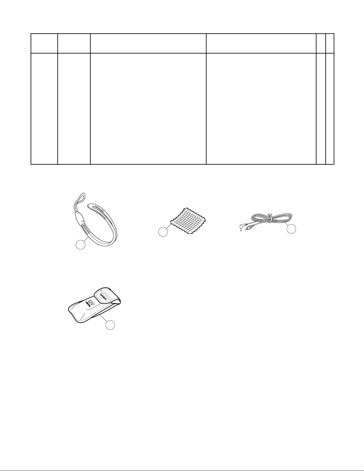
26. Accessories Wrist strap; soft case; video cable; cleaning cloth
— 1 —
Page 4
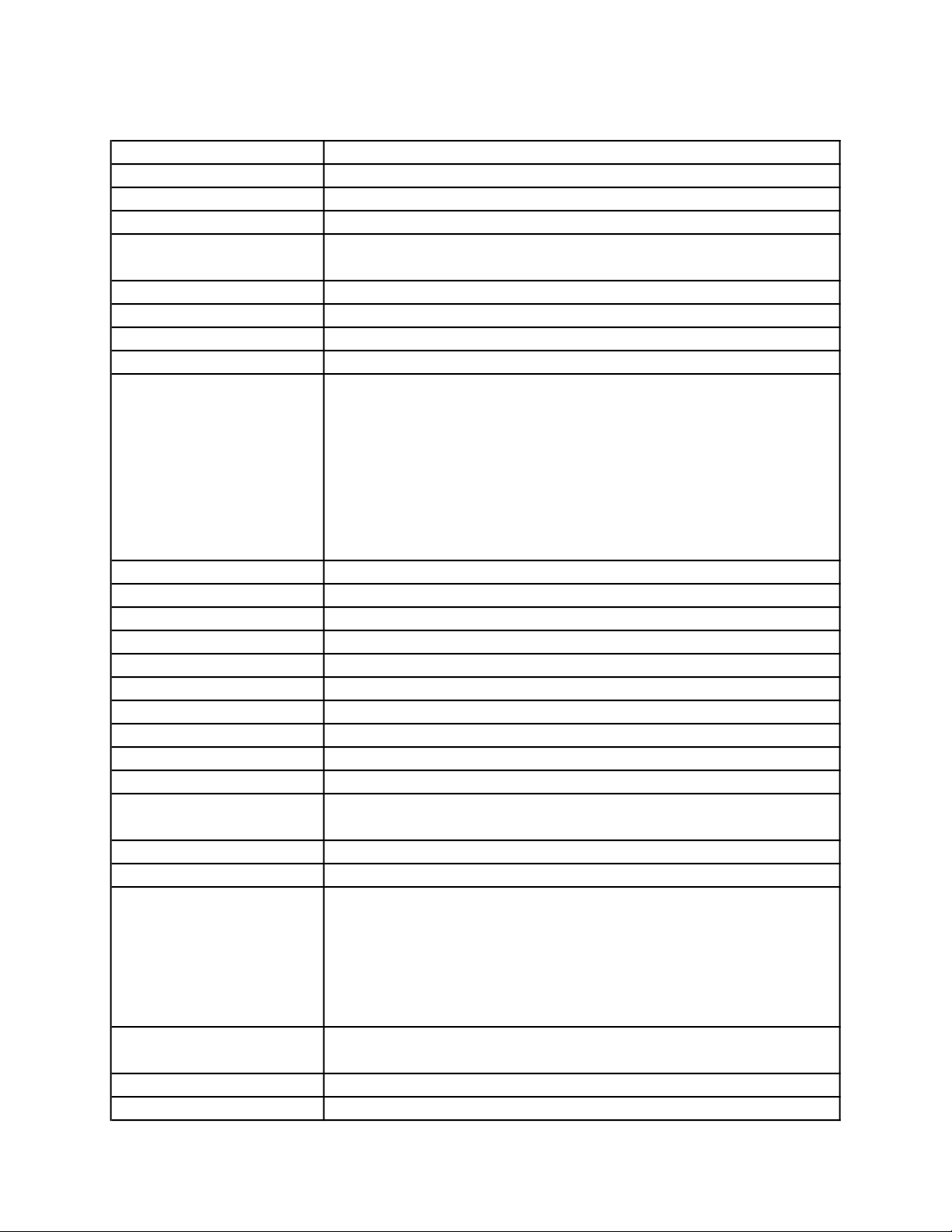
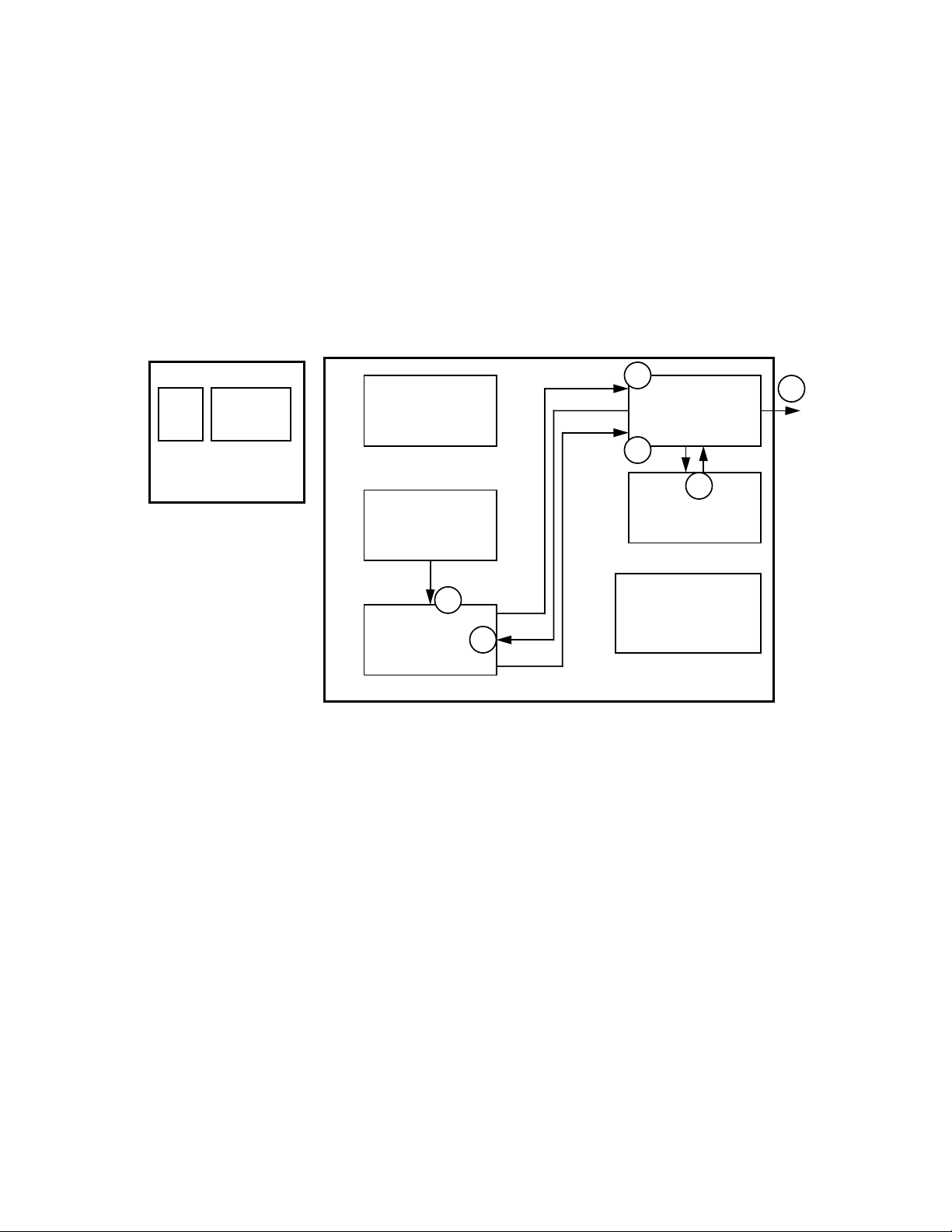
BLOCK DIAGRAM
Camera Unit Digital PCB
CCD
Lens
IC703
LC99092-Z03
8 bit to 16 bit
converter
Color processor
IC602
KM29V32000T
32 Mbit
Flash memory
IC601
HM51W4260
4 Mbit DRAM
A/D
converter
IC701
µPD482445LGW
4 Mbit VRAM
VRAM
controller
Data
compressor
expander
ROM
RAM
CPU
I/O
port
Direct
memory
access
controller
Bus
state
controller
Serial
communication
interface
IC702
µPD6461GS
On screen
display
Video
encoder
D/A
converter
IC700
HG51D291FE
Power
supply
Video out
Linear PCB
IC300
IR3Y21
Chroma circuit
IC400
MSM6770CGS
Display controller
Power
supply
Back
light
AC Adaptor
Battery
LCD
IC600
HD6437042Y03F
Key PCB
Digital I/O
— 2 —
Page 5
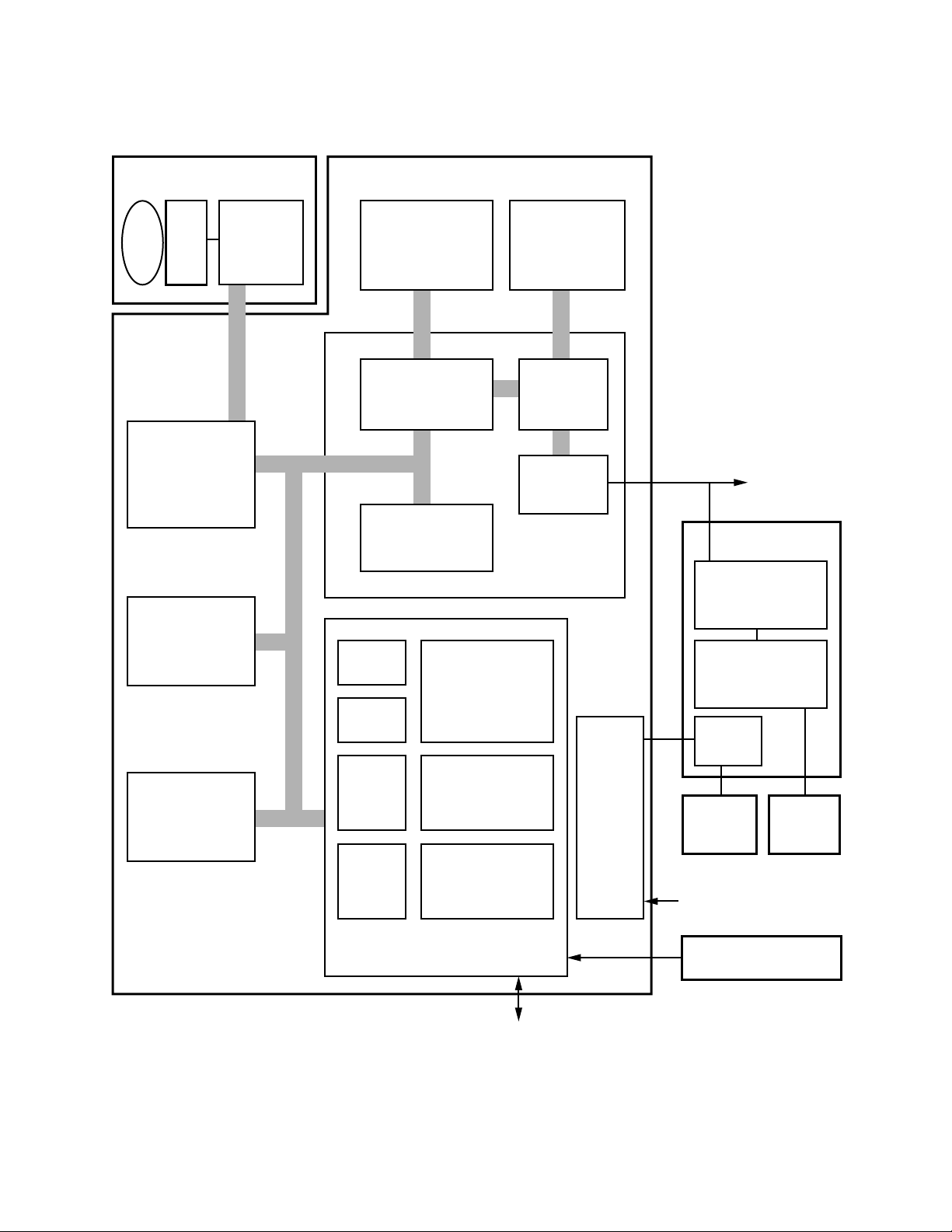
REC mode
1
CCD
Camera Unit
A/D
Converter
FLOW DIAGRAMS
2
IC703
LC99092-Z03
IC602
KM29V32000T
4
6
IC700
HG51D291FE
IC701
µPD482445LGW
7
8
3
IC601
HM51W4260
1 Exposure and Analog to Digital conversion by Camera unit
2 8 to 16 bits conversion by IC703
3 Storage for work
4 Color processing by IC703: Ye,Cy, Gr → Y, By, Ry
5 Storage for work
6, 7 Video encode by IC 700 and IC701: Y, By, Ry → Video
8 Video out
5
When pressing the shutter button
1
CCD
A/D
Converter
2
IC703
LC99092-Z03
4
IC600
HD6437042Y03F
Digital PCB
6
IC700
HG51D291FE
Camera Unit
IC602
KM29V32000T
8
IC601
HM51W4260
7
— 3 —
IC701
µPD482445LGW
3
IC600
HD6437042Y03F
5
Digital PCB
Page 6
1 Exposure and Analog to Digital conversion by Camera unit
2 8 to 16 bits conversion by IC703
3 Storage for work
4 Color processing by IC703: Ye, Cy, Gr → Y, By, Ry
5 Storage for work
6 Compression by IC700
7 Storage for work
8 Storage to Flash memory
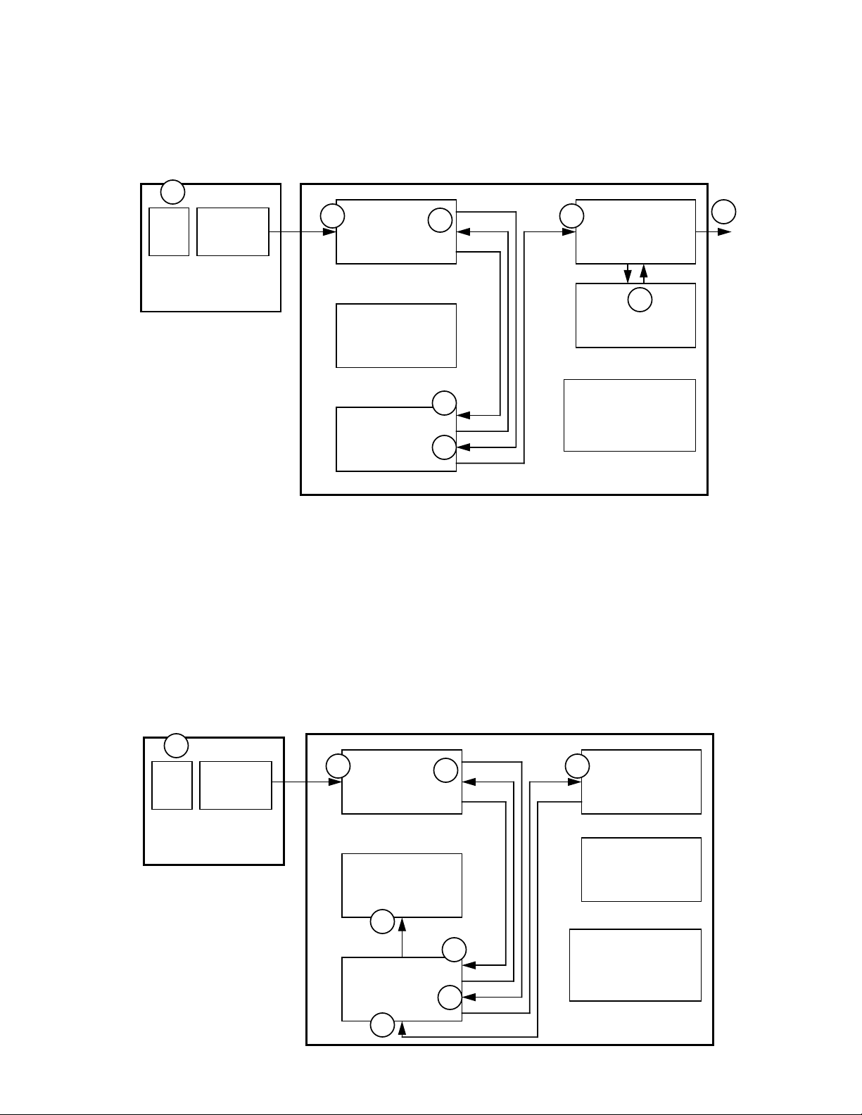
PLAY mode
CCD
A/D
Converter
IC703
LC99092-Z03
Camera Unit
IC602
KM29V32000T
1
IC601
HM51W4260
1 Reading from Flash memory and storage for work
2 Expansion by IC700
3 Storage for work
4, 5. Video encode by IC 700 and IC701: Y, By, Ry → Video
6 Video out
3
2
6
IC700
HG51D291FE
4
5
IC701
µPD482445LGW
IC600
HD6437042Y03F
Digital PCB
— 4 —
Page 7
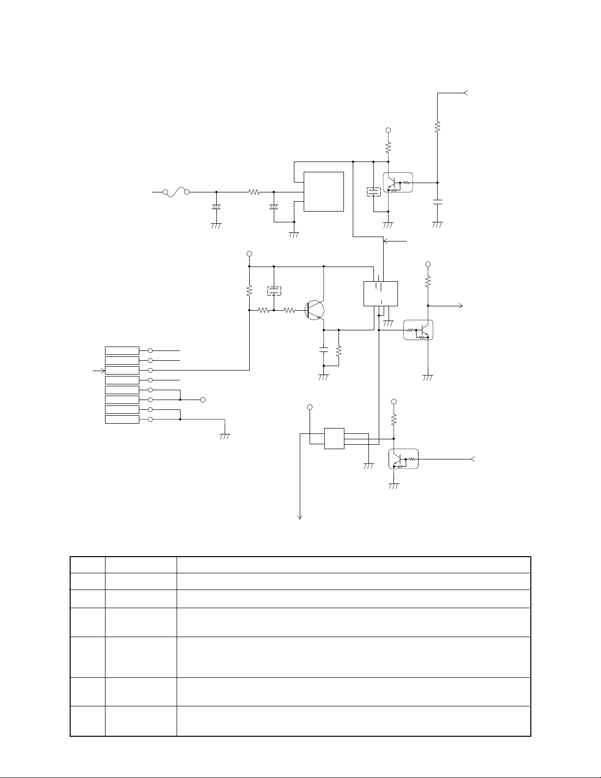
POWER SUPPLY CIRCUIT OPERATION
VCC1
R515
2 APO from Pin 42
of IC600
R517
1 PON from
Key PCB
CN601
KEY0
KEY2
PON
KEY1
VCC3-1
VCC3-1
GND
GND
FU500 R516
C548
1
2
3
4
5
6
7
VCC3-1
8
C531
VCC1
R511
++
R510
C520
R512
1
OUT
2
VDD
3
GND
3
C254
VCC1
IC507
1
2
4
OUT
5
VCC
NC
NC
Q503
R513
IC505
3
GND
2
INA
1
INB
Q514
2
5
1
C521
4
3
C523
6 Voltage detection signal
VCC3-1
876
5
Q
PR
CLR
VCC
CKDQ
123
GND
4
VCC1
2
1
3
Q513
R509
Q512
R514
2
1
3
3 POB to Pin102
of IC600
4 FACT from
Pin 36 of IC600
5 Power ON to Pin 3 of Q505
Signal
1
2
3
PON
APO
POB
Power on/off signal (pulse) from SW900 on Key PCB
Auto power off signal (pulse) from pin 42 of IC600
Power on/off recognition signal to pin 102 of IC600
Operation
ON: H (VCC3) OFF: L (GND)
4
FACT
Forced power on signal from pin 36 of IC600
Forced ON: H (VCC3) OFF: L (GND)
ex. While writing to flash memory
5
Power On
Power on/off signal to pin 3 of Q505
ON: H (VCC1) OFF: L (GND)
6
Voltage
detection
Normal: H
Low voltage: L
— 5 —
Page 8
IC
Operation
Time Chart
Power on
1. PON
IC505
IC506
IC507
NAND gate
Flip-flop
Voltage detector
1
4
H (VCC1)
L
1
2
CK
Q
Pin 2 (VDD)
> 3.2 V
< 3.2 V
5
PR
CLR
Power off
1. PON
7
6
Pin 1 (OUT)
H
L
H (VCC1)
L
2. APO
3. POB
4. FACT
5. Power On
6. Voltage
detection
L
H (VCC3)
L
L
H (VCC1)
L
H (VCC0)
2. APO
3. POB
4. FACT
5. Power On
6. Voltage
detection
L
H (VCC3)
L
L
H (VCC1)
L
H (VCC0)
L
— 6 —
Page 9

Power off by APO
Power off by low voltage detection
1. PON
2. APO
3. POB
4. FACT
5. Power On
6. Voltage
detection
H (VCC1)
H (VCC3)
L
H (VCC3)
L
L
H (VCC1)
L
H (VCC0)
1. PON
2. APO
3. POB
4. FACT
5. Power On
6. Voltage
detection
H (VCC1)
L
H (VCC3)
L
L
H (VCC1)
L
H (VCC0)
L
Forced power on by FACT
1. PON
2. APO
3. POB
4. FACT
5. Power On
6. Voltage
detection
H (VCC1)
L
L
H (VCC3)
L
H (VCC1)
L
H (VCC0)
— 7 —
Page 10

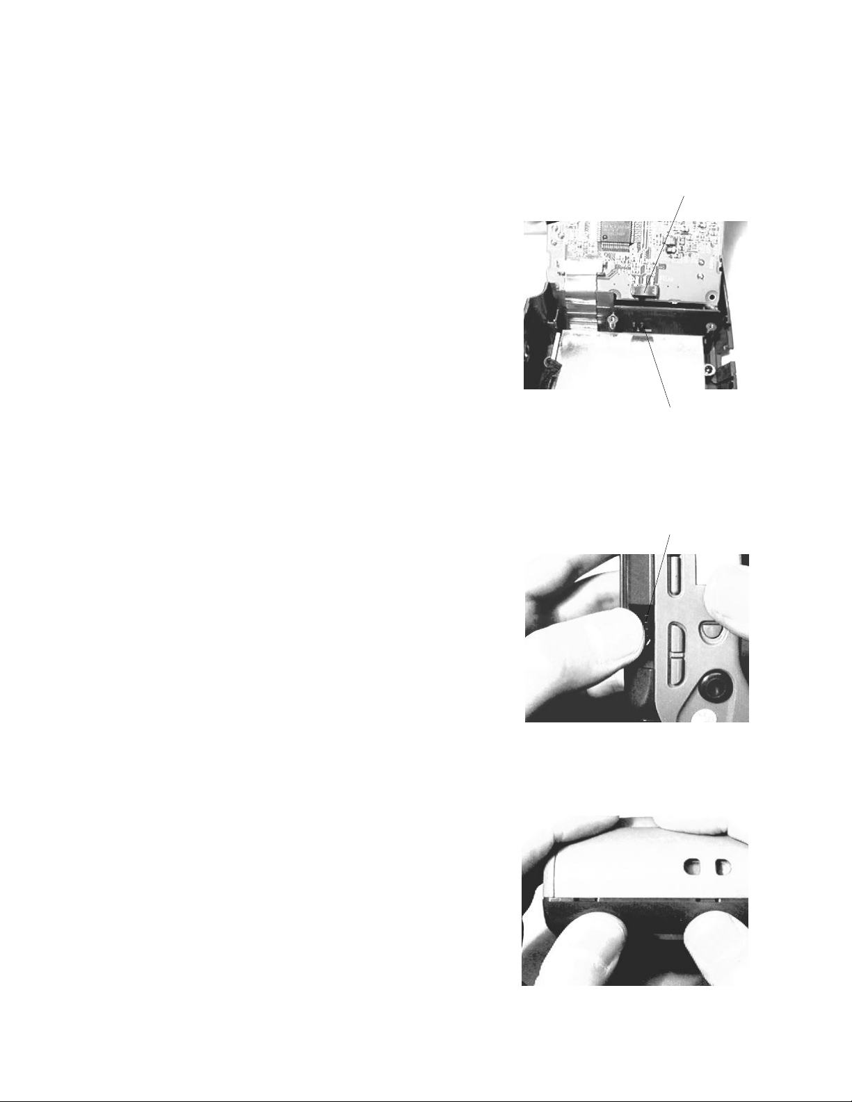
TROUBLESHOOTING
No Display
1. Check the fuse (FU500) on the digital PCB.
2. Check the fuse (FU100) on the linear PCB.
3. Check the jack (JK500) on the digital PCB.
4. Check the power switch (SW900) on the key PCB.
5. Check the flat cable between the digital and linear PCBs.
6. Check the back light.
7. Check the LCD.
No Display at Record Mode
1. Check the camera unit.
Defect of the Camera Unit
The camera unit must be replaced with whole unit when it is defective, because the precise adjustment is
required when the individual parts of the camera unit are replaced, and it can be done only at our factory.
(Except for replacing the outer case of the camera unit)
— 8 —
Page 11
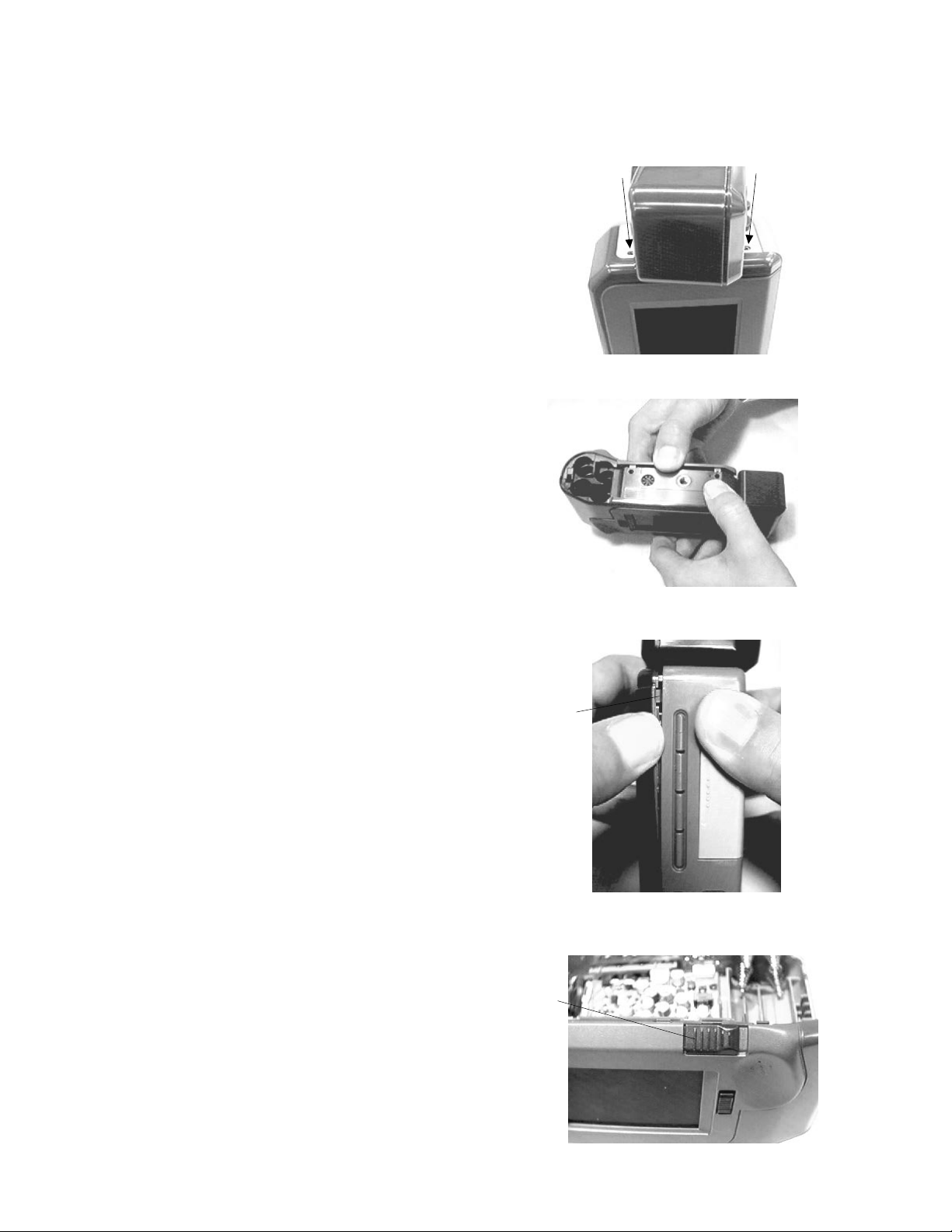
DISASSEMBLY
To disassemble the main unit
1. Rotate the camera unit then remove the two screws
on the side of the unit.
2. Remove the two screws on the bottom of the unit and
the battery cover. Then remove the upper case at
the bottom of the unit.
3. Then remove the upper case at the top of the unit.
4. Be careful not to lose the switch knob.
Hook
Switch knob
— 9 —
Page 12
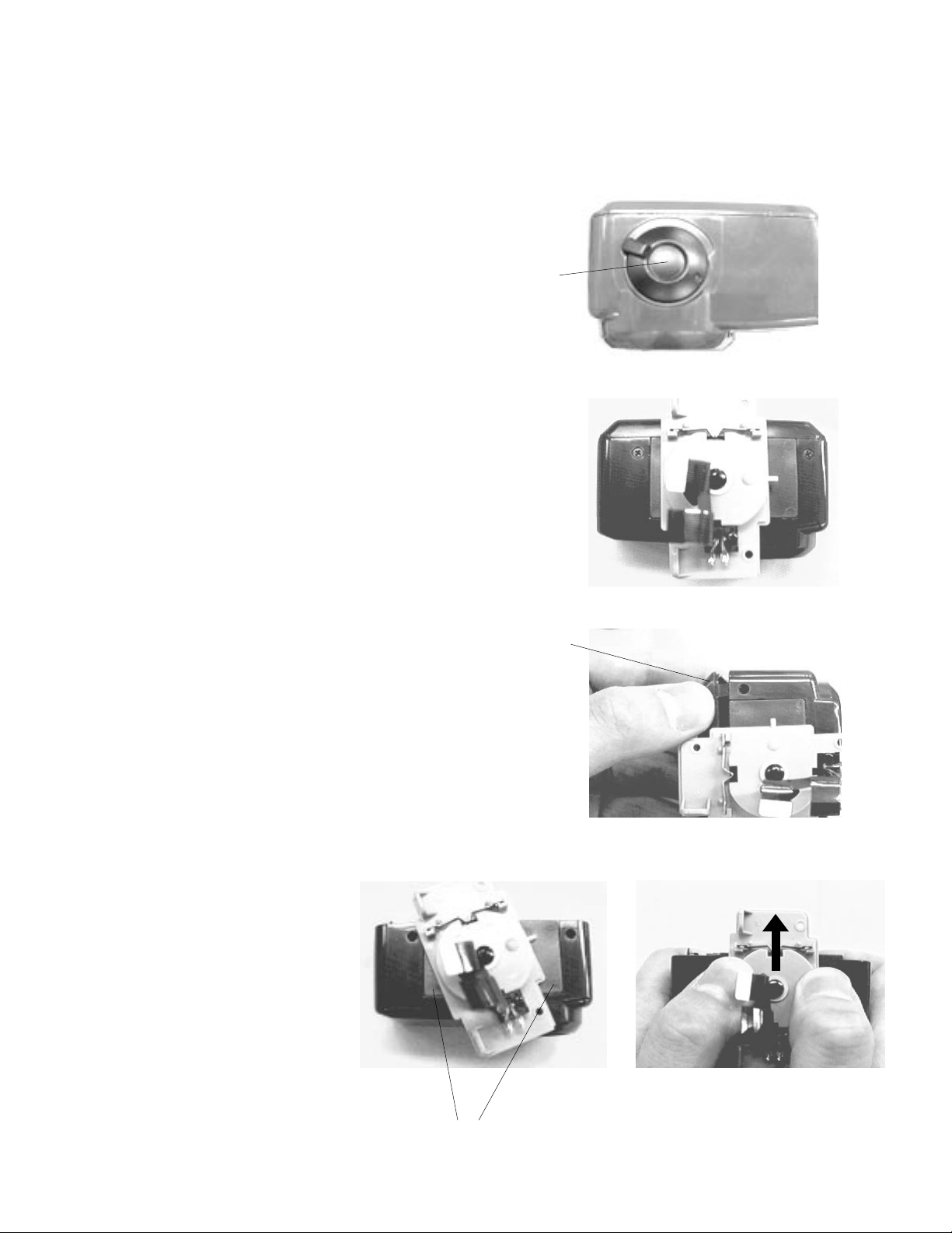
To disassemble the camera unit
Note: The camera unit must be replaced with whole unit when it is defective, because the precise adjustment
is required when the individual parts of the camera unit are replaced, and it can be done only at our
factory.
(Except for the replacing the outer case.)
1. Be sure to turn the lever to "TELE".
Lever
2. Remove the two screws.
3. Remove the cover of the camera unit at the
opposite side of the lever.
4. Unhook and remove the
lens and CCD unit from the
outer case as shown in the
picture.
Cover
Hook
— 10 —
Page 13
ASSEMBLY
To assemble the main unit
1. Be sure to align the slide switch on the linear PCB
with the switch knob.
2. Be sure to align the slide switch on the key PCB with
the switch knob.
Slide switch
Switch knob
Switch knob
3. Push hard the upper case with both hands.
— 11 —
Page 14

To assemble the main unit
1. Be sure to turn the lever to "TELE".
2. Be sure to align the lever of the outer case with the
knob of the lens.
Knob
3. Confirm if the lens is switched by the lever.
4. Be sure to align the switch knobs of the cover with
the switches.
Lever
Lens
Lever
Switch knob
— 12 —
Switch
Page 15
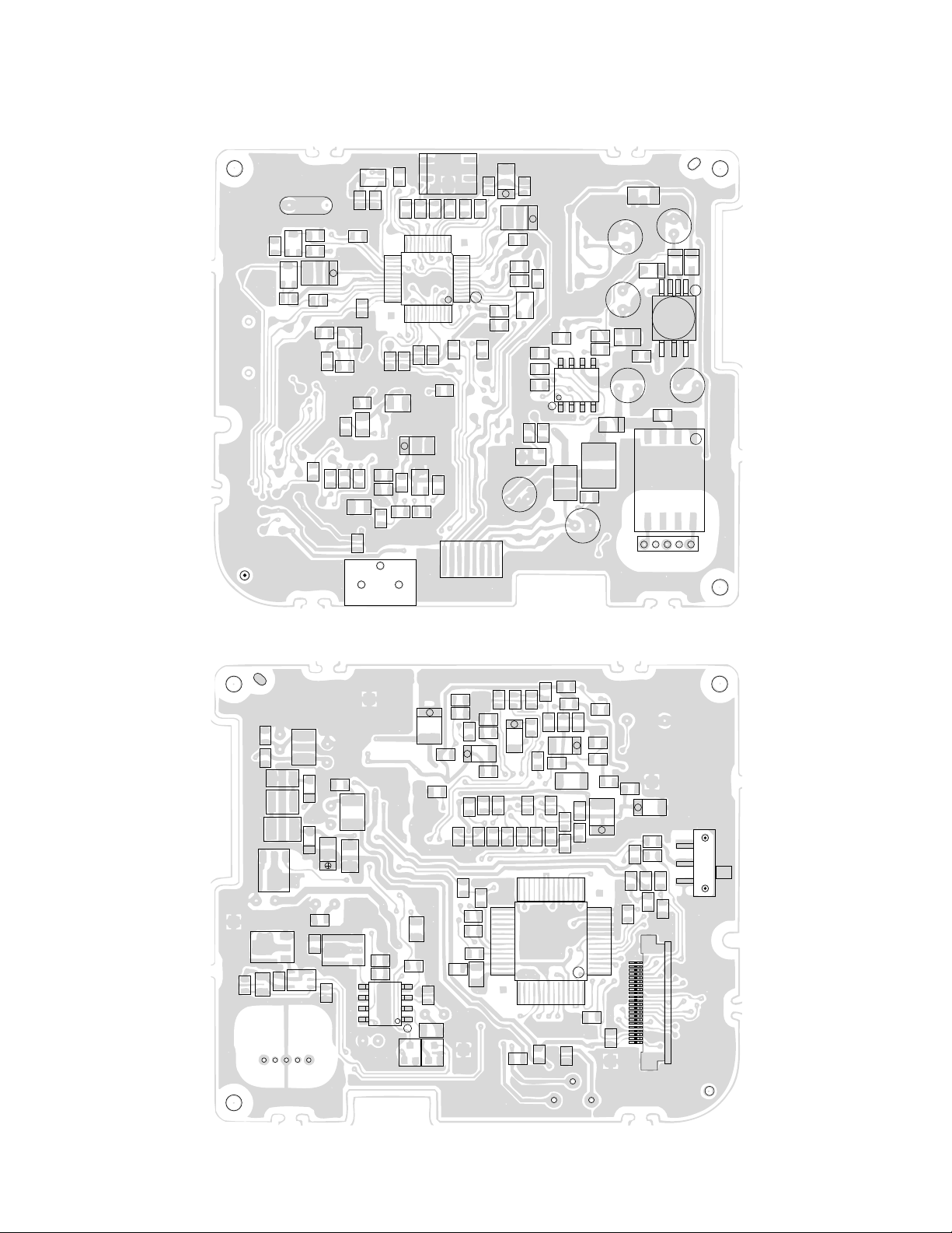
LINEAR
PRINTED CIRCUIT BOARDS
R317
R319
H300
VR303
VR302
C321
R316
C322
R318
R421
R401
+
R424
C408
Q401
R420
C318
R400
R414
C404
VR301
R430
R413
R426
C317
R313
C327
C414
R411
C405
VR304
C333
C409
+
R409 R408
R410
C316
R412
C338
R328
C401
C339
IC300
R331
VR400
L303
C340
R330
R403
C402
C311
C312
R320
CN100
C310
L300
1
C300
R301
R333
C309
R306
+
C307
+
R335
C303
C301
R300
VR300
R121
C111
R114
C110
1
R142
R141
VR101
+
C153
R110
R111
IC100
D105
L100
FU100
C141
+
C100
C120
C123
C125
C121
D103
+
D102
D101
+
1
+
VR100
++
C144
T100
C112
C101
C150
1
T150
CN150
R151
C122C124
C127
R120
L105
Q150
C152
Q100
IC150
C151
L102
D106 D104
C143
C142
C126
C129
Q101
R150
L103
C128
R113
C113
R115
IC101
1
Q102
+
C335
R304
C302
C145
C140
C146
Q103
Top View
R303
C308
R302
C306
R305
C305
+
C304
R340
R326
R327
C331
C332
C417
R404
R405
R406
R407
L400
C406
R308
C346
+
R325
C329
C337
C313
R332
R334
R307
R324
C336
C330
C413
R309
C320
C319
R312
R310
C314
C315
+
C334
R322R323
C347
C328
IC400
R321
R311
C324C348
1
C407
R336
R315
R314
+
L301
C323
C412
C325
+
R428
R402
C411
C326
R100
R427
C410
C416
CN400
SW100
R429
C415
Bottom View
— 13 —
Page 16
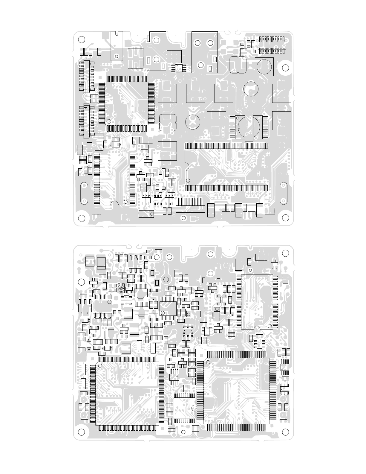
DIGITAL
C612
C613
C630
R633
R612
H701
R610
CN602CN603
C631
L732
R625
R626
C611
R603
C607
C527
C718
C629
EM2
R631
JK600
IC703
R607
D600
IC601
L643
L641
Q514
C625
R605
R606
R517
IC507
C531
Q508
R519
JK700
L740
L540
JK500
L502
IC605
C731 C730 C537 C541
L503
+
C544
C546 C542
C540
+
C551
Q610
IC701
Q611
R515
C521
R509
R629
Q512
C518
R516
C517
R630
CN600
C533
L513
L501
C601
C535
L631
C523
IC505 IC504
+
R521
+
T500
C534
R522
+
C548
C722
CN601
H700
C522
C506
C509
Q500
D503
C508
L506
R655
C704
R700
C705
L505
NR701 NR700
R701
FU500
Q510
R502
D500
D501
R504
C505
IC500
R503
C507
C519
C530
1
Top View
R523
IC502
C512
R505
IC503
L509
L507
R506
Q501
Q502
L510
NR703
Q609
C511
C536
D505
D504
L511
IC501
C545
R508
NR702
R507
C715
IC704
1
R518
C543
Q513
R608
C604
C605
C603
C714
C600
IC506
R640
R611
L734
Q701
R706 R707
C707
R513
R514
C524
Q503
IC702
R714
Q700
R705
1
C626
R713
+
F700
R703
L508
R702
L630
C525
R512
R511
R510
C520
R708
R709
R704
C720
C526
C606
Q702
R623
C609
C547
R711
R617
IC603
R530
1
R620
R621
R601
R501
R500
R602
VR500
R619
R600
Q505
D506
C501
1
Q507
C503
C504
Q506
Q504
R520
D502
IC700 IC600
Q613
R616
+
C721
Q612
D603
L600
D604
R622
R624
R614
R527
R528
L601
R615
C627
L602
D601
C624
L620
C602
C732
IC602
R641
IC604
D602
C623
1
R628
R627
C608
IC706
R632
IC705
C529
C528
R526
Bottom View
— 14 —
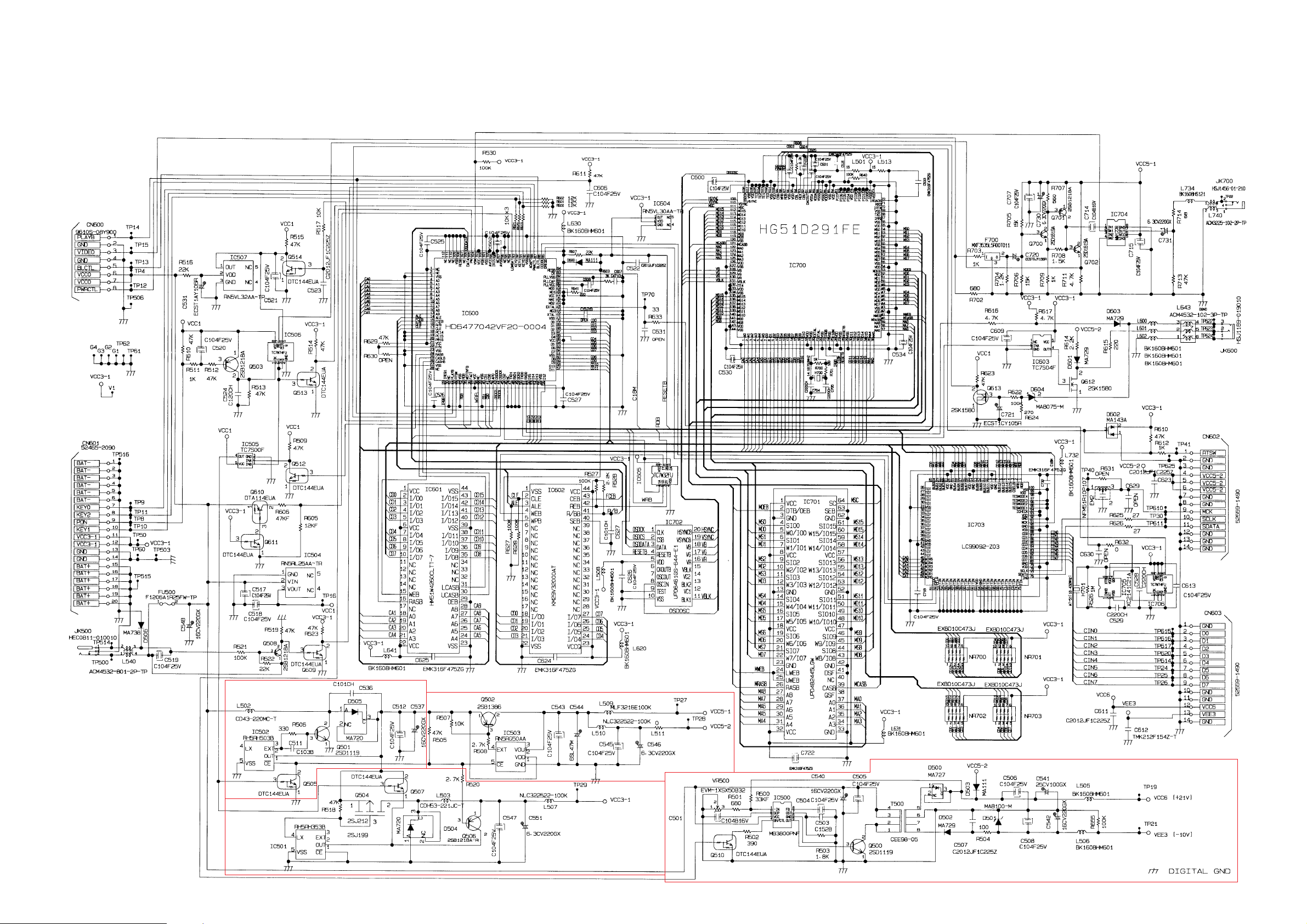
Page 17
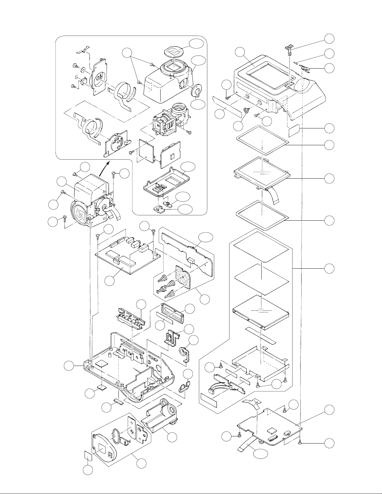
EXPLODED VIEW
30
27
30
31
28
27-4
27-5
27-6
27-1
27-2
27-3
2
1
28
5
6
28
4
3
7
8
9
31
19
18
29
26
22
29
24
10
25-1
11
25
23
21
20
29
16
29
14
17
13
15
29
12
29
29
12-1
— 15 —
Page 18
PARTS LIST
LINEAR PCB ASS'Y
Item Code No. Parts Name Specification Q R
Diodes
D101 7101 1194 Chip diode MA111-(TX) 1 C
D102 2390 1379 Schottoky diode MA729-(TX) 1 C
D103 2390 1379 Schottoky diode MA729-(TX) 1 C
D104 7101 1194 Chip diode MA111-(TX) 1 C
D105 2390 1379 Schottoky diode MA729-(TX) 1 C
D106 2360 2359 Chip zener diode MA8180-L(TX) 1 C
Fuse
FU100 3122 2772 Chip fuse ICP-S0.7TN 1 B
ICs
IC100 2114 3654 IC MB3800PNF-G-BND-EF 1 C
IC101 2114 3654 IC MB3800PNF-G-BND-EF 1 C
IC150 2105 3990 IC TC7S02F-TE85L 1 C
IC300 2114 5740 LSI IR3Y21 1 C
IC400 2015 0147 LSI MSM6770CGS-2K-6004 1 C
Transistors
Q100 2253 0308 Chip transistor 2SD1119-R(TX) 1 B
Q101 2253 0308 Chip transistor 2SD1119-R(TX) 1 B
Q102 7911 0126 Digital transistor DTC144EUAT106 1 B
Q150 2253 0700 Chip transistor 2SK1485-T1 1 B
Q401 2251 0189 Chip transistor 2SB1218A-R(TX) 1 B
Switch
SW100 3412 1106 Slide switch SSSS212-12 1 C
Converter and Transformaer
T100 3065 0693 DC-DC converter TTV6DD360M02 1 B
T150 3012 1477 Inverter transformer ETJ09K20AM 1 B
Variable resistor
VR304 2775 0644 Semi-fixed resistor H0614D-10KB 1 C
Notes: Q – Quantity used per unit
R – Rank
— 16 —
Page 19
DIGITAL PCB ASS'Y
Item Code No. Parts Name Specification Q R
Diodes
D500 2390 2268 Chip diode MA727-(TX) 1 C
D501 2360 1876 Chip zener diode MA8100-M(TX) 1 C
D502 2390 1379 Schottoky diode MA729-(TX) 1 C
D503 7101 1194 Chip diode MA111-(TX) 1 C
D504 2390 2261 Chip diode MA720-(TX) 1 C
D505 2390 2261 Chip diode MA720-(TX) 1 C
D506 2390 1421 Chip schottoky diode MA738-(TX) 1 C
D600 7101 1194 Chip diode MA111-(TX) 1 C
D601 2390 1379 Schottoky diode MA729-(TX) 1 C
D602 2390 1470 Chip diode MA143A-(TX) 1 C
D603 2390 1379 Schottoky diode MA729-(TX) 1 C
D604 2360 2982 Chip zener diode MA8075-M(TX) 1 C
Fuse
FU500 3632 0700 Chip fuse F1206A1R25FW-TP 1 A
ICs
IC500 2114 3654 IC MB3800PNF-G-BND-EF 1 C
IC501 2105 5985 IC RH5RH353B-T1 1 C
IC502 2105 3969 IC RH5RH503B-T1 1 C
IC503 2105 3689 MOS-IC RN5RG50AA-TR 1 C
IC504 2105 3976 IC RN5RL25AA-TR 1 C
IC505 2105 1407 CMOS-IC TC7S00F-TE85L 1 C
IC506 2105 5215 IC TC7W74FU(TE12L) 1 C
IC507 2105 3983 IC RN5VL32AA-TR 1 C
IC600 2012 5532 LSI HD6437042Y03F 1 C
IC601 2012 4424 LSI HM51W4260CLTT-7 1 C
IC602 2012 4340 LSI KM29V32000T 1 C
IC603 2105 1414 CMOS-IC TC7S04F-TE85L 1 C
IC604 2105 6006 IC RN5VL30AA-TR 1 C
IC605 2105 5719 IC TC7W32FU-TE12L 1 C
IC700 2012 4417 LSI HG51D291FE 1 C
IC701 2012 4354 LSI µPD482445LGW 1 C
IC702 2012 4711 LSI µPD6461GS-644-E1 1 C
IC703 2012 4431 LSI LC99092-Z03 1 C
IC704 2105 5992 IC MM1228XFR 1 C
IC705 2105 6288 IC XC2141C21A 1 C
IC706 2105 5215 IC TC7W74FU(TE12L) 1 C
Jacks
JK500 3501 8281 Jack HEC0811-010010 1 C
JK600 3501 6538 Jack HSJ1169-012010 1 C
JK700 3501 5439 Jack HSJ1456-01-210 1 C
Transistors
Q500 2253 0308 Chip transistor 2SD1119-R(TX) 1 B
Q501 2253 0308 Chip transistor 2SD1119-R(TX) 1 B
Q502 2251 0847 Chip transistor 2SB1386-T100R 1 B
Q503 2251 0189 Chip transistor 2SB1218A-R(TX) 1 B
Q504 2390 2863 Chip FET 2SJ212-T1 1 B
Q505 7911 0126 Digital transistor DTC144EUAT106 1 B
Q506 2251 0189 Chip transistor 2SB1218A-R(TX) 1 B
Q507 7911 0126 Digital transistor DTC144EUAT106 1 B
Q508 2251 0189 Chip transistor 2SB1218A-R(TX) 1 B
Q510 7911 0126 Digital transistor DTC144EUAT106 1 B
Q512 7911 0126 Digital transistor DTC144EUAT106 1 B
Notes: Q – Quantity used per unit
R – Rank
— 17 —
Page 20
Item Code No. Parts Name Specification Q R
Q513 7911 0126 Digital transistor DTC144EUAT106 1 B
Q514 7911 0126 Digital transistor DTC144EUAT106 1 B
Q609 7911 0126 Digital transistor DTC144EUAT106 1 B
Q610 2259 2205 Digital transistor DTA114EUAT106 1 B
Q611 7911 0126 Digital transistor DTC144EUAT106 1 B
Q612 2254 0448 Chip FET 2SK1580-T1 1 B
Q613 2254 0448 Chip FET 2SK1580-T1 1 B
Q700 2253 0133 Chip transistor 2SD1819A-R(TX) 1 B
Q701 2251 0189 Chip transistor 2SB1218A-R(TX) 1 B
Q702 2253 0133 Chip transistor 2SD1819A-R(TX) 1 B
DC-DC converter
T500 3701 0693 DC-DC converter CEE98-05 1 B
Notes: Q – Quantity used per unit
R – Rank
— 18 —
Page 21
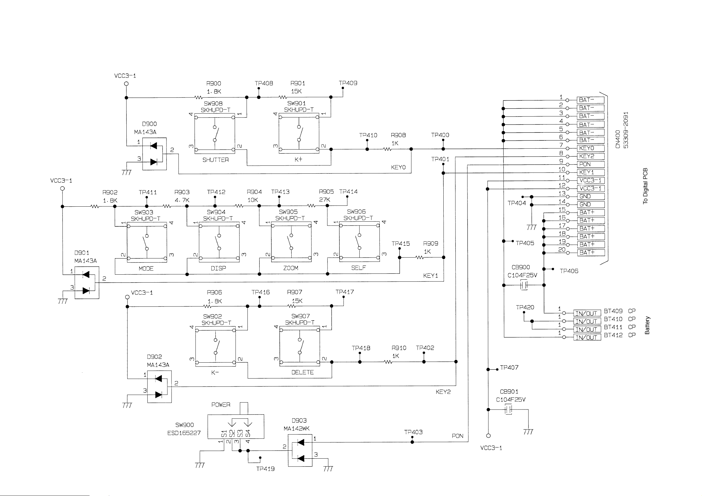
KEY PCB ASS'Y
Item Code No. Parts Name Specification Q R
Switches
SW900 3412 1421 Slide switch ESD165227 1 A
SW901 3412 0882 Switch SKHUPD-T 1 C
SW902 3412 0882 Switch SKHUPD-T 1 C
SW903 3412 0882 Switch SKHUPD-T 1 C
SW904 3412 0882 Switch SKHUPD-T 1 C
SW905 3412 0882 Switch SKHUPD-T 1 C
SW906 3412 0882 Switch SKHUPD-T 1 C
SW907 3412 0882 Switch SKHUPD-T 1 C
SW908 3412 0882 Switch SKHUPD-T 1 C
Notes: Q – Quantity used per unit
R – Rank
— 19 —
Page 22
MAIN COMPONENT
Item Code No. Parts Name Specification Q R
1 6611 6760 Upper case K727AAA C140275-2 1 X
2 6611 0680 R-P knob K724AAA C340701-1 1 X
3 6611 0440 Power switch knob K724AAA C340700-1 1 X
4 6611 7880 Power switch spring K727AAA R440130-1 1 X
5 6611 9230 Rating plate K727CCA C441158-7 1 X
6 6603 8924 C knob A-K310 K3741D-1 1 X
7 6611 0470 Battery label K724AAA C441180-1 1 X
8 6611 0690 Tape for LCD K724AAA C441068-1 1 X
9 2725 1329 LCD COD25T2018RB 1 B
10 6611 0700 Spacer for LCD K724AAA C441069-1 1 X
11 6611 0384 BL block C340812*1 1 B
12 6611 9420 Linear PCB ass'y R240051*2 1 B
12-1 6609 7340 Flat cable A-K720 K411997-1 1 B
13 6611 7848 Battery cover ass'y C340811*2 1 C
14 6611 5771 Battery cover label B-K725 K440205A-7 1 X
15 6611 0410 Battery holder K724AAA C340693-1 1 X
16 6611 6820 Blinder K727AAA C340695-2 1 X
17 6611 0460 Plate K724AAA C441170-1 1 X
18 6609 7440 Badge A-K720 K440063-1 1 X
19 6611 6752 Lower case K727AAA C140276B-2 1 X
20 6611 6730 Shutter button K727AAA C340698-2 1 X
21 6611 6740 DEL button K727AAA C340697-2 1 X
22 6611 6720 MENU button K727AAA C340699-2 1 X
23 6611 6810 Connector cover K727AAA C340696-2 1 X
24 6610 2540 Cover label B-K720 K440064-2 1 X
25 6611 7858 Key PCB ass'y C340813*2 1 C
25-1 3412 1421 Slide switch ESD165227 1 A
26 6611 9421 Digital PCB ass'y R240050*3 1 B
27 6611 7847 Camera unit C240573*2 1 B
27-1 6611 0510 Protector K724AAA C441074-1 1 X
27-2 6611 6830 Camera case A-K727AAA C240523-2 1 X
27-3 6611 0530 T-W knob K724AAA C340715-1 1 X
27-4 6611 6840 Camera case B-K727AAA C240524-2 1 X
27-5 6611 0550 Iris knob K724AAA C340713-1 1 X
27-6 6611 0540 Focus knob K724AAA C340714-1 1 X
28 5861 3434 Screw PT3 1.7X4.5 Ni 4 X
29 5860 1477 Screw BT3 1.7X3.5 Bk 12 X
30 5860 0301 Screw BT3 1.7X3.5 Ni 2 X
31 5112 0868 Screw BT3 1.7X5 Bk 2 X
Notes: Q – Quantity used per unit
R – Rank
— 20 —
Page 23
ACCESSORY
Item Code No. Parts Name Specification Q R
32 5861 2110 Wrist strap ST-K724 1 X
33 6611 1290 Cleaning cloth CC-K724 1 X
34 1014 8773 Video cable C-K723-FC 1 X
35 1014 9607 Soft case SC-727 1 X
Notes: Q – Quantity used per unit
R – Rank
32
35
33
34
— 21 —
Page 24
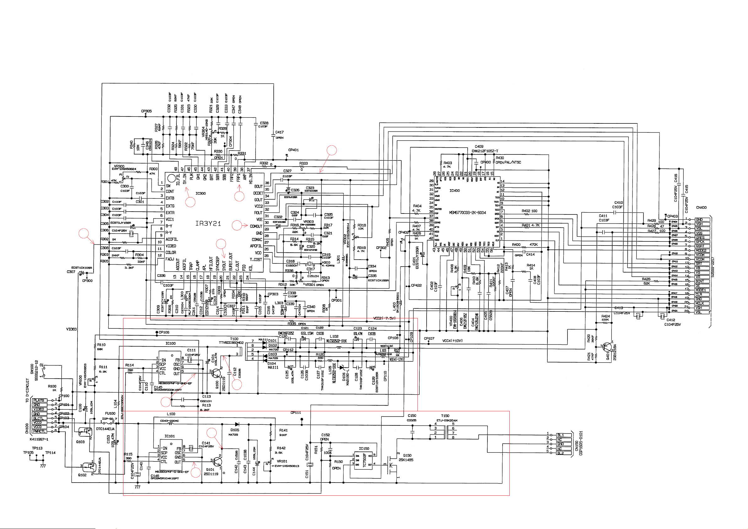
LINEAR
SCHEMATIC DIAGRAMS
9
REC/PLAY
7
8
Display Controller
Chroma IC
10
5
6
To LCD
To Digital PCB
2
1
4
Power Supply for LCD
To Back Light
3
Power Supply for Back Light
— 23 —
Page 25
DIGITAL
Data Expander
Data Compressor
Video Encoder
DRAM
CPU
Flash
Memory
On Screen Display
Digital I/O Video Out
8 to 16 bits Converter
Color processor
To Camera Unit
DC in To Key PCB To Linear PCB
5 V Booster Circuit
5 V Power Supply Circuit
VRAM
5 V
Power Supply Circuit for CCD
3.5 V
3.5 V Power Supply Circuit
— 24 —
Page 26
KEY
— 25 —
Page 27
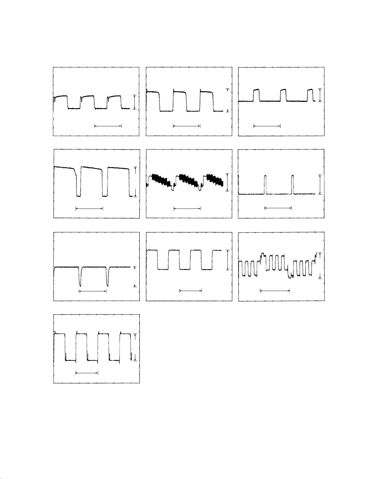
0.8 V
WAVEFORMS
0.8 V
10.0 V
4 µsec
1 IC100 pin 5
4 µsec 64 µsec
4 Q101 collector
64 µsec
7 IC300 pin 47
2 Q100 collector
7.0 V
5 IC300 pin 10
5.0 V
8 IC300 pin 39
4 µsec 4 µsec
3 IC101 pin 5
1.0 V
64 µsec
6 IC300 pin 20
5.0 V
125 µsec
9 IC300 pin 36
64 µsec
4.0 V
5.0 V
125 µsec
0 IC300 pin 30
6.0 V
— 27 —
Page 28

MA0200471A
 Loading...