

Page 1

SERVICE MANUAL
INDEX
(without price)
ELECTRONIC CASH REGISTER OPTION I/O BOARD
I/O-PB-12 (EX-I/O-PB-12)
NOV. , 1994
FOR MODEL: CE-4700
TK-1300
TK-2300
TK-2700
TK-5100
Page 2

Table of contents
1. In/On-line board
1-1.To mount the I/O PB-12 in the P/C unit.................................................................. 1
1-2.I/O PB-12 board cables connection........................................................................ 2
1-3.Interface.................................................................................................................. 3
2. In-line cable, Connector, and Terminator
2-1.In-line cable ............................................................................................................ 4
2-2.In-line connector ..................................................................................................... 5
2-3.In-line connector (ECR side) .................................................................................. 5
2-4.Terminator (This part is included with I/O-PB-12 product) ................................... 5
3. Connection
3-1.Cable connection diagram...................................................................................... 6
3-2.Connection on the PC side..................................................................................... 6
3-3.Connection on the end of in-lline cable .................................................................. 6
3-4.Connector between ECRs ...................................................................................... 6
4. Circuit explanations
4-1.Block diagram........................................................................................................ 7
4-2.ISA bus .................................................................................................................. 7
4-3.C-Inline ................................................................................................................... 8
4-3.Timing Chart......................................................................................................... 11
5. Diagnostic
5-1.Summary .............................................................................................................. 12
5-2.Files ...................................................................................................................... 12
5-3.Hardware .............................................................................................................. 12
5-4.Procedure ............................................................................................................. 12
5-5.Operation.............................................................................................................. 13
6. IC data ..................................................................................................
21
7. PCB layout ...........................................................................................
8. Circuit diagram....................................................................................
9. Parts list ...............................................................................................
22
23
29
Page 3
1. IN/ON LINE BOARD I/O PB-12
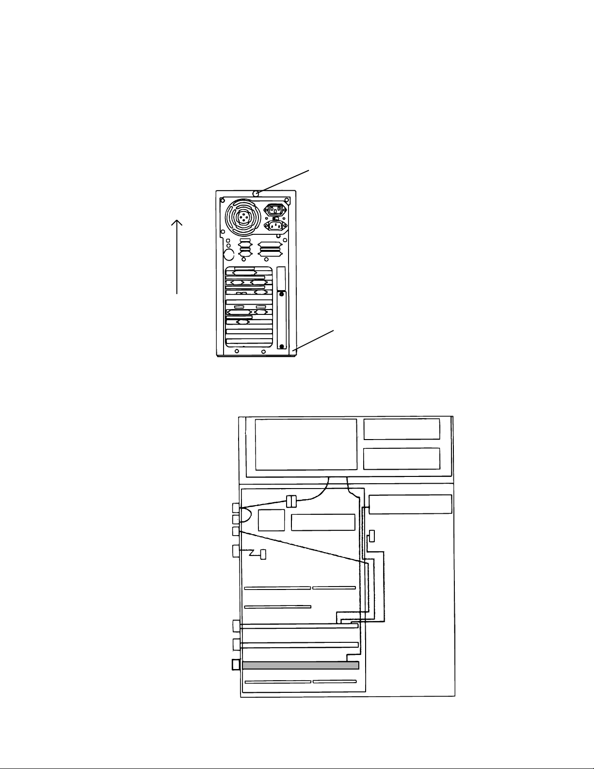
1-1. To mount the I/O pb-12 in the P/C unit
1) To open upper case of the P/C unit (In case using SA-3000 as a P/C unit), release the
one screw of the back side and lift the upper cas up from the CPU unit.
2) Lift up the upper case.
1) Release the screw.
NOTE: There are 6 hooks at the
bottom side of upper case. Please
be careful.
2) Mount the I/O PB-12 to the mother boards slot connector as shown in the following.
[Hardware Configuration]
BATTERY 1
UPS
BATTERY 2
Mother Board
CPU
RAM
R3 Printer cable
M/O Board
VGA BOARD
3.5 Inch FDD
HDD cable
I/O PB-12
— 1 —
Page 4
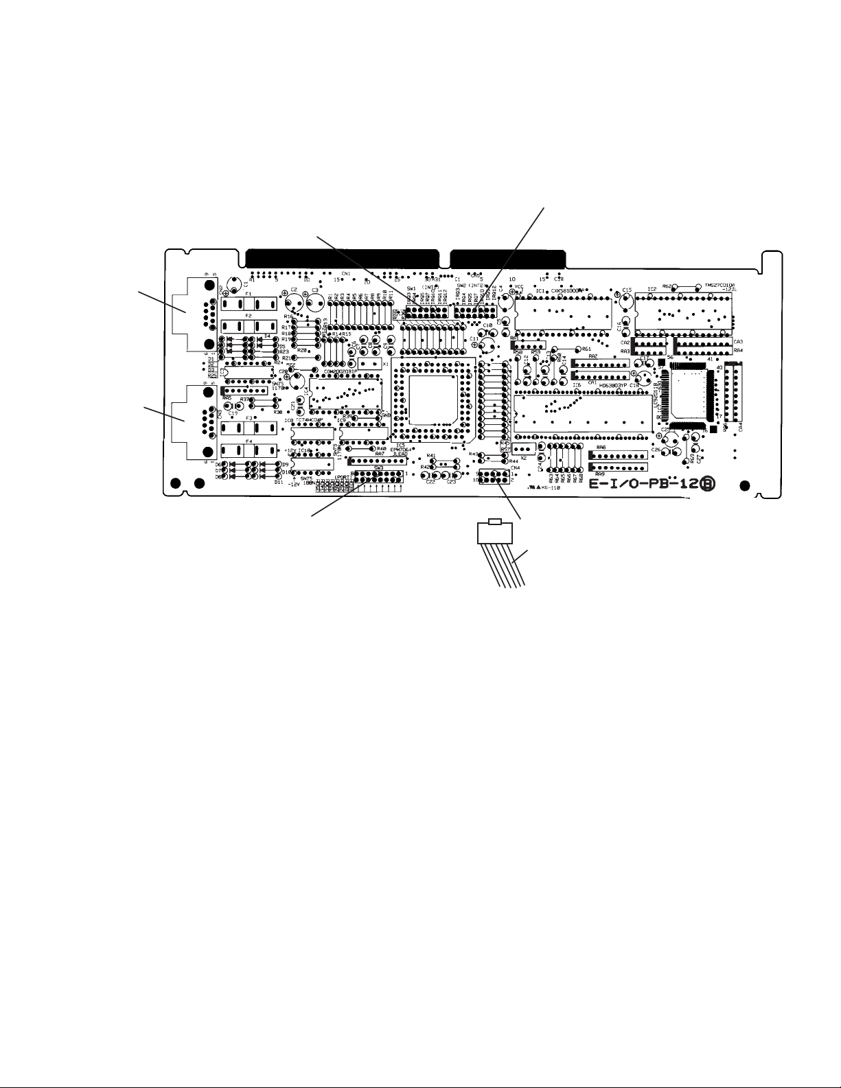
1-2. I/O PB-12 board cables connection
CN2
Inline
Connector
CN3
Kitchen
Printer
Connector
SW1
IRQ N o . selection
SW2
IRQ N o . selection
SW3
I/O Port address
selection
Red w ire
CN4
From Power supply (UPS)
1) Connect the following cable to the I/O-PB12.
CN2: Kitchen printer
CN3: In-line
CN4: Power cable from the UPS.
Ensure that the red dot line mark is No.1 pin.
2) The standard setting for SW1(INT1), SW2(INT2) and SW3(PORT) are as follows:
SW1: Standard setting is IRQ10.
SW2: Standard setting is IRQ11.
SW3: Standard setting is 1E0H.
— 2 —
Page 5
1-3. Interface
1-3-1. C In-line
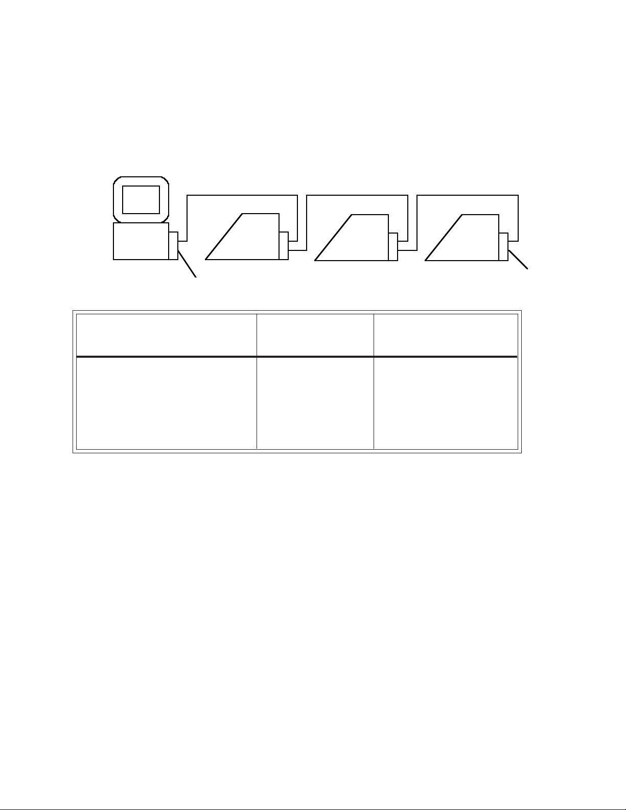
1) In-line connection diagram
The maximum in-line cable length and the maximum connection unit will be varied by the
in-line communication speed as shown below list.
[In-line cable wiring]
Total cable length is max. A m
ECRPC
Terminater(100 ohms)
ECR ECR
Terminater(100 ohms)
In-line Communication speed Maximum Maximum cable length
(Band rate) connection unit A (m)
1.25 M bps 8 86
625 K bps 12 200
312.5 K bps 20 430
156.25 K bps 32 890
2) Connection: Multi drop
3) Terminator: 100 Ω
4) We recommend that PC is a terminal set.
5) If PC is not the terminal set, FG(PC side) should not connect with cable ground.
Then to make 10 cm of cable which is non-terminal resist.
1-3-2. KP In-line
1) BPS speed: 1,200bps, 2,400bps, 4,800bps, 9,600bps, 19,200bps
2) Connection: T branch
3) Terminator: Open
4) We recommend that PC is a terminal set.
5) If PC is not the terminal set, FG(PC side) should not connect with cable ground.
Then to make a 10 cm of non-terminal resistor and to connect it in this case.
6) Dip switch
— 3 —
Page 6
[KP-200]
SW1: The blank means off.
Machine 1 2 3 4 BPS 5678
1
2 on 1200 Not used
3 on 2400
4onon
5 on 9600 on
6on on
7onon
8ononon
SW2 and SW3: All off
[KP-300]
SW1(Fixed): On: 4, 6 Off: 1,2,3,5,7,8
SW2: The blank means off.
Machine 1 2 3 4 BPS 5 6 7 8
600
4800 on on
1
2 on 1200 Not used
3 on 2400
4onon
5 on 9600 on
6on on
7onon
8ononon
600
4800 on on
2. IN-LINE CABLE, CONNECTOR, AND TERMINATOR
2-1. In-line cable
Code No. Parts name Specification
1904 4023 In-line cable IPEV-SLA 0.5x1
— 4 —
Page 7
[In-line cable specification]
1. Structure
2. Properties (20 °C)
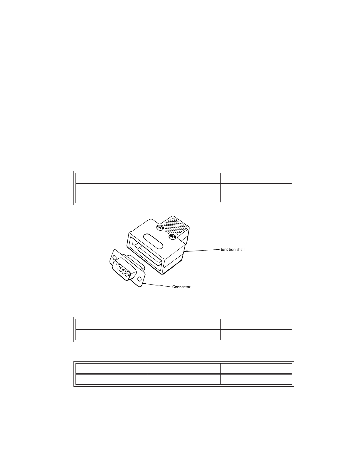
2-2. In-line connector
Code No. Parts name Specification
1904 4069 Connector DE-9PF-N10
1904 4070 Junction shell DE-C8-J9-F1
Conductor Material: Tin plated mild copper twist
Cross section area: 0.5 mm2
Construction: 20 pieces/0.18 mm
O.D. 0.95 mm
Insulation Material: polyethylene
Thickness: 0.3 mm
Sheath Material: PVC
Finished O.D 6.0 ~ 6.5 mm
Approx. weight 55 kg/km
Maximum conductor resistance 38.7 Ω/Km
Minimum insulation resistance 10 kMΩ•Km
Electric strength AC350 V/1 minute
Electrostatic Capacity (Standard) 75 nF/km
2-3. In-line connector (ECR side)
Code No. Parts name Specification
3500 5820 In-line connector kit XLP-KIT-1
2-4. Terminator (This part is included with I/O-PB-12 product)
Code No. Parts name Specification
2600 2516 Carbon film resistor R-25-100-J
— 5 —
Page 8
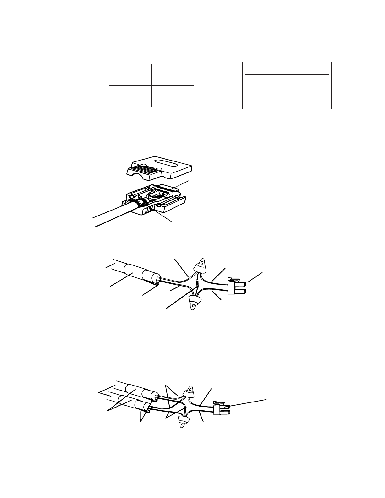
3. CONNECTION
Connect the in-line cable and in-line connector as shown as below:
3-1. Cable connection diagram
Signal Pin Signal Pin
SD 1 SD 1
RD 3 RD 2
FG FG plate FG Cut
( PC side ) ( ECR side )
3-2. Connection on the PC side
Termination 'R in series are connected at pins
1 and 4 of two connectors at both the ends of
the in-line cable.
Fold the shield and fasten by
wrapping copper tape.
3-3. Connection on the end of in-line cable
Red
In-line cable
Wrap bent shield wire
with Copper tape
Notes: 1. Use crimp tool for connecting terminal caps.
2. If crimp tool is not available, connect the wires with soled instead of
terminal cap. After the soldering, insulated the wire with vinyl tape.
Shield wire
Black
Terminator (100 ohms)
3-4. Connector between ECRs
Red
In-line cable
Red
Red
Black
In-line connector
In-line connector
Wrap bent shield wire
with Copper tape
Notes: 1. Use crimp tool for connecting terminal caps.
Shield wire
2. If crimp tool is not available, connect the wires with solder instead of
Black
terminal cap. After the soldering, insulated the wire with vinyl tape.
Black
— 6 —
Page 9
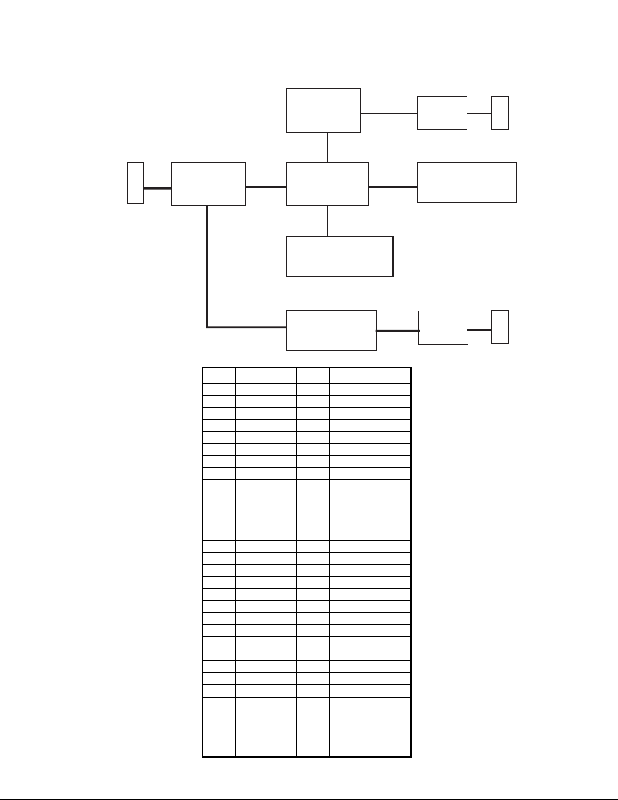
4. CIRCUIT EXPLANATIONS
4-1. Block diagram
ISA Bus
4-2. ISA bus
PLD
EPM7064
84pin J-Lead
Pin Signal Pin Signal
A01 NC B01 GND
A02 SD7 B02 RESETDRV
A03 SD6 B03 +5V
A04 SD5 B04 NC
A05 SD4 B05 NC
A06 SD3 B06 NC
A07 SD2 B07 -12V
A08 SD1 B08 NC
A09 SD0 B09 +12V
A10 IOCHRDY B10 GND
A11 AEN B11 NC
A12 NC B12 NC
A13 NC B13 IOW
A14 NC B14 IOR
A15 NC B15 NC
A16 NC B16 NC
A17 NC B17 NC
A18 NC B18 NC
A19 NC B19 NC
A20 NC B20 NC
A21 NC B21 IRQ7
A22 SA09 B22 NC
A23 SA08 B23 IRQ5
A24 SA07 B24 IRQ4
A25 SA06 B25 IRQ3
A26 SA05 B26 NC
A27 SA04 B27 NC
A28 SA03 B28 BALE
A29 SA02 B29 +5V
A30 SA01 B30 NC
A31 SA00 B31 GND
CPU
HD63B03YP
64pin DIP
GA
LC92011B-630
80pin FP
SRAM
CXK581000P-10L
32pin DIP
ARCNET
COM20020BP
24pin DIP
Driver
Receiver
EPROM
TM27C010A-12JL
32pin DIP
Driver
Receiver
KP In-line
C in-line
— 7 —
Page 10
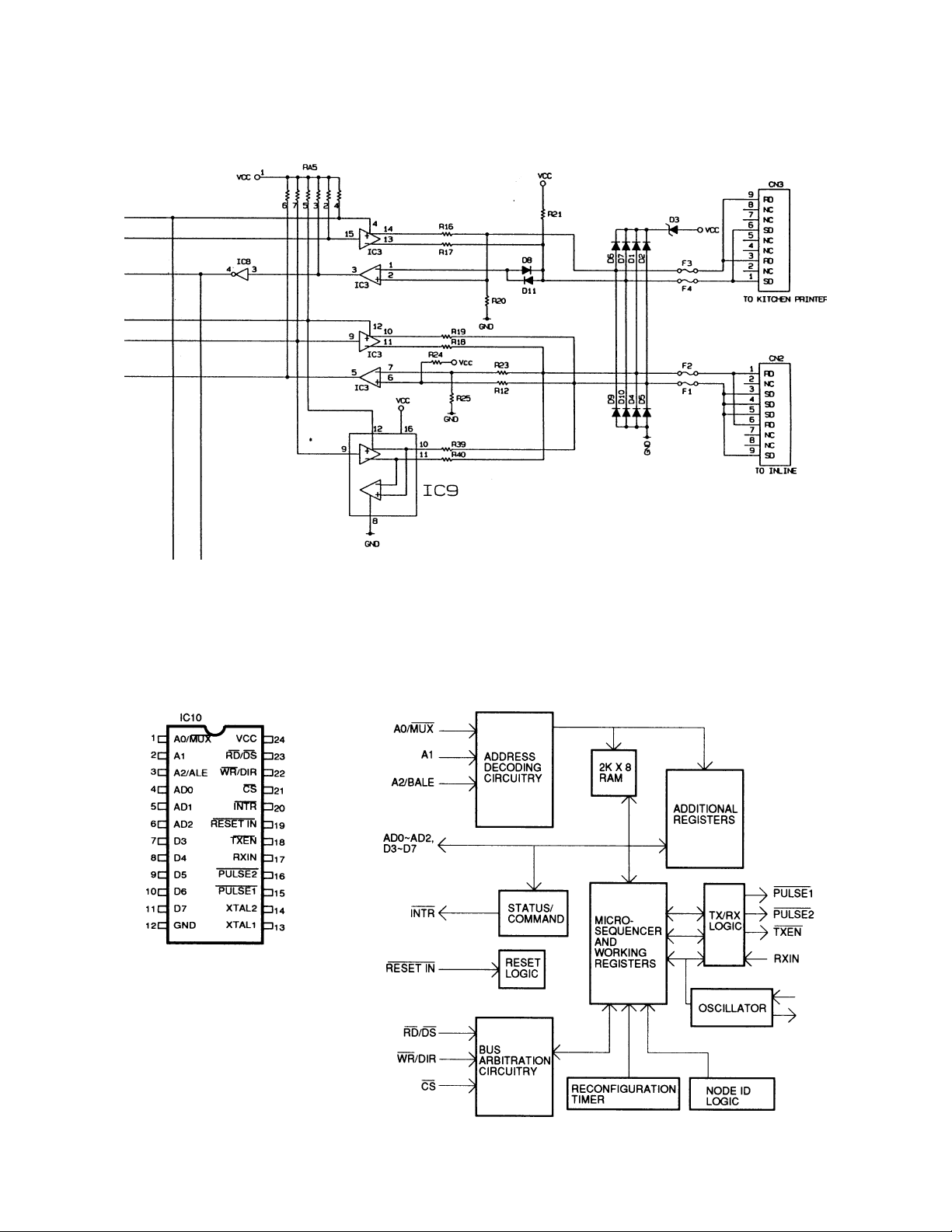
4-3. C-Inline
1. Circuit Diagram
[Pin Configuration] [Internal Block Diagram]
— 8 —
Page 11

2. COM20020B pin description
Pin No. Name In/Out Status Status Status Description
of OFF of ON of ON
No Token Token
1 A0/MUX In L L Pulse
2 A1 In L L L
3 A2/ALE In L L L
A0/MUX
A1
A2/ALE
4 AD0 In/Out L Pulse Pulse
5 AD1 In/Out L Pulse Pulse
6 AD2 In/Out L Pulse Pulse
7 D3 In/Out L Pulse Pulse
8 D4 In/Out L Pulse Pulse
9 D5 In/Out L Pulse Pulse
10 D6 In/Out L Pulse Pulse
11 D7 In/Out L Pulse Pulse
12 GND Power GND GND GND
13 XTAL1 In L Pulse Pulse
14 XTAL2 In L Pulse Pulse
15 PULSE1 Out L H Pulse
16 PULSE2 Out L L L
PULSE1
PULSE2
17 RXIN In L H Pulse
18 TXEN Out L L Pulse
19 RESET IN In L H H
TXEN
RESET IN
Input. On a non-multiplexed bus,
these signals are dirctly connectoed to
the low bits of the host address bus.
On a multiplexed address/data bus,
A0/MUX is tied low, A1 is left open,
and A2 is tied to the address latch
enable signal of the host. A1 is
connectoed to an internal pull-up
resistor.
Input/Output. On a non-multiplexed
bus, these signals are used as the
data lines for the device. On a
multiplexed address/data bus,
AD0~AD2 act as the address lines
(latched by ALE) and as the low data
lines for the device. D3~D7 are
always used for data only. These
signals are connected to internal pullup resistors.
Signal ground.
An external crystal shoul be connected
to these pins. If an external TTL clock
is used instead, it must be connected
to XTAL1 with a 390 ohms pull-up
resistor, and XTAL2 should be left
floating.
Output. In normal mode, these active
low signals carry the transmit data
information, encoded in pulse format,
from the COM20020 to the media
driver circuitry. When the device is in
backplane mode, the PULSE1 signal
driver is programmable (push/pull or
open-drain), while the PULSE2 signal
provides a clock with frequency of
crystal/4. PULSE1 is connected to a
week internal pull-up resistor in
backplane mode.
Receive input. This signal carries the
receive data information from the line
receiver circuitry to the COM20020.
Transmit Enable output. This signal
used in backplane mode to enable the
line drivers for transmission. The
polarity of the signal is programmable
by grounding the PULSE2 pin. This
option is valid only in backplane mode.
Input. This active low signal issued by
the microcontroller executes a
hardware reset. It is used to activate
the internal reset circuitry within the
COM20020.
— 9 —
Page 12

Pin No. Name In/Out Status Status Status Description
of OFF of ON of ON
No token Token
20 INTR Out L H Pulse
INTR
Interrupt output. This active low signal
is generated by the COM20020 when
an enabled interrupt condition occurs.
INTR returns to its inactive state when
the interrupt status condition or the
corresponding interrupt mask bit is
reset.
21 CS In L H Pulse
CS
Chip select input. This active low
signal issued by the microcontroller
selects the COM20020 for an access.
22 WR/DIR In L Pulse Pulse
WR/DIR
Input. On a 68XX-like bus, this signal
is issued by the microcontroller as the
Read/Write signal to determine the
direction of data transfer. In this case,
a logic "1" selects a read operation,
while a logic "0" selects a write
operation. In this case, data is
actually strobed by the DS signal. On
an 80XX-like bus, this active low
signal is isuued by the microcontroller
to indicate a write operation. in this
case, a logic "0" on this pin, when the
COM20020 is accessed, enables data
from the data bus to be written to the
device.
23 RD/DS In L L Pulse
RD/DS
Read/ Data strobe signal input. On a
68XX-like bus, this active low signal is
issued by the microcontroller as the
data strobe signal to strobe the data
onto the bus. On a 80XX-like bus, this
active low signal is issued by the
microcontroller to indicate a read
operation. In this case, a logic "0" on
this pin, when the COM20020 is
accessed, enables data from the
device to the data bus to be read by
the microcontroller.
24 VCC Power GND +5V +5V
Power supply +5V.
— 10 —
Page 13

4-4. Timing Chart
1. EP Rom read
2. S Ram write
— 11 —
Page 14

5. DIAGNOSTIC
5-1. Summary
5-2. Files
5-3. Hardware
1. In-line ( 1 to 1 : Connection type)
2. In-line ( 1 to Multiple : Connection-Less type )
3. Rom Check
4. Ram Write/Read
5. KP testing Print
6. The status for UPS
7. UPS DC cutting
1. C_SETUP.EXE
2. C_NETDRV.COM
3. C_DIAG.EXE
1. I/O-PB-12
2. PC(IBM-AT) and Display
3. ECR
Model: CE-4700,TK-1300,TK-2300,TK-2700,TK-5100
4. KP
Model: KP-200, KP-300
5. In-line cable
6. KP Cable
Note: Ensure that ID=1, speed= 4,800bps for KP.
5-4. Procedure
1. To connect In-line, KP and UPS under power off mode.
2. Load C_SETUP.EXE and press Enter.
3. Load C_NETDRV.COM and press Enter.
4. Load C_DIAG.EXE and press Enter.
— 12 —
Page 15

5-5. Operation
5-5-1. C_SETUP.EXE
Load C_SETUP.EXE and press Enter.
CASIO (R) SETUP Utility for I/O-PB-12, Version 0.02
Copyright(c) CASIO COMPUTER CO.,Ltd. All right reserved.
Which port Address ?
—> 1) 1E0
Choose 1 - 6 from above ( default = 1E0): __
Which hardware Interrupt Address For C_NET ?
—> 5) 10
Choose 1 - 6 from above (default = 10): __
2) 280
3) 290
4) 2A0
5) 320
6) 330
7) 340 Input the number and press Enter
8) 350
1) 3
2) 4
3) 5
4) 7
6) 11 Input the number and press Enter
7) 12
Which Hardware Interrupt Address For KP ?
1) 3
2) 4
3) 5
4) 7
5) 10
—> 6) 11 Input the number and press Enter
7) 12
Choose 1 - 6 from above (default = 11): __
— 13 —
Page 16

My Node Number (default = 254): __ Input 1 ~ 254 and press Enter
BPS(default = 0) / 0(156.25K), 1(312.5K), 2(625K), 3(1.25M) : __ Input 0 ~ 3 and press Enter
Do you use UPS (SA3000 only) (Yes /No) ? (default = Yes): __ Input the Yes or No and press Enter
Write the file (Yes/No) ? : __ Input the Yes or No and press Enter
5-5-2. C_NETDRV.COM
Store in the resident area: Load C_NETDRV and press Enter.
Restore from the resident area: Load C_NETDRV -R and press Enter.
The message will be displayed as follows:
1) C_NETDRV.COM is stored in the memory.
CASIO Network Driver / Version 0.02
Cop[y right (c) CASIO COMPUTER CO.,Ltd. All right reserved.
Hardware configuration: IO: 1E0 / IRQ: 10 / Service Vector: 87
Installed.
2) C_NETDRV.COM is already stored in the memory.
CASIO Network Driver / Version 0.02
Cop[y right (c) CASIO COMPUTER CO.,Ltd. All right reserved.
C_NET DRIVER already exist in memory.
3) C_NETDRV.COM is restored from the memory.
CASIO Network Driver / Version 0.02
Cop[y right (c) CASIO COMPUTER CO.,Ltd. All right reserved.
C_NET DRIVER Removed.
— 14 —
Page 17

5-5-3. C_SETUP.EXE
Load C_DIAG and press Enter.
POS_check Exist();
= 0001 (If the driver is not exist, No more message and to be error end.)
POS = read ID(); = ca02 (If the ID is wrong, No more message and to be error end.)
POS_read Version(); = 0002 (Version for driver)
board_chk(); = 0001 (If the I/O-PB board is not exist, No more message and error end.)
*******************************************************************************************************
* DIAG For I/O-PB-12 Ver 0.03 *
*******************************************************************************************************
* NETWORK TEST ( C_NET CHIP ) * CPU TEST *
*******************************************************************************************************
1: NET START 11: CPU Software RESET & Set DIAG Mode
2: NET END 12: ROM Sum Check
3: SEND/RECV MODE (Connection) 13: RAM Check ( Write & Read )
4: RECS/SEND MODE (Connection) 14: RAM Check ( Read only )
5: SEND MODE (Connection Less) 15: Ram Check ( Write & Read/ Repeat )
6: RECV MODE (Connection Less) 16: Ram Check ( Read only / Repeat )
7: SEND MODE Not allowed 17: KP_PRINT_OUT
8: RECV MODE Not allowed 18: KP_PRINT_OUT ( Repeat )
19: ROM & RAM & KP
*******************************************************************************************************
21: UPS STATUS 98: DRV INF
22: UPS DC CUT 99: END
*******************************************************************************************************
ENTER DIAG Number : =>
1) Input the number and press Enter.
2) Thereafter testing program, The display will be going back to menu screen as above.
3) All testing program can quit by <ESC> key, then going back to menu screen.
Note: 1. Test program No. 7 and 8 are not allowed. (Only software testing)
2. In case of that test programming No. 3, 4, and 6 are not working as long as
No. 5 is working, The IRQ setting of C_NET may clash with the other software.
[Each test command programming]
1. NET START
To initialize the Network and Network controller.
You have to install this program first, before using program 3. ~ 6. or after using
the program No. 2.
u_ioctrl ( start ) ret = 0000
— 15 —
Page 18

2. NET END
To quit Network and Network controller and stop the token.
u_ioctrl ( end ) ret = 0000
3. SEND/RECV MODE (Connection)
To repeat In-line communication. ( 1 to 1)
In case of communication error, Going to retry 10 times at every 0.5 second.
Ensure that install the program No.1 before using this operation.
Send to ( Target ECR Number ):__ Input the ECR ID and press Enter.
n_mk_socket ret = 0000
n_bind ret = 0000 ECR side: After setting ID and BPS speed.
n_open ret = 0300 Then input 840<#2>.
HIT RETURN KEY TO GO NEXT Press Enter.
n_write ( Loop = 0001 )
Counting up the number of packet.
Blinking n_write and n_read. Press Esc.
n_close ret = 0000
n_del_sckt ret = 0000
4. RECV/SEND MODE (Connection)
To repeat In-line communication. ( 1 to 1)
In case of communication error, Going to retry 10 times at every 0.5 second.
Ensure that install the program No.1 before using this operation.
Recv from ? ( Target ECR Number ):__ Input the ECR ID and press Enter.
n_mk_socket ret = 0000
n_bind ret = 0000 ECR side: After setting ID and
n_open ret = 0300 BPS speed. Then input 830<#2>.
HIT RETURN KEY TO GO NEXT Press Enter.
n_read ( Loop = 0001 )
Counting up the number of packet.
Blinking n_write and n_read. Press Esc.
n_close ret = 0000
n_del_sckt ret = 0000
— 16 —
Page 19

5. SEND MODE (Connection-Less)
The communication for 1 to Multiple.
In case of communication error, does not retry or resend any more.
Ensure that install the program No.1 before using this operation.
Send to ( Target ECR Number ):__ Input the ECR ID and press Enter.
n_mk_socket ret = 0000
n_bind ret = 0000 ECR side: After setting ID and
n_open ret = 0300 BPS speed. Then input 860 <#2>.
HIT RETURN KEY TO GO NEXT Press Enter.
n_write ( Loop = 0001 )
Counting up the number of packet.
n_close ret = 0000 Press Esc.
n_del_sckt ret = 0000
6. RECV MODE (Connection-Less)
The communication for 1 to multiple.
In case of communication error, does not retry or resend any more.
Ensure that install the program No.1 before using this operation.
Recv From ( Source ECR Number ):__ Input the ECR ID and press Enter.
n_mk_socket ret = 0000
n_bind ret = 0000 ECR side: After setting ID and
n_open ret = 0300 BPS speed. Then input 850<#2>.
HIT RETURN KEY TO GO NEXT Press Enter.
n_write ( Loop = 0001 )
Counting up the number of packet.
n_close ret = 0000 Press Esc.
n_del_sckt ret = 0000
7. 8. Not allowed
— 17 —
Page 20

11. CPU Software RESET & Set DIAG Mode
To initialize the CPU.
You have to install this program first, before using program 12. ~ 19. or after CPU
rocking out for noise examination.
Send CPU RESET Command
Send OK
Wait Response From CPU !
Result = OK !!
Please Wait !! ( For CPU Initialize)
Send DIAG_SET_MODE Command
Send OK
Wait Response From CPU !
Result = OK !!
HIT RETURN KEY TO GO NEXT Press Enter
12. ROM Sum Check
Verify for Rom sum check.
Ensure that install the program No.11 before using this operation.
Get Rom Version
Send OK
Wait Response From CPU !
Result = OK !!
Rom_Version = 2772
Send ROM_CHK Command
Send OK
Wait Response From CPU !
Result = OK !!
HIT RETURN KEY TO GO NEXT Press Enter
13. RAM Check (Write & Read )
Ram read and write check.
Ensure that install the program No.11 before using this operation.
Send Ram Check ( W / R ) Command
Send OK
Wait Response From CPU !
Result = OK !!
HIT RETURN KEY TO GO NEXT Press Enter
— 18 —
Page 21

14. RAM Check ( Read only )
Ram read check.
Ensure that install the program No.11 and 13 before using this operation.
Send Ram Check ( Read ) Command
Send OK
Wait Response From KP !
Result = OK !!
HIT RETURN KEY TO GO NEXT Press Enter
15. RAM Check ( Write & Read / Repeat )
To repeat program No. 13 RAM Check (Write & Read )
Ensure that install the program No.11 before using this operation.
Send Ram Check ( W / R ) Command
Send OK
Wait Response From CPU !
Result = OK !!
( Hit Esc Key stop )
HIT RETURN KEY TO GO NEXT Press Enter
16. RAM Check ( Read only / Repeat )
To repeat program No. 14. RAM Check ( Read only )
Ensure that install the program No.11 and 13 before using this operation.
Send Ram Check ( Read ) Command
Send OK
Wait Response From KP !
Result = OK !!
( Hit Esc Key stop )
HIT RETURN KEY TO GO NEXT Press Enter
— 19 —
Page 22

5-5-4. Diagnostic program error code
Code Details
8080 A PW-On Error of C-NET chip.
8081 A receiving permission of C-NET could not be reset.
8082 A ID of C-NET is not set up.
8083 No token on the In-line circuit.
8084 A sending data is too much.
8085 A sending is not exist. / No token on the In-line circuit.
8086 A NCB (Network Control Block) is not enough.
8091 A network could not be open.
8092 A network could not be close.
8095 A network could not be synchronizing
8099 A sending retry is over.
809B A sending / receiving block is counter mis-match.
809C A sending application is not exist or stop.
809D A receiving memories are empty.
809E A sending queued time is out. (WAK retry over.)
809F No sending response.
80C6 A sending time out for a waiting
— 20 —
Page 23

6. IC Data
TC74HC04P TC74HC04P SN751178N
— 21 —
Page 24

7. PCB LAYOUT
TMS27C010A
-12JL
R62
IC2
C15
CA3
RA4
41
56
57
C17
C18
40
17
RA6
CA4
16
1
C25
C27
R69
80
IC7
C26
LC92011B
-630
RA8
HD63B03YP
CA1
IC6
RA2
C16
CA2
RA3
R61
C14
R60
C13
C12
R59 R58
RA1
C5
CXK581000AP
C18
15
IC1
10
VCC
C4
IRQ4
IRQ5
IRQ7
IRQ10
IRQ11
IRQ12
CN5
5C1
SW2( INT2 )
IRQ3
C10
C11
IRQ3
IRQ4
IRQ5
IRQ7
IRQ10
IRQ11
IRQ12
SW1
( INT1 )
30 A31 25
20
~
R26
R36
R1
R2
R3
R4
R5
R6
R7
R8
R9
R10
R11
CN1
15
C9
C8
C7
C6
R14R15
C3
C2
10
R16
R20
R13
R12
R17
R18
R19
5
D4
D5
R23
R21
R22
R24
A1
F1
F2
C1
CN2
9
5
1
6
5
9
IC3
D1D2D3
R25
RA5
C19
R37
F3
CN3
C20
SN75
1178N
IC4
C21
R38
IC8
TC7
4HC04P
COM20020BIP
R39
IC9
X1
GND
350H
340H
330H
320H
2A0H
290H
280H
1E0H
IC5
EPM7064
JLEAD
R40
RA7
SW3
SN75
1178N
18
(PORT)
F4
+12V
IC10
D9
D10
-12V
D11
SN75
188N
R41
R42
C22C23
R43
9
10
~
R45
R57
D6D7D8
1
6
R63
R64
R65
R66
R67
R68
X2
R44
CN4
1
2
C24
KS-110
RA9
R1
R2
R3
R4
R5
R6
R7
R8
R9
R10
R11
IRQ3
IRQ4
IRQ5
IRQ7
IRQ3
IRQ10
CN2
C4
9
5
C1
F1
A1
5
C2
10
C3
15
CN1
20
SW1
( INT1 )
30 A31 25
SW2
CN5
5C1
( INT2 )
10
VCC
IC1
15
C18
CXK581000AP
C15
IC2
R62
-12JL
TMS27C010A
B1
CN1
B31
CN5
D5 D3
D16
D18
6
1
D8D7D6
D11
D9
D10
-12V
188N
(PORT)
8
1
9
1
C24
RA9
SW3
R42
CN4
C27
R69
SN75
1178N
R44
X2
RA7
IC5
R41
R43
IC10
SN75
350H
340H
330H
320H
2A0H
290H
280H
1E0H
C22
C23
10
2
R63
R64
KS-110
R65
R66
R67
R68
F4
+12V
R40
JLEAD
EPM7064
~
R57
R45
RA8
C26
CN3
IC8
IC9
80
C25
1
16
RA6
CA4
C19
F3
R38
C21
TC7
4HC04P
R39
GND
LC92011B
IC7
17
RA5
R37
SN75
IC4
-630
9
5
D3D2D1
R25
IC3
1178N
C20
COM20020BIP
C14
IC6
CA1
HD63B03YP
C18
57
40
C12
R24
R22
X1
R60
C13
R21
C17
56
41
6
1
RA2
R23
R20
C6
C7
C8
C9
R58
R59
R61
RA3
RA4
F2
D4
D5
R19
R18
R17
R16
R12
R13
R14
R15
R26
~
R36
IRQ10
IRQ11
IRQ12
IRQ4
IRQ5
C11
CA2
CA3
RA1
IRQ7
IRQ11
C10
IRQ12
C5
C16
Top View
— 22 —
Bottom View
Page 25

8. CIRCUIT DIAGRAM
BCDEFGHI JKA
1
1
CN1
A1
IE0H
280H
290H
320H
330H
340H
350H
A2
A3
A4
A5
A6
A7
A8
A9
A10
A11
A12
A13
A14
A15
A16
A17
A18
A19
A20
A21
A22
A23
A24
A25
A26
A27
A28
A29
A30
A31
TO MOTHER BOARD
SW3
16
1
15
2
14
3
13
4
12
5
11
6
10
7
9
8
VCC
SD7
SD6
SD5
2
3
4
5
6
7
TO E-I/O-PB-12(2/6)
SD4
SD3
SD2
SD1
SD0
AEN
SA09
SA08
SA07
SA06
SA05
SA04
SA03
SA02
SA01
SA00
I/O 1
I/O 2
I/O 3
I/O 4
I/O 5
I/O 6
I/O 7
I/O 8
(PORT)
2A0H
23456789
RA7
B1
B2
B3
B4
B5
B6
B7
B8
B9
B10
B11
B12
B13
B14
B15
B16
B17
B18
B19
B20
B21
B22
B23
B24
B25
B26
B27
B28
B29
B30
B31
GND
GND
VCC
C1
GND
C2
–12V
+12V
C3
(INT1)
IRQ10
IRQ11
IRQ12
D1D2D3D4D5D6D7D8D9
CN5 TO MOTHER BOARD
IRQ3
IRQ4
IRQ5
IRQ7
(INT2)
IRQ10
IRQ11
IRQ12
IRQ3
IRQ4
IRQ5
IRQ7
SW1
1
14
2
13
3
12
4
11
5
10
6
7
9
8
SW2
1
2
3
4
5
6
7
D10
14
13
12
11
10
9
8
D11
D12
D13
D14
D15
D16
D17
D18
RST
IOW
IOR
IRQ1
IRQ2
2
TO E-I/O-PB-12(2/6)
3
4
5
6
7
1
8
BCDEFGHI JKA
GND
— 23 —
C1C2C3C4C5C6C7C8C9
Board No.
E-I/O-PB-12 (1/6)
C10
C11
C12
C13
C14
C15
C16
C17
C18
8
E312044
Page 26

BCDEFGHI JKA
TO E-I/O-PB-12 (3/6)(4/6)(5/6)
1
A0A1A2A3RD
WR
2
VCC
3
D0
D1
D2
D3
D4
4
D5
D6
TO E-I/O-PB-12 (3/6) (4/6) (5/6)
D7
RAMCE 1
RAMCE0
(4/6)
IOCS
CPURST
(3/7)(4/7)
2345
5
RAMCE
(5/7)
INT 1
(3/6)
INT 2
6
1
RA1
R57
R56
R51
R47
R55
R54
R53
R52
R50
R49
R48
12
13
14
15
16
17
18
19
20
21
22
23
24
25
26
27
28
29
30
31
32
C10
111098765432184838281807978777675
A0A1A2
A3
RD
WR
OE2
OE1
VCC
AEN
VCC
OE2OUT
SA03
SA04
GND
POWER
VCC
SA05
BATT
SA06
GND
D0
VCC
D1
D2
D3
D4
D5
GND
D6
D7
RAMCE1
RAMCE0
IOCS
VCC
CPURST
INT1
INT2
RAMCE
GND
IRQ1
IRQ2
BALE
333435363738394041424344454647484950515253
TO E-I/O-PB-12 (1/6)
GND
DCCUT
OE1OUT
SA07
GND
SA08
I/O8
I/O8
SA09
VCC
IOW
I/O7
I/O7
IOR
I/O6
I/O6
RST
I/O5
IC5
I/O5
I/O4
I/03
GND
I/O2
I/O1
CSART
ARCINT
ARCRST
VCC
SA0
SA1
SA2
SD0
SD1
SD2
GND
SD3
SD4
SD5
SD6
SD7
VCC
I/O4
I/O3
I/O2
I/O1
POWER
BATT
DCCUT
1
2
VCC
R22 R14
74
73
72
71
70
69
68
67
66
65
64
63
62
61
60
59
58
57
56
55
54
GND
C20
IC4
1
A0
2
A1
3
A2
4
D0
5
D1
6
D2
7
D3
8
D4
9
D5
10
D6
11
12
TXOUT
D7
GND
C21
VCC
INTR
RST
TXEN
RXIN
RD
WR
CS
24
23
22
21
20
19
18
17
16
15
14
X2
13
X1
VCC
R13
R15
TXEN
RXIN
TXOUT
X1
C8 C7 C6
3
TO E-I/O-PB-12 (6/6)
4
5
6
C9
C11
GND VCC
7
8
R46
IRQ1
R45
IRQ2
R36
AEN
R35
SA03
R34
SA04
R33
R32
SA05
R31
SA06
R30
R29
SA07
SA08
TO E-I/O-PB-12 (1/6)
R28
SA09
IOW
R27
IOR
R26
RST
R1R2R3R4R5R6R7R8R9
SD7
SD6
SD5
SD4
SD3
SD2
SD1
SD0
SA2
R10
SA1
R11
SA0
Board No.
E-I/O-PB-12 (2/6)
7
8
E211761
BCDEFGHI JKA
— 24 —
Page 27

BCDEFGHI JKA
1
VCC
1
RA2
2
CA1
3
4
5
6
7
8
9
1
GND
D7
D7
( 2/6 ) ( 4/6 ) ( 5/6 )
E ( 4/6 )
RD
WR
2
C12
C13
C14
VCC
3
4
R58
R59
R60
64636261605958575655545352515049484746454443424140393837363534
E
RD
LIR
WR
R/W
IC6
GND
D0D1D2D3D4D5D6
D0D1D2D3D4D5D6
BA
2
3
4
5
6
7
8
9
D0D1D2D3D4D5D6
A0A1A2A3A4A5A6A7A8
GND
A0A1A2A3A4A5A6
A7
VSS1
A8
A9
A9
A10
A10
D7
A11
A12
A11
A13
A12
A13
A14
A14
A15
VCC
A15
33
VCC
D0–D7
A0–A15
TO E–I/O-PB-12 (2/6) (4/6) (5/6)
C18 C17
GND
1
2
3
4
VSS
XTAL
EXTAL
MP0
MP1
RES
STBY
NMI
P20
P21
P22
P23
P24
P25
P26
P27
P50
P51
P52
P53
P54
P55
P56
P57
P60
P61
P62
P63
P64
P65
P66
123456789
GND
5
2
X2
1
3
C24 R63
GND
1011121314151617181920212223242526272829303132
R64
VCC
2 3 4 5 6 7 8 9 2 3 4 5 6 7 8 9
R65
R66
RA8
R67 R68
1
VCC
RA9
6
7
P67
1
VCC
INT2
INT1
CPURST ( 2/6 ) ( 4/6 )
TXD
RXD
RTS
( 2/6 )( 6/6 )
5
6
7
8
SCICLK ( 4/6 )
8
Board No.
E-I/O-PB-12 (3/6)
E211762
BCDEFGHI JKA
— 25 —
Page 28

BCDEFGHI JKA
1
IOCS ( 2/6 )
ROMCE ( 5/6 )
RAMCE0 ( 2/6 )
RAMCE1 ( 2/6 )
2
3
4
1
2
3
4
5
6
( 3/6 ) SCICLK
( 2/6 ) ( 3/6 ) ( 5/6 ) WR
( 2/6 ) ( 3/6 ) ( 5/6 ) RD
( 3/6 ) E
( 2/6 ) ( 3/6 ) CPURST
7
8
R69
Vcc
GND
C27
C25
C26
GND
1
2
3
4
5
6
7
8
9
10
11
12
13
14
15
16
8079787776757473727170696867666564636261605958
VSS
IOCS
SLIPSFM
SLIPSCK
KDCSTM
KDCSCK
KDCSFM
DOTSCK
VSS
DOTSFM
VDD
CLKOUT
WRITE
READ
E
RESET
BTSTS
CISTS
MODCOM
CLKCOM
RXD
RXK
RXOUTD0D1
1718192021222324252627282930313233343536373839
D0D1D2D3D4D5D6
CS2E
OPTCN
SWCOM
VLDSTS
VSSD2D3D4D5D6D7
PNESTS
VSS
SWI7
SWI6
PCSCK
PCSFM
D7
PCSTM
SWI5
VSSA0A1A2A3A4A5A6A7A8A9
A0A1A2A3A4A5A6A7A8A9A10
SWI4
SWI3
SWI2
SWI1
SWI0
ICCS
ICSEL
57
IC7
ROMCE
RAMCE2
RAMCE1
RAMCE0
RA18
VSS
RA17
RA16
RA15
RA14
VDD
RA13
A15
A14
A13
A12
A11
A10
40
GND
VCC
1
RA6
9
A0
8
A15
A14
A13
A12
A11
A1
A2
A3
A4
A5
A6
A7
A8
A9
A10
A11
A12
A13
A14
A15
7
6
5
4
3
2
9
8
7
6
5
4
3
2
RA4
56
55
54
53
52
51
50
49
48
47
46
45
44
43
42
41
RA16
RA15
RA14
RA13
9
8
7
6
5
4
3
2
1
GND
VCC
1
9
8
7
6
5
4
3
2
1
GND
RA13–RA16 ( 5/6 )
CA4
CA3
A0–A15
D0–D7
( 2/6 )
( 3/6 )
( 5/6 )
5
6
7
8
Board No.
E-I/O-PB-12 (4/6)
E211763
BCDEFGHI JKA
— 26 —
Page 29

BCDEFGHI JKA
1
WR
RO
2
D0-D7
A0-A15
RA13-RA16
(2/6)
(3/6)
(4/6)
(2/6)
(3/6)
(4/6)
(4/6)
3
4
1
2
3
4
GND
5
1
2
3
A12
4
A7
5
A6
6
D0
D1
D2
7
GND
A5
A4
A3
A2
A1
A0
6
7
8
9
10
11
12
13
14
15
16
C4
C5
IC1 IC2
NC
A16
A14
A12
A7
A6
A5
A4
A3
A2
A1
A0
I/O0
I/O1
I/O2
VSS
VCC
A15
CE2
WE
A13
A8
A9
A11
OE
A10
CE
I/O7
I/O6
I/O5
I/O4
I/O3
32
31
30
29
28
27
26
25
24
23
22
21
20
19
18
17
D7
D6
D5
D4
D3
Vcc
A8
A9
A11
A10
RA14
RA16
RA15
RA13
R61
A12
A7
A6
A5
A4
A3
A2
A1
A0
D0
D1
D2
GND
10
11
12
13
14
15
16
RA15
RA16
VCC
PGM
NC
A14
A13
A8
A9
A11
OE
A10
CE
I/O7
I/O6
I/O5
I/O4
I/O3
C16
C15
32
31
30
29
28
27
26
25
24
23
22
21
20
19
18
17
GND
1
VPP
2
A16
3
A15
4
A12
5
A7
6
A6
7
A5
8
A4
9
A3
A2
A1
A0
I/O0
I/O1
I/O2
VSS
D7
D6
D5
D4
D3
Vcc
A13
A8
A9
A11
A10
R62
RA14
RA13
RA14
RA15
RA16
5
VCC
1
RA3
5
4
3
2
GND
5
4
3
2
1
CA2
ROMCE
6
(4/6)
7
RAMCE
(2/6)
8
8
Board No.
E-I/O-PB-12 (5/6)
E211764
BCDEFGHI JKA
— 27 —
Page 30

BCDEFGHI JKA
1
RTS
TXD
2
TO E-I/O-PB-12 (3/6)TO E-I/O-PB-12 (2/6)
3
RXD
TXEN
TXOUT
RXIN
R37
C19
GND
IC8
R38
21
Vcc
VCC
IC8
1
34
4
RA5
6 7 5 3 2 4
15
9
3
IC3
9
5
IC3
4
14
+
13
–
IC3
1
–
2
+
12
10
+
11
–
IC3
7
–
6
+
12 16
+
–
–
+
VCC
R24
10
11
IC9
R16
R17
GND
R19
R18
Vcc
R25
R39
R40
GND
R20
R23
R12
D8
D11
VCC
R21
D6D7D1
D9
D10D4D5
D2
GND
D3
F3
F4
F2
F1
VCC
CN3
9
RD
8
NC
7
NC
6
SD
5
NC
4
NC
3
RD
2
NC
1
SD
TO KITCHEN PRIMTER
CN2
1
RD
2
NC
3
SD
4
SD
5
SD
6
RD
7
NC
8
NC
9
SD
TO INLINE
1
2
3
4
8
GND
5
POWER
BATT
6
R42
R41
C22
C23
GND
7
IC8
5
6
DCCUT
Vcc
R44
R43
IC10
+12V –12V
Vcc
14
2
4
5
9
10
12
13
11
5
6
CN4
10
9
8
7
1
3
6
8
GND
6
5
4
3
2
1
TO UPS
7
7
8
GND
8
Board No.
E-I/O-PB-12 (6/6)
E211765
BCDEFGHI JKA
— 28 —
Page 31

9. PARTS LIST
— 29 —
Page 32

— 30 —
Page 33

8-11-10, Nishi-Shinjuku
Shinjuku-ku, Tokyo 160, Japan
Telephone: 03-3347-4926
 Loading...