

Page 1

SERVICE MANUAL
INDEX
(without price)
ELECTRONIC CASH REGISTER OPTION I/O BOARD
I/O-PB-11 (EX-I/O-PB-11)
NOV. , 1994
FOR MODEL: CE-4700
TK-1300
TK-2300
TK-2700
TK-5100
Page 2

CONTENTS
IN/ON-LINE BOARD I/O-PB-11 Page
1. TO INSTALL THE I/O-PB-11......................................................................... 1
2. INTERFACE .................................................................................. 3
2-1. C-In line (ECR to ECR) ......................................................................... 3
2-2. On line .................................................................................. 6
3. CIRCUIT EXPLANATIONS............................................................................ 8
3-1. Address selection.................................................................................. 8
3-2. Scale buffer circuit................................................................................. 9
3-3. On line circuit (RS-232C) .................................................................... 10
3-4. C-In line circuit ................................................................................ 12
4. DIAGNOSTIC OPERATIONS...................................................................... 15
4-1. To start the diagnostic operation......................................................... 15
4-2. Check Items for I/O-PB-11 .................................................................. 16
4-3. Operations ................................................................................ 16
5. ERROR CODE LIST ................................................................................ 24
6. IC DATA ................................................................................ 27
7. PARTS LIST ................................................................................ 30
8. PCB LAYOUT ................................................................................ 32
9. CIRCUIT DIAGRAM ................................................................................ 33
Page 3
IN/ON-LINE BOARD I/O-PB-11
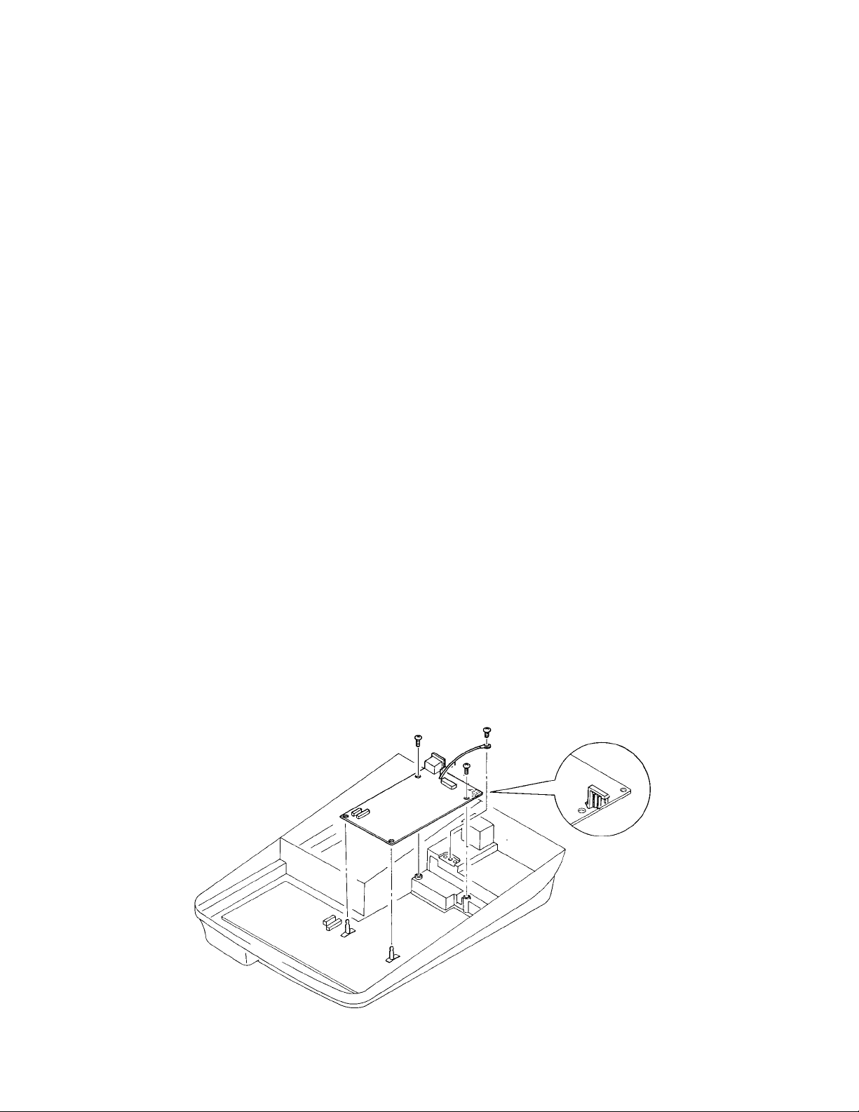
1. TO INSTALL THE I/O-PB-11 (for model CE-4700, TK-1300, TK-2300, TK-2700, TK-5100)
1) Plug of f t he A C c or d from outlet and turn the mo de s witch to REG m ode for
dis c har ge of elec trolyti c ca pacitors.
2) Open the upp er c as e and remov e the Ni- c d batter y c onnector. To open u pper
case, refer section 8 of disassembly in each ECR service manual.
3) In case of using scale, cut off the masking cover for scale.
4) Replace the ROM for necessary version.
5) Mount necessary RAM chips to main PCB.
6) Mount the two locking supporters on the PCB.
7) Connect the I/O-PB-11 and main PCB by two cables carefully caused the
cable lines ar e ver y nar r ow.
8) Connect the F.G. wire of I/O-PB-11 to the F.G. plate by screw.
9) Conne c t t he Ni-c d batter y c onnect or to the m ain PCB .
10) Perform the MAC operation and chec k whet her the machine is norm al condi-
tion .
11) Power off and close the upper case by screw.
In-line connector
— 1 —
Page 4
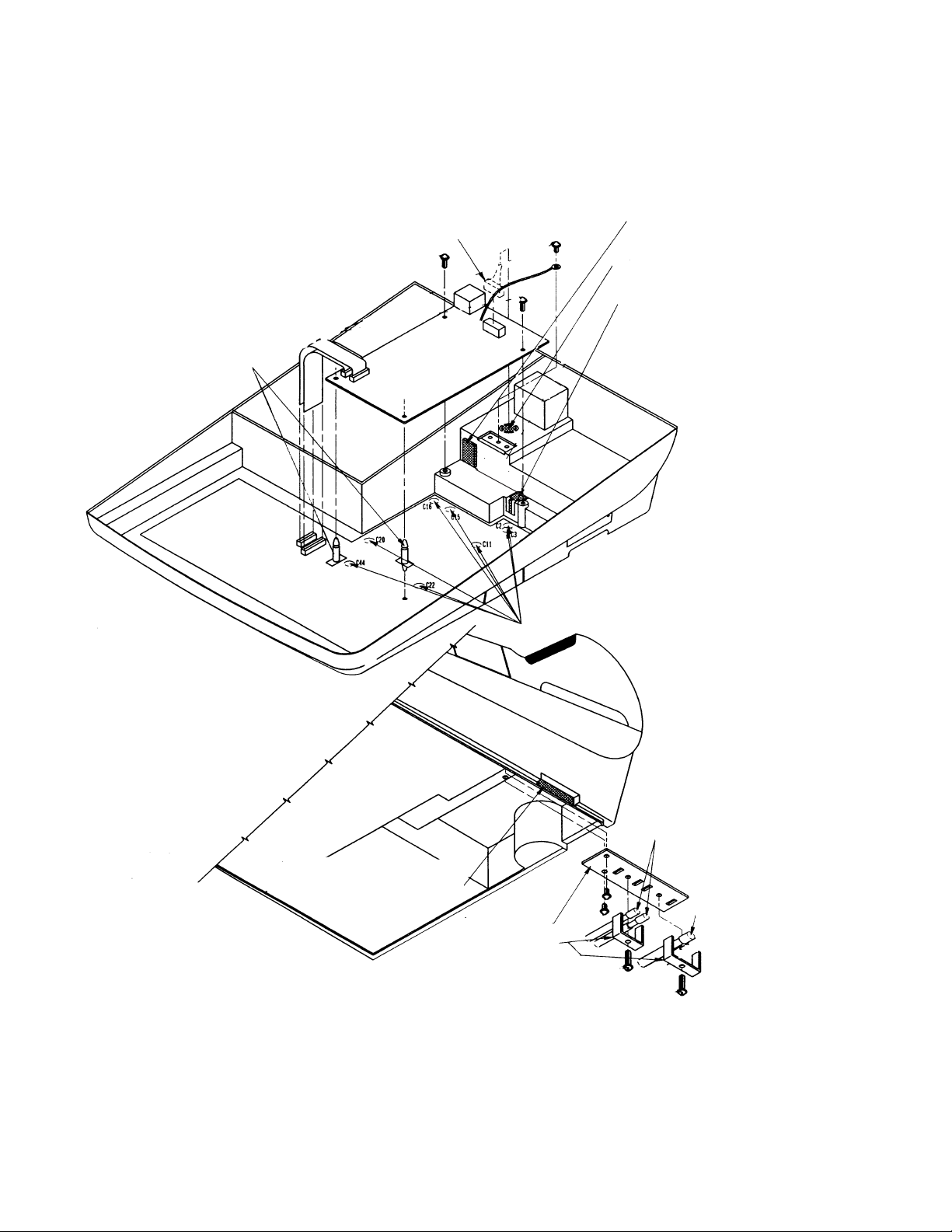
Scale cable
SCL-CB-10
Cut the masking cover for ON-line
connector.
Cut the masking cover for scale.
Cut the masking cover for In-line
connector
Locking supporters
I/O-PB-11
Check whether those capacitors are lying.
Cut the masking
part if necessary.
Cable fixing plate
Cable supporter
— 2 —
In-line cables
Scale cable
Page 5
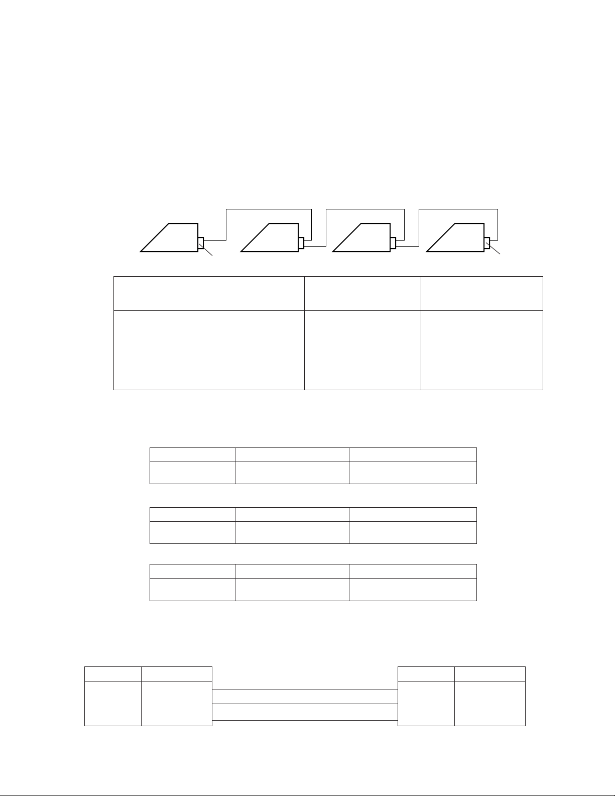
2. INTERFACE
2-1. C-In line (ECR to ECR)
1) C-In line connection diagram
The maximum C-In line cable length and the maximum connection unit will be
varied by the in-line communication speed as shown below list.
[C-In line cable wiring]
Master Satellite SatelliteSatellite
Terminater (100 ohms)
C-In line communication speed Maximum Maximum
(Baud rate) connection unit cable length A ( m )
1.25 M bps 8 86
625 K bps 12 200
312.5 K bps 20 430
156.25 K bps 32 890
Total cable length is max. A m
Terminater (100 ohms)
2) C-In line cable, Connector, and Terminater
C-In line cable
Code No. Parts name Specification
1904 4023 In-line cable IPEV-SLA0.5x1P
C-In line connector
Code No. Parts name Specification
3500 5820 In-line connector kit XLP-KIT-1
Terminater
Code No. Parts name Specification
2600 2516 Carbon film resistor R-25-100-J
3) Cable connection diagram
Signal Pin Signal Pin
SD 1 SD 1
RD 2 RD 2
FG FG plate FG FG plate
(Master side) (satellite side)
— 3 —
Page 6
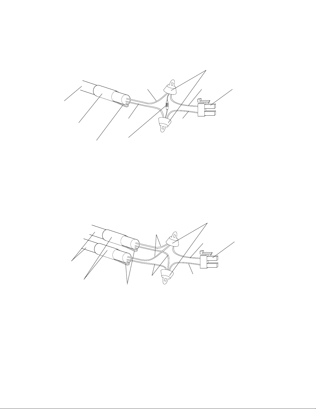
4) To fix C-In line connector to ECR.
Connect the C-In line cable and C-In line connector as shown below:
[Connector on the end of C-In line]
Terminal cap
C-In line cable
Wrap bent shield wire
with Copper tape.
Shield wire
[Connector between ECRs]
Red
Terminater (100 ohms)
Red
Red
BlackBlack
C-In line connector
Notes:
1.Use crimp tool for connecting terminal caps.
2.If crimp tool is not available, connect
the wires with solder instead of terminal cap. After the soldering, insulate
the wires with vinyl tape.
Terminal cap
C-In line cable
Wrap bent shield wire
with Copper tape.
Shield wire
Black
Red
Black
C-In line connector
Notes:
1.Use crimp tool for connecting terminal caps.
2.If crimp tool is not available, connect
the wires with solder instead of terminal cap. After the soldering, insulate
the wires with vinyl tape.
— 4 —
Page 7
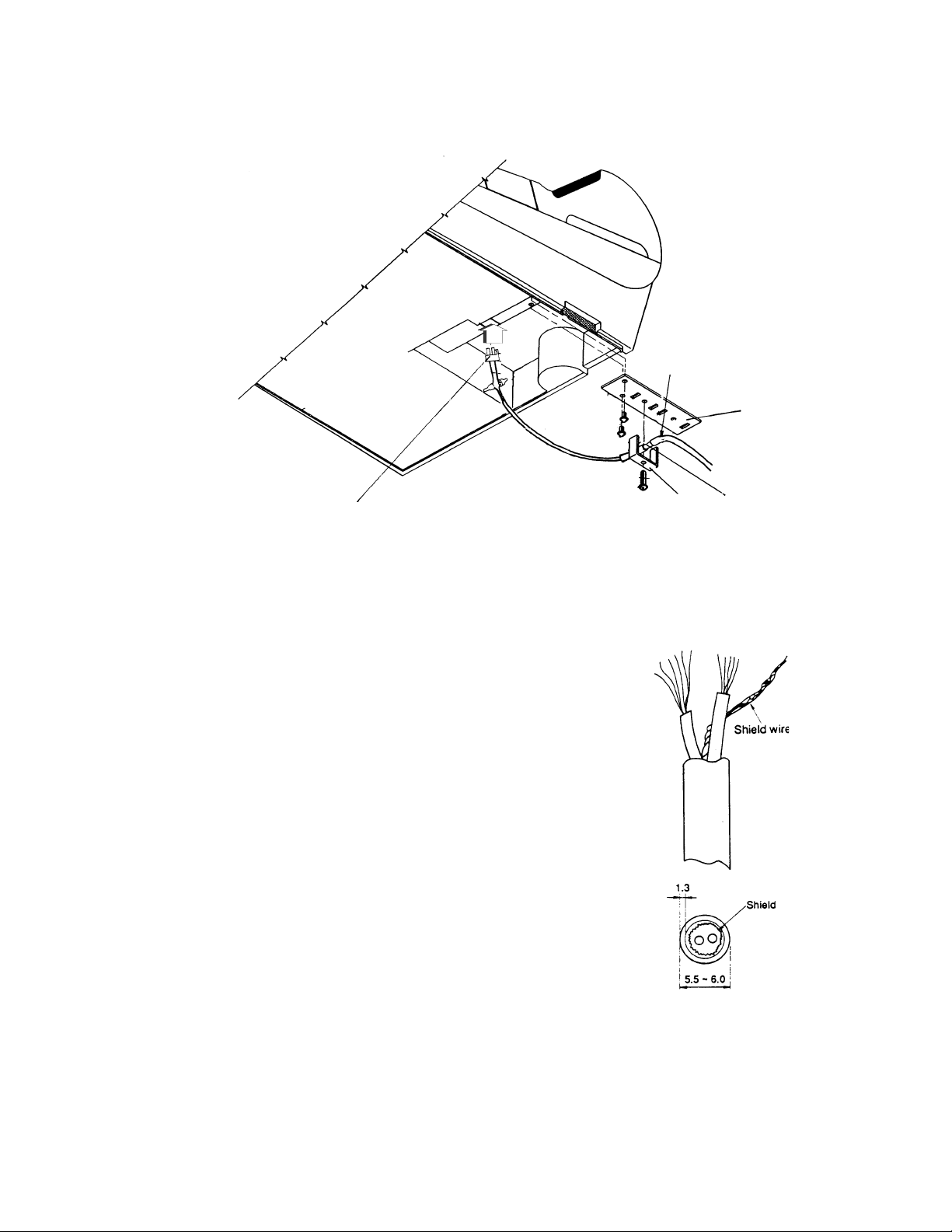
Connect the C-In line
connector as shown below:
C-In line cable
Cable fixing plate
Connect to C-In line connector.
6) C-In line cable specification
1. Structure
Conductor Material: Tin plated mild copper twist
Cross section area: 0.5mm
Construction: 20 pieces/0.18 mm
O.D. 0.95 mm
Insulation Material: Polyethylene
Thickness 0.3 mm
Sheath Material: PVC
Thickness 1.3 mm
Finished O.D.: 6.0 ~6.5 mm
Approx. weight: 55 kg/km
2. Properties (20°C)
Maximum conductor resistance 38.7 Ω/km
Minimum insulation resistance 10 kMΩ•km
Electric strength AC350 V/1 minute
Electrostatic capacity (Standard) 75 nF/km
2
Cable supporter
Part of copper tape
— 5 —
Page 8
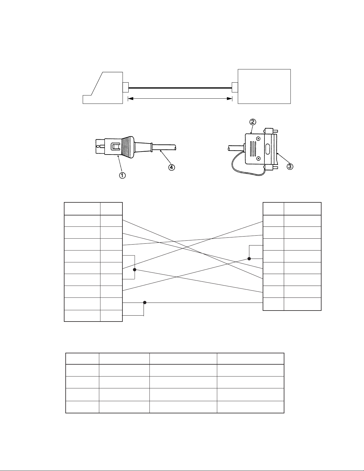
2-2. On line
(1) Direct connection to P/C
ECR
Cable length = Max. 15m
[Cable]
1) Wiring diagram (A) A SYNC.
PC-DOS
Personal
Computer
SIGNAL PIN
GND 1
ER 3
SD 4
RS 5
RD 7
CS 8
CD 9
DR 10
CI 13
2) Parts list
No. Code Number Part Specification
1 3612 0762 DIN 13P PLUG TCP9361-71-111
PIN SINGNAL
2SD
3RD
4RS
5CS
6DR
7SG
8CD
20 ER
2 3513 1019 Junction shell DB-C2-J9
3 3510 2043 Shell connector DB-25S
4 Cable PLGW-3456-01A
— 6 —
Page 9
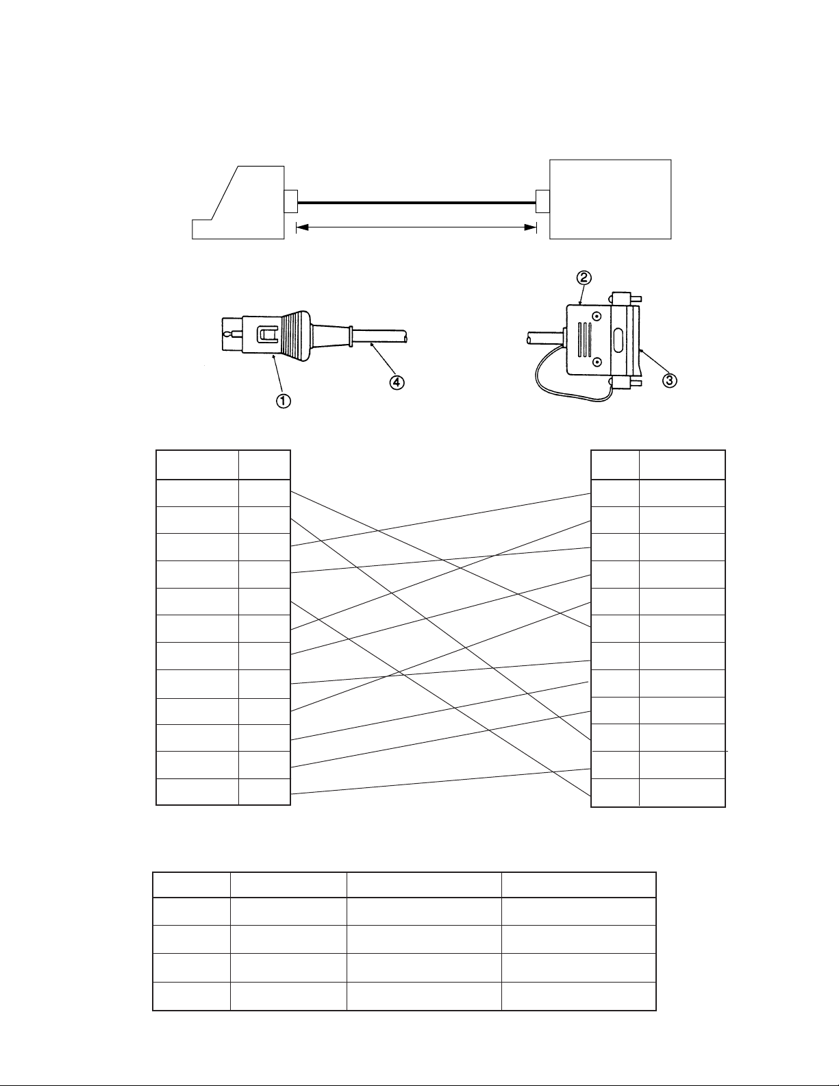
(2) MODEM connection
[Cable]
1) Wiring
SIGNAL PIN
ECR
GND 1
ER 3
SD 4
RS 5
MODEM
Cable length = Max. 15m
PIN SINGNAL
2SD
3RD
4RS
5CS
NC 6
RD 7
CS 8
CD 9
DR 10
NC 11
NC 12
2) Parts list
No. Code Number Part Specification
1 3612 0762 DIN 13P PLUG TCP9361-71-111
2 3513 1019 Junction shell DB-C2-J9
3 3510 2043 Shell connector DB-25S
4 Cable PLGW-3456-01A
CI 13
6DR
7SG
8CD
15 –
17 –
20 ER
22 CI
24 –
— 7 —
Page 10

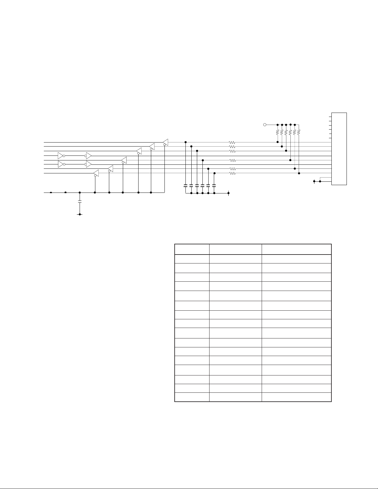
3. CIRCUIT EXPLANATIONS
D
0
3-1. Address selection
V+
C7
V-
GND
IC14
1
3
32
2
IC1
IC4
R2
2
3
IC4
R1
4
5
IC14
9
D7
10
D6
D5
D4
D3
D2
-12V
D1
D0
+12V
IC1
6
7
5
IC4
4
5
IC4
76
IC4
910
C8
C9
IC4
C10
12
11
C11
IC1
10
9
IC4
15
14
VCC
C23
GND
GND
GND
IRQ
GND
WR
GND
RD
GND
A7
GND
D6
GND
D5
GND
D4
GND
To E570-1To E570-1
D3
-12V
D2
-12V
D1
12V
D0
12V
GND
GND
GND
GND
VCC
VCC
IOCS
VCC
RESET
VCC
VCC
+12V
+
-12V
1
2
3
4
5
6
7
8
9
D7
10
11
12
13
14
15
16
17
18
19
20
21
22
23
24
C1 C6
+
R9
1
A3
2
R8
3
A2
4
R7
5
A1
6
R6
7
A0
8
9
10
R5
11
12
R4
13
14
R3
15
E
16
CS for IC10
(C-In line controller)
IC17
1
1G
2
1A
3
1B
4
1Y0
5
1Y1
6
1Y2
7
1Y3
8
GND
GND
VCC
16
VCC
15
2G
14
2A
13
2B
12
2Y0
11
2Y1
10
2Y2
9
2Y3
C31
IC12
11
13
IC14
12
R27
12
11
13
CLK for IC9
RDTM
IC14
4
6
5
8
IC12
IC12
IC15
C30
GND
C33
GND
4
IC15
1
2
4
5
10
IC15
11
IC12
2
1
3
IC15
9
3
VCC
8
10
C37
GND
R26
R25
D2
D3
GND
D4
D5
D6
D7
R10
C29
IC5
5
6
6
8
9
12
13
C32
IC16
1
Q12
2
Q6
3
Q5
4
Q7
5
Q4
6
Q3
7
Q2
8
GND
IC7
1
D2
2
D3
3
RXD
4
GND
5
D4
6
D5
7
D6
8
D7
9
TXCLK
10
WR
11
CS
12
C/D
13
RD
14
RXRDY
R11
16
VCC
15
Q11
14
Q10
13
Q8
12
Q9
11
RST
10
CLK
9
Q1
USART
28
D1
27
D0
26
VDD
25
RXCLK
24
DTR
23
RTS
22
DSR
21
RESET
20
CLK
19
TXD
18
TXEMP
17
CTS
16
SYNC
15
TXRDY
VCC
C36
GN
D1
D
According to the address of main CPU, the decorder selects the following optional devises.
IC No. Pin No. CPU address Descriptions
IC17 4 1Y0 0034H & RD="L" RDTM gate enable of IC8 (For scale data read)
10 2Y2 0036H Chip selection of C-In line controller
IC14 11 CLK 0034H & WR="L" Clock signal of IC9 (For C-In line controller data)
IC15 6 CS 0030H Chip selection of USART (Data)
0031H Chip selection of USART (Control status)
— 8 —
Page 11
D1
D2
D3
ENABLE
D0
CLOCK
D6
D7
RDTM
3-2. Scale buffer circuit
When a measured object is put on the scale, the scale starts weighing. During
weighing, MO signal is "H". When the weighing is finished with indication of the
weight of measures object, the MO signal becomes "L".
Then EN signal is output to the scale and the scale output the weight data
(D0~D3) to the scale buffer.
9
IC5 IC1
11
IC5
8
10 14
11
12
15
IC1
13
7
IC8
19
C19
14 6
1
515
19
IC8
1
NC
Vcc
1
2 3 4 5 6 7
1
GND
R13
R14
R15
R16
R17
R18
18 2
3
19
16 4
IC8
1
IC8
IC8
1
17
IC8
2 3 4 5 6 7
CA1
RA1
GND
2
3
4
5
6
7
8
9
10
11
12
13
14
15
16
NC
NC
NC
NC
NC
D1
D2
D3
ENABLE
D0
CLOCK
MOTION
RANGE
GND
GND
To E570-1
GND
Vcc
Vcc
Vcc
Pin description of scale connector
Pin No. Signal Name Descriptions
1 NC Non connection
2 NC Non connection
3 NC Non connection
4 NC Non connection
5 NC Non connection
6 NC Non connection
7 D1 Data
8 D2 Data
9 D3 Data
10 ENABLE Enable signal
11 D0 Data
12 CLOCK Clock signal
13 MOTION Motion signal
14 RANGE Out of range signal
15 GND GND
16 GND GND
— 9 —
Page 12
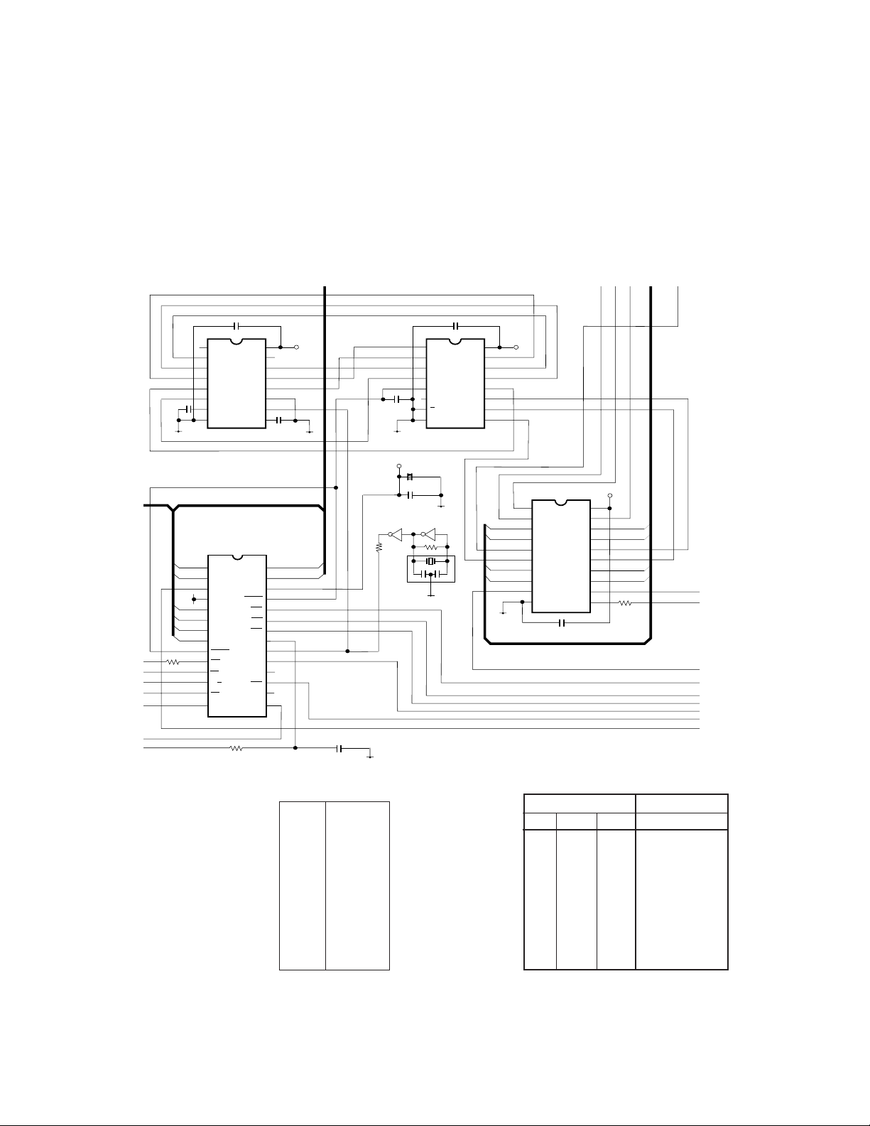
3-3. On line circuit (RS-232C)
1. Baud rate selection for On line (RS-232C)
Basic clock (307.2 KHz) is divided into seven clocks by binary counter IC16 and
they are supplied to D0~D6 terminals of multiplexer IC13. The IC13 outputs one
clock to USART according to the condition of select signals A, B, and C.
C32
IC16
1
Q12
2
Q6
3
Q5
4
Q7
5
Q4
6
Q3
C33
7
Q2
8
GND
GND
IC7
1
D2
D2
2
D3
D3
3
RXD
4
GND
D4
D5
D6
D7
R10
10
11
12
13
14
RXCLK
GND
5
D4
6
D5
7
D6
8
RESET
D7
9
TXCLK
WR
TXEMP
CS
C/D
SYNC
RD
TXRDY
RXRDY
VCC
RST
VCC
16
15
Q11
14
Q10
13
Q8
12
Q9
11
10
CLK
9
Q1
C36
GND
28
D1
27
D0
26
25
24
23
22
21
20
19
18
17
16
15
VDD
DTR
RTS
DSR
CLK
TXD
CTS
D1
D0
C38
GND
VCC
+
C21
C22
IC5
34
R36
3
C34
IC13
1
D3
2
D2
3
D1
4
D0
5
Y
6
W
7
G
8
GND
GND
IC5
12
R12
1
X1
2
GND
VCC
VCC
16
15
D4
14
D5
13
D6
12
D7
11
A
10
B
9
C
VCC
VCC
20
19
Q8
18
D8
17
D7
16
Q7
15
Q6
14
D6
13
D5
12
Q5
11
CLK
D2
D3
D4
D6
R19
IC9
1
CLR
2
GND
Q1
3
D1
4
D2
5
Q2
6
Q3
7
D3
8
D4
9
Q4
10
GND
C20
D1
D0
D5
D7
C5
R11
GND
Output of IC16
Q3 38.4 K
Q4 19.2 K
Q5 9,600
Q6 4,800
Q7 2,400
Q8 1,200
Q9 600
Q10 300
Truth table of IC13
Input Output
ABCY
LLLD0
HLLD1
LHLD2
HHL D3
LLHD4
HL HD5
LHHD6
HHHD7
— 10 —
Page 13

2. On line circuit (RS-232C)
13
12
11
10
9
8
7
6
5
4
3
2
1
CI
NC
NC
DSR
CD
CTS
RXD
NC
RTS
TXD
DTR
NC
GND
To ON-LINE
RA2
R21
GND
V-
C12
C13
1
3
6
8
11
7
14
2
4
5
9
10
12
13
Vcc
IC8
IC3
C14
C16
C15
C17
C18
321
654
8910
11
12
13
321
IC6
IC6
IC6
IC6
IC8
9
11
12 8
1
19
GNDGND
GND
V+ V-
GND
GND
The on line port (RS-232C) is controlled by the USART µPD71051 and
supported only asynchronous communication.
RDTM
D4
DSR
D6
CTS
RXD
DTR
RTS
TXD
Pin description of UPD71051C
Pin No. Signal Description
1,2,5~8, D0~D7 Data bus
27,28
3 RxDATA Receive data input
9 TxCLK Transmitter clock input
10 WR Write signal
11 CS Chip select signal Input
12 C/D Control or data change
13 RD Read signal
14 RxRDY Receive ready output
15 TxRDY Transmittor ready output
16 SYNC/BRK Syncronization/Break (Not used)
17 CTS Clear to send signal input
18 TxEMP Transmitter empty
19 TxDATA Transmit data output
20 CLK Clock input
21 RESET Reset input
22 DSR Data set ready signal input
23 RTS Request to send signal output
24 DTR Data terminal ready signal output
25 RxCLK Receiver clock input
26 VDD VCC(+5V) terminal
— 11 —
Pin description of on line connector
Pin No. Signal Description
1 SG Signal ground
2 NC Non connection
3 ER Equipment ready
4 SD Send data
5 RTS Request to send
6 NC Non connection
7 RD Receive data
8 CTS Crear to send
9 CD Carrier detect
10 DR Data ready
11 NC No connection
12 NC No connection
13 CI Calling indicator
Page 14

3-4. C-In line circuit
GND
C35
C27
C26
2
1
To IN-LINE
RD
SD
R34
R23
D4D3D5
D2 D1
F1
F2
R33
R22
R32
R35
Vcc
R30
C28
R20
IC11 16
4
15
12
9
5
8
13
14
11
10
7
6
R31
R21
GNDGND
Vcc
Vcc
Vcc
A0
A1
A2
D0
D1
D2
D3
D4
D5
D6
D7
GND
VCC
RD
WR
CS
INTR
RST
TXEN
RXIN
TXOUT
X2
X1
GND
C3
C39
X2
R28
R29
1
2
3
4
5
6
7
8
9
10
11
12
24
23
22
21
20
19
18
17
16
15
14
13
C25
C24
+
TXOUT
RXIN
TXEN
IC10
D0
D1
D2
D3
D4
D5
D6
D7
Vcc
GND
1. C-In line controller (COM20020B)
IC10
1
A0/MUX
2
A1
3
A2/ALE
4
AD0
5
AD1
6
AD2
7
D3
8
D4
9
D5
10
D6
D7
11
GND
12
VCC
RD/DS
WR/DIR
INTR
RESET IN
TXEN
RXIN
PULSE2
PULSE1
XTAL2
XTAL1
24
23
22
CS
21
20
19
18
17
16
15
14
13
AD0~AD2,
D3~D7
RESET IN
A0/MUX
A1
A2/BALE
INTR
RD/DS
WR/DIR
CS
— 12 —
ADDRESS
DECODING
CIRCUITRY
STATUS/
COMMAND
RESET
LOGIC
BUS
ARBITRATION
CIRCUITRY
RECONFIGURATION
TIMER
2K X 8
RAM
MICROSEQUENCER
AND
WORKING
REGISTERS
ADDITIONAL
REGISTERS
TX/RX
LOGIC
OSCILLATOR
NODE ID
LOGIC
PULSE1
PULSE2
TXEN
RXIN
Page 15

2. COM20020B pin description
Pin No. Name In/Out Status Status Status Description
of OFF of ON of ON
No Token Token
1 A0/MUX In L L Pulse
2 A1 In L L L
3 A2/ALE In L L L
4 AD0 In/Out L Pulse Pulse
5 AD1 In/Out L Pulse Pulse
6 AD2 In/Out L Pulse Pulse
7 D3 In/Out L Pulse Pulse
8 D4 In/Out L Pulse Pulse
9 D5 In/Out L Pulse Pulse
10 D6 In/Out L Pulse Pulse
11 D7 In/Out L Pulse Pulse
12 GND Power GND GND GND
13 XTAL1 In L Pulse Pulse
14 XTAL2 In L Pulse Pulse
15 PULSE1 Out L H Pulse
16 PULSE2 Out L L L
17 RXIN In L H Pulse
18 TXEN Out L L Pulse
19 RESET IN In L H H
Input. On a non-multiplexed bus,
these signals are dirctly connectoed to
the low bits of the host address bus.
On a multiplexed address/data bus,
A0/MUX is tied low, A1 is left open,
and A2 is tied to the address latch
enable signal of the host. A1 is
connectoed to an internal pull-up
resistor.
Input/Output. On a non-multiplexed
bus, these signals are used as the
data lines for the device. On a
multiplexed address/data bus,
AD0~AD2 act as the address lines
(latched by ALE) and as the low data
lines for the device. D3~D7 are
always used for data only. These
signals are connected to internal pullup resistors.
Signal ground.
An external crystal shoul be connected
to these pins. If an external TTL clock
is used instead, it must be connected
to XTAL1 with a 390 ohms pull-up
resistor, and XTAL2 should be left
floating.
Output. In normal mode, these active
low signals carry the transmit data
information, encoded in pulse format,
from the COM20020 to the media
driver circuitry. When the device is in
backplane mode, the PULSE1 signal
driver is programmable (push/pull or
open-drain), while the PULSE2 signal
provides a clock with frequency of
crystal/4. PULSE1 is connected to a
week internal pull-up resistor in
backplane mode.
Receive input. This signal carries the
receive data information from the line
receiver circuitry to the COM20020.
Transmit Enable output. This signal
used in backplane mode to enable the
line drivers for transmission. The
polarity of the signal is programmable
by grounding the PULSE2 pin. This
option is valid only in backplane mode.
Input. This active low signal issued by
the microcontroller executes a hardware reset. It is used to activate the
internal reset circuitry within the
COM20020.
— 13 —
Page 16
Pin No. Name In/Out Status Status Status Description
of OFF of ON of ON
No token Token
20 INTR Out L H Pulse
Interrupt output. This active low signal
is generated by the COM20020 when
an enabled interrupt condition occurs.
INTR returns to its inactive state when
the interrupt status condition or the
corresponding interrupt mask bit is
reset.
21 CS In L H Pulse
Chip select input. This active low
signal issued by the microcontroller
selects the COM20020 for an access.
22 WR/DIR In L Pulse Pulse
Input. On a 68XX-like bus, this signal
is issued by the microcontroller as the
Read/Write signal to determine the
direction of data transfer. In this case,
a logic "1" selects a read operation,
while a logic "0" selects a write operation. In this case, data is actually
strobed by the DS signal. On an
80XX-like bus, this active low signal is
isuued by the microcontroller to
indicate a write operation. in this
case, a logic "0" on this pin, when the
COM20020 is accessed, enables data
from the data bus to be written to the
device.
23 RD/DS In L L Pulse
Read/ Data strobe signal input. On a
68XX-like bus, this active low signal is
issued by the microcontroller as the
data strobe signal to strobe the data
onto the bus. On a 80XX-like bus, this
active low signal is issued by the
microcontroller to indicate a read
operation. In this case, a logic "0" on
this pin, when the COM20020 is
accessed, enables data from the
device to the data bus to be read by
the microcontroller.
24 VCC Power GND +5V +5V
Power supply +5V.
— 14 —
Page 17

4. DIAGNOSTIC OPERATIONS
4-1. To start the diagnostic operation
START
Set mode switch to OFF mode.
While pressing the feed key, turn the mode switch to PROGRAM.
Release the feed key after 2 seconds. (Display shows all "0".)
Input following 10 digits number.
9 9 9 9 9 0 0 0 0 0 (Fixed value)
Press #2 key (Refer the each service manual for the key location.)
The machine prints initial message and issues the receipt.
To each test operation
The test mode starts by the above operations. And with this operation, the ROM sum
check is done automatically and the result is printed on the receipt. To return the normal
operation mode, perform the MAC (INIT1) operation.
NOTE: Please refer the each service manual for the following test operations:
1 Numeral keys check (0~9 keys)
2 General keys (All keys except Clear, paper feed, and numeral keys)
3 Switch check
4 I/O Port status check
5 General test (RAM, display, printer, drawer 1, clock, auto cutter)
6 RAM read after write test
7 RAM read only test
8 RAM card read after write test
9 RAM card read only test
10 Display check
11 Time and date test
12 Printer check
13 Slip printer check
14 Centronic printer check
15 Drawer check
16 Auto paper cutter check
17 On line loop back test
18 Scale reading test
— 15 —
Page 18

4-2. Check Items for I/O-PB-11
1 C-In line ID No. & Baud rate set (High speed in-line talken start command)
2 C-In line test termination (Termination command)
3 C-In line CN (connection) type message transmission test
4 C-In line CN (connection) type message reception test
5 C-In line CL (connection less) type message transmission test
6 C-In line CL (connection less) type message reception test
7 C-In line control chip status check
4-3. Operations
1. C-In line ID No. & Baud rate set (High speed in-line talken start command)
[Operation]
Press 8 0 n #2 . (whereas n = Machine ID No.)
Press 8 1 m #2 . (whereas m = Baud rate code)
The baud rate code is as follow:
m = 0; 156.25 K bps. m = 2; 625 K bps.
m = 1; 312.5 K bps. m = 3; 1.25 M bps.
Note 1: To stop the test, perform Termination command.
Note 2: Select ID No. from 1 to 32 for test operation.
Note 3: To set the 2 digits ID No., operate as follows:
Press 8 0 0 #2 .
Press n n #1 . (whereas n n = Machine ID No. more than 2 digits.)
ID No. = 10 ~ 32.
Press 8 1 m #2 . (whereas m = Baud rate code)
[Print sample]
800 OK 01
814 OK
ID No.
— 16 —
Page 19

2. C-In line test termination (Termination command)
This command is for the termination of the TOKEN.
[Operation]
Press 8 2 0 #2 .
[Print sample]
820 OK
3. C-In line CN (connection) type message transmission test
This command will check the communication by CN type message. This operaton
will compare with transmission data and reception data after sending data to the
reception machine.
Before performing this transmission test, set the ID No. & Baud rate by the Item
No.1 operation.
[Operation]
Press 8 3 n #2 . (whereas n = Machine ID No.)
ID No. = 0 ~ 9 (ID No.0 is for the host computer.)
(10~32 are not possible to use.)
Note 1: To stop the test, press #2 key.
Note 2: To perform this test, the reception machine is necessary. Before operat-
ing this test, perform the CN type receprion command on the reception
machine.
[Print sample (Normal end) ]
831 OK
— 17 —
[Print sample (Abnormal end) ]
831 ER83 01-0000
Error code
Error block counter No.
Error machine ID No.
Page 20
4. C-In line CN (connection) type message reception test
This command will check the communication by CN type message. This operaton
will return the transmission data after reception data without any change.
Before performing this transmission test, set the ID No. & Baud rate by the Item
No.1 operation.
[Operation]
Press 8 4 n #2 . (whereas n = Machine ID No.)
ID No. = 1 ~ 9(ID No.0 is for the host computer.)
(10~32 are not possible to use.)
Note 1:To stop the test, press #2 key.
Note 2:To perform this test, the reception machine is necessary.
After operat ing this test, perform the CN type transmission command
on the transmission machine.
[Print sample (Normal end) ]
841 OK
[Print sample (Abnormal end) ]
841 ER83 01-0000
Error block counter No.
Error code
Error machine ID No.
5. C-In line CL (connection less) type message transmission test
This command will check the communication by CL type message. This operaton
will send the data to the all reception machines.
Before performing this transmission test, set the ID No. & Baud rate by the Item
No.1 operation.
[Operation]
Press 8 5 0 #2 .
Note 1: To stop the test, press #2 key.
Note 2: To perform this test, the reception machine is necessary. Before operat
ing this test, perform the CL type receprion command on the reception
machine.
— 18 —
Page 21

[Print sample (Normal end) ]
[Print sample (Abnormal end) ]
850 OK
6. C-In line CL (connection less) type message reception test
This command will check the communication by CL type message. This operaton
will receive the transmission data.
Before performing this transmission test, set the ID No. & Baud rate by the Item
No.1 operation.
[Operation]
Press 8 6 0 #2 .
850 ER83 01-0000
Error code
Error block counter No.
Error machine ID No.
Note 1: To stop the test, press #2 key.
Note 2: To perform this test, the Transmission machine is necessary.
After operating this test, perform the CL type transmission command on
the transmission machine.
[Print sample (Normal end) ]
860 OK
7. C-In line control chip status check
This command will check the C-In line control chip status. When the 4 digits of left
side are displayed "0111", the C-In line control chip is working normally.
[Display]
[Print sample (Abnormal end) ]
860 ER83 01-0000
Error block counter No.
Error code
Error machine ID No.
0 1 1 1 0 0 10
{
Normal condition
— 19 —
Page 22

8. Diagnostic program error code
Error Nature of error Function Details
Code code
01 ROM check sum error At power on When the diagnostic program is started up, the last 2 digits of
the ROM's check sum is not 00.
02 RAM write error 10 Test data cannot be written in the RAM.
(1 byte read after write error)
03 RAM read error 10, 12 Data error at RAM data reading
04 RAM card write error 14 Test data cannot be written in the RAM card.
(1 byte read after write error)
05 RAM card read error 14,16 Data error in the RAM card reading check
06 Non connection error 14 RAM card is not installed. Or, a ROM card is installed in the
of RAM card RAM card test.
(ROM card connection)
10 Abnormal voltage of 40 Monitor terminal of drawer PCB receives BUSY signal for
drawer power. more than 1 second.
12 BUSY time out at 50, 51 Data cannot be sent due to no reception of BUSY signal.
In-line data transmission (USRT hardware error)
13 In-line receive time out 52, 53 In-line receive test is compulsorily stopped by #2 key.
14 ON-line transmission 54, 55 Data cannot be sent due to no reception for BUSY signal.
BUSY time out (Hardware error)
15 On-line receive time out 55 Cannot receive loop-back data
16 In-line/On-line receive 50~55 A parity error in received data
parrity error.
17 In-line/On-line receive 50~55 A framing error in received data
framing error
18 In-line/On-line receive 50~55 Received data is not correct.
data error
19 On-line CI signal error 54, 55 Poor connection or no connection of loop back connector.
Abnormal CI signal.
20 On-line CD signal error 55 Poor connection or no connection of loop back connector.
Abnormal CD, RTS lines (On-line 2).
21 On-line DR/CTS signal 54, 55 Poor connection or no connection of loop back connector.
error Abnormal CTS (On-line 1), DR (On-line 2).
— 20 —
Page 23

Error Nature of error Function Details
Code code
24 KB-1 time-out error 70 An error occurred during test of KB-1.
25 KB-1 reception error 70 An error occurred while reading data of KB-1.
28 Scale data error 71 An error occurred while reading scale data.
29 Thermal printer board 36, 37 An error occurred in the thermal printer board.
error
30 Thermal printer paper 36, 37 No paper in the thermal printer.
out error
64 AUTOPGM or X/Z error - A different format data is received.
(100)
65 AUTOPGM or X/Z error - A different format of compressed data is selected.
(101)
66 AUTOPGM or X/Z error - A received compressed data is abnormal.
(102)
67 AUTOPGM or X/Z error - A received compressed data is abnormal.
(103)
68 AUTOPGM or X/Z error - Auto program code 90/93 is received from different model.
(104)
69 AUTOPGM or X/Z error - Auto program code 90 is received from bigger memory ECR.
(105)
6A AUTOPGM or X/Z error - Abort.
(106)
6B AUTOPGM or X/Z error - A disk error of PC side.
(107)
6C AUTOPGM or X/Z error - A communication sequence is abnormal.
(108)
77 RAM card error - A power failue happened during read or write operation.
(119)
78 RAM card error - The RAM card door opened during read or write operation.
(120)
79 RAM card error - RAM card is not installed.
(121)
7A RAM card error - A ROM card is installed.
(122)
7B RAM card error - A different RAM card is installed.
(123)
7C RAM card error - A write operation is performed in the RAM card which has
(124) already some data.
7D RAM card error - A read operation is performed in the empty RAM card.
(125)
7E RAM card error - Write protect switch is on in the RAM card.
(126)
7F RAM card error - The other error. (Abnormal condition)
(127)
NOTE: The number of shown in the () is the operation error code number after code E56- of system error.
— 21 —
Page 24

Error Nature of error Function Details
Code code
80 C-in line controller error 81,83,84,85,86 Reset error of C-In line controller
(128)
81 C-in line controller error 81,83,84,85,86 Receive interruption operation is not finished.
(129)
82 C-in line controller error 81 Initial error of controller. The ID No. and start up operation
(130) is not finished yet.
83 C-in line controller error 82,83,84 Token signal can not be received by some reason. Or, there
(131) are no machine in C-In line cable.
84 C-in line controller error - Transmission size is over.
(132)
85 C-in line controller error 83,85 The transmission is not finished by a noise or some reasons.
(133)
86 C-in line controller error 81 The same ID No. exists on the C-In line cable.
(134)
87 C-in line controller error - The machine does not enter the network caused a mismatch of
(135) the baud rate or some reasons.
90 C-In line protocol error 83,84,85,86 NCB (Network control block) open parameter mismatch
(144) or memory over error
91 C-Inline protocol error - NCB open error (Not used)
(145)
92 C-Inline protocol error - NCB close error (Not used)
(146)
93 C-Inline protocol error - NCB connection error (Not used)
(147)
94 C-Inline protocol error - NCB operation check error (Not used)
(148)
95 C-Inline protocol error - Header packet not received error (Not used)
(149)
96 C-Inline protocol error - NCB connection error (Not used)
(150)
97 C-Inline protocol error - NCB non connection error (Not used)
(151)
98 C-Inline protocol error - NLib(Network library) parameter mismatch error
(152)
99 C-Inline protocol error - Transmission retry over error
(153)
9A C-Inline protocol error - Reception retry over error
(154)
9B C-Inline protocol error 83,84 Packet block number mismatch error
(155)
9C C-Inline protocol error 83,84 NCB does not exist. Or, the NCB application software is
(156) stopped.
9D C-Inline protocol error 83,84 Reception memory over error.
(157)
9E C-Inline protocol error 83,84 Transmission retry over error. (Time over)
(158)
9F C-Inline protocol error 83,84 The receprion complete packet is not returned from terminal.
(159)
NOTE: The number of shown in the () is the operation error code number after code E56- of system error.
— 22 —
Page 25

Error Nature of error Function Details
Code code
A0 C-Inline protocol error - Reception application program is busy at the other terminal.
(160)
A1 C-Inline protocol error 83 The ID No. does not exist in the network.
(161)
B0 XMODEM protocol error - DSR signal does not turn on even ER signal turns on at the
(176) open time.
B1 XMODEM protocol error - An abnormal data is received.
(177)
B2 XMODEM protocol error - Trigger packet is not received.
(178)
B3 XMODEM protocol error - ACK packet is not received.
(179)
B4 XMODEM protocol error - NAK transmission over error.
(180)
B5 XMODEM protocol error - DSR signal turns off. (The line connection is terminated.)
(181)
B6 XMODEM protocol error - CAN (Cancel) data is received.
(182)
B7 XMODEM protocol error - EOT (End of text) data does not receive.
(183)
B8 XMODEM protocol error - CD signal does not turn on. (The connection is not completed.)
(184)
C0 Resource error - QCB is not existed.
(192) (QCB=Que control block=Send /Receive buffer control area)
C1 Resource error - QCB buffer area is already existed.
(193)
C2 Resource error - QCB buffer area is already released.
(194)
C3 Resource error 83,84,85,86 TMCB (Timer control block) is not existed.
(195)
C6 Resource error 83,84,86 Reception time out error.
(198)
NOTE: The number of shown in the () is the operation error code number after code E56- of system error.
— 23 —
Page 26

5. ERROR CODE LIST
Error codes appear on the display whenever you make a mistake during operations.
Error
Code
E01
Meaning
Operation without entering PROGRAM, X1,
or X
mode secret code (PASSWORD).
2/Z2
Action
Enter secret code (PASSWORD).
Dot
Display
PASSWORD
E02
E03
E04
E05
E06
E07
E08
E09
E10
E11
Registration without entering clerk secret
number.
Incorrect initialization or unit lock clear operation.
MODE switch position changed before finalization.
Operation error. (One shot error)
Clerk button pressed before finalization of a
registration being performed under another
clerk button.
Receipt ON/OFF button setting changed before finalization under another setting.
Registration without entering number of customers.*
Finalization of a transaction attempted without registration of the tax.*
Finalization without confirmation of subtotal.*
FS/TEND key pressed without first pressing
the FS/ST key.
Enter clerk secret number.
Perform initialization or unit lock clear
operation again.
Return MODE switch to original setting
and finalize operation.
Operate next correct operation.
Press the original clerk button and final-
ize the registration before pressing another clerk button.
Return receipt ON/OFF switch to its original setting and finalize registration.
Enter number of customers.
Register the tax.
Press SUBTOTAL key.
Press the FS/ST key.
ERR CLK#
START
ERR MODE
OPE ERROR
ERR CLERK
RECEIPT SW
ERR CUST
ERR TAX
ERR ST
ERR FSST
E12
E13
E14
E16
E17
E18
E19
E20
Two consecutive transactions attempted in
refund mode.*
Validation not performed.
READ/RESET operation without declaration
of money in drawer.*
Journal memory data is not found.
Registration while ECR drawer is open.*
Change amount exceeds preset limit.*
Contents of drawer exceed programmed limit
(sentinel function).*
Slip printing not perfomed.*
Switch to another mode and then back to
RF mode for next transaction.
Perform validation operation.
Perform money declaration.
Input correct date and consecutive No.
Shut drawer before registration (when
optional compulsory drawer is used.)
Re-enter amount tendered.
Arrange to have contents of drawer picked
up by management.
Perform slip printing operation.
RF MODE
VALIDATION
DECLARE
NOT FOUND
DRAWER
CHANGE
OVER
INDW OVER
SLIP
Note: (*) These errors will only be generated when the respective functions are
programmed as being compulsory or prohibited.
— 24 —
Page 27

Error
Code
E21
Meaning
Actual stock quantity less than or equal to
minimum stock quantity.
Action
Perform stock maintenance.
Dot
Display
MIN. STOCK
E22
E23
E24
E25
E26
E27
E28
E29
E30
E31
Negative value for actual stock quantity.
Check endorsement printing not performed.*
Scale data cannot be read due to data variation or scale is turned off.
Finalize operation attempted without entering amount tendered.
Memory allocation exceeds total ECR RAM
capacity.
No thermal printer paper.
A different clerk operated the ECR without
pressing HOLD key.*
Attempt to register without printing a check.*
Attempt to register without entering a check
number.
Attempt to register without entering a table
number.
Perform stock maintenance.
Perform check endorsement printing operation.
Press C key or turn the scale on.
Enter amount tendered.
Reallocate without exceeding RAM capacity.
Add thermal printer paper.
Press HOLD key before signing in.
Finalize the transaction by printing a check
with the slip printer.
Enter a check number
Enter a table number first then register.
- STOCK
CHK ENDORSE
ERR SCALE
TENDER
MEMORY OVER
NO PAPER
HOLD
CHK PRINT
ERR CHECK#
ERR TABLE#
E32
E33
E34
E35
E36
E37
E38
E39
The detail memory of the check tracking
system is full.
Attempt to use the same check number which
already exists.
Attempt to proceed operation with entering a
non-existing check number.
A different type of RAM card is used.
Attempt a registration without entering number
of condiment.*
Attempted to register check tracking items
without print.*
Journal memory data read error.
Journal memory full.
Use the NB key to finalize the transaction
of the check.
Finalize transaction with the number or
use a different check number.
Re-enter an existed check number then
perform operation.
Use proper type of RAM card.
Register number of condiments.
Finalize transaction with printing all the
check tracking items.
Hard error. Check RAM chip.
Liquidate the ECR (issuing Z report).
MEMORY FULL
OCCUPIED
NOT FOUND
ERR CARD
CONDIMENT
GUEST RCT
J-MEMO ERR
J-MEMO FULL
Note: (*) These errors will only be generated when the respective functions are
programmed as being compulsory or prohibited.
— 25 —
Page 28
Error
Code
Meaning
Action
Dot
Display
E41
E42
E44
E45
E46
E47
E48
E49
E50
E51
E52
Kitchen printer down error.
Kitchen printer paper near end error.
Kitchen printer buffer error.
Separate Item error.
Time attendance memory full error.
The number of clerk for Time Attendance is
not found.
The number of clerk for Time Attendance is
already entered.
A data exists in the data collection memory
area.
P/C is down.
IDC buffer near end/ full error.
Kitchen printer buffer (P/C side) full error.
Check the power of the kitchen printer.
Change the roll paper to new one.
The over data is printed on the receipt
paper automatically.
Input the correct item checking by the
Slip/ Guest receipt.
Make Z report of time attendance.
Input the correct number for Time Attend-
ance.
Input the correct number for Time Attend-
ance.
Clear the data in the collection memory
area.
Start up the P/C again.
Make Z operation od IDC area.
The over data is printed on the receipt
paper automatically.
KP ERROR #n
KP PAPER #n
KP BF OVER
INCMPLT MENU
MEMORY FULL
NOT FOUND
OCCUPIED
TENDER
**PC STOP**
IDC FULL
KP FULL
E53
E54
E55
E56-XXX
E57
E58
E59
Kitchen printer print compulsory error.
The check number is used.
The same ID number exists in the net work.
Net work system error. The number XXX is
the diagnostic error code. Refer the error
code list on page 20 ~ 23.
SA-3000 CPU's UPS is working.
Hotel host P/C down error.
ID number/ Baud rate change alarm.
Perform the kitchen printer print operation
before the other operation.
Input the correct number of check number.
Set the correct ID number.
From the error diagnostic error code ,
perform the necessary action.
Check the P/C (SA-3000) power failure.
The communication error. The transfered
data is lost. No operation is necessary.
First, set the ID No. & baud rate value to 0.
Then, turn power off and on. Set the
necessary value of the ID No. & baud rate.
ERR KP PRINT
BUSY
DUPLICATE ID
SYSTEM ERROR
NOT FOUND
PC/IRC ERROR
ID/BAUD CORR
Note: (*) These errors will only be generated when the respective functions are
programmed as being compulsory or prohibited.
— 26 —
Page 29

6. IC DATA
TC74HC4050AP
(TOP VIEW)
TC74HC02AP
4B
4A
1213
11
4YVDD
14
TC74HC00AP
QUAD 2-INPUT NAND GATE
(TOP VIEW)
TC74HCU04AP
HEX INVERTER
(TOP VIEW)
TC74HC244AP
3B3Y
3A
8910
1
1Y 1A
34 567
2
1B
(TOP VIEW)
TC74HC139AP
(TOP VIEW)
2Y
2A2BVSS
(TOP VIEW)
INPUTS
ENABLE
SELECT
OUTPUTS
G B A Y0 Y1 Y2 Y3 OUTPUT
HXX HHHH NONE
LLL LHHH Y0
LLHHLHH Y1
LHL HHLH Y2
LHH HHHL Y3
X: Don't care
SELECTED
— 27 —
Page 30

TC74HC273AP
OCTAL D-TYPE FLIP FLOP WITH CLEAR
(TOP VIEW)
TC74HC4049AP
INPUTS OUTPUT
CLEAR D CLOCK Q FUNCTION
L X X L Clear
HL L –
HH H –
H X Qn No change
(TOP VIEW)
TC74HC4040AP
(TOP VIEW)
— 28 —
Page 31

TC74HC151AP
(TOP VIEW)
SN751178N
(TOP VIEW)
SN75188N
(TOP VIEW)
SN75189AN
(TOP VIEW)
— 29 —
Page 32

7. PARTS LIST
— 30 —
Page 33

— 31 —
Page 34
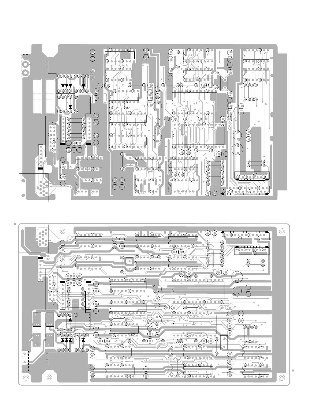
8. PCB LAYOUT
12
CN2
RA2
13
12
R23
R22
R21
D1
R20
F2
74HC151
R36 C33
C34
IC13 IC16
74HC4049
74HC4040
R29
IC4
IC1
C35
R10
R11
C10
R28
C3C4
COM20020BIP
C5
IC7
C8
R9
R8
R7
R6
R5
R4
R3
2
1
C36 C37
X2
C6
2
1
74HC139
C32
IC17
R35D5D4D3R34
F1
15
16
R33D2R32
R18
R17
R16
R15
R14
R13
C29
C30 C31
74HC00
C28
R19
IC9IC8
74HC273
IC14
R31
SN751178
IC11
C26
C27
C25
R30
+
IC10
C24
C23
C22
+
CN3
RA1
1
2
FG
8
4
C14 C15
CN11
C16
C18
C17
SN75189
SN75189
CA1
C19 C20
IC6IC3
74HC244
R12
C13
C12
74HCU04
VCC
IC5
X1
SN75188
C13 C13
IC2
GND
C21
µPD71051C
IC4
74HC4050
C11
+
74HC02
C2
+
CN4
R27
C7
CN5
74HC00
R26
R25
C1
R24
IC12 IC15
R2
R1
16
15
24
23
CN2
1
CN1
8
4
13
12
FG
2
1
RA2
RA1
CN3
16
15
F1
F2
R20
12
D1
R21
R22
R23
R35D5D4D3R34
C15 C14
C16
C17
SN75189
SN75189
C18
CA1
R13
R14
R15
R16
R17
R18
R33D2R32
C29
C30C31
IC6 IC3
C20 C19
R19
C28
74HC00
IC8
IC9
C13
R12
74HC244
74HC273
74HC139
C12
SN751178
IC2
–12V
+12V
SN75188
IC5
GND
X1
74HCU04
VCC
+
+
C26
IC11
IC14
R31
IC17
C35
C27
C25
C11
74HC4050
C21
µPD71051C
C22
C23
C24
IC10
R30
74HC4049
C9
IC13
C34
R36
IC16
C33
R29
74HC151
74HC4040
IC1
IC4
R10
C35
R11
C10
1
2
R3
R4
R5
R6
R7
R8
R9
C8
C5
COM20020BIP
R28
CN4
23
R24
24
15
16
R1
R2
IC12IC15
CN5
1
2
C7
+
C6
+
C1
C2
R27
R26
R25
X2
C36
74HC02
C37
74HC00
— 32 —
— 32 —
Page 35

9. CIRCUIT DIAGRAM
ABCDEFGH
1
+
C24
A0
A1
A2
D0
D1
D2
D3
D4
D5
D6
D7
GND
IC10
C25
VCC
INTR
RST
TXEN
RXIN
TXOUT
24
VCC
23
RD
WR
CS
X2
X1
R29
22
21
20
19
18
17
16
15
R28
14
13
X2
C39
C3
TXEN
RXIN
TXOUT
IC17
1
1G
1A
1B
1Y0
1Y1
1Y2
1Y3
GND
VCC
2G
2A
2B
2Y0
2Y1
2Y2
2Y3
C31
2
3
4
+12V
+
C7
2
-12V
V+
V-
5
6
7
8
GND
VCC
16
15
14
13
12
11
10
9
IC12
11
13
12
R27
IC14
12
11
13
D0
D1
D2
D3
D4
D5
D6
D7
1
2
3
4
5
6
7
8
9
10
11
12
GND
1
2
D0~7
RDTM
1
GND
2
GND
3
IRQ
4
GND
5
WR
6
GND
7
RD
8
GND
9
3
4
D7
GND
D6
GND
D5
GND
D4
GND
To E570-1
D3
-12V
D2
-12V
D1
12V
D0
12V
10
11
12
13
14
15
16
17
18
19
20
21
22
23
24
C1 C6
1
A3
2
GND
3
A2
4
GND
5
A1
6
GND
7
A0
8
GND
9
VCC
5
To E570-1
RESET
VCC
IOCS
VCC
VCC
VCC
10
11
12
13
14
15
E
16
GND
IC14
1
3
32
IC1
R2
3
R1
5
-12V
+12V
+
R9
R8
R7
R6
C8
C9
C10
R5
C11
R4
R3
VCC
IC4
2
IC4
4
D7
D6
D5
D4
D3
D2
D1
D0
IC1
7
IC4
5
IC4
76
IC4
910
IC4
11
IC1
9
IC4
14
2
IC14
4
6
IC14
9
8
10
6
IC5
6
5
4
12
10
15
C23
GND
5
C32
IC16
1
C30
C29
5
6
8
9
12
13
IC12
IC12
IC15
GND
4
10
IC15
1
2
4
5
3
IC15
GND
IC15
9
8
10
C37
R10
11
R26
VCC
IC12
2
1
3
R25
Q12
2
Q6
3
Q5
4
Q7
5
Q4
6
Q3
C33
7
Q2
8
GND
GND
1
D2
D2
D3
2
D3
3
RXD
4
GND
GND
D4
5
D4
D5
6
D5
D6
7
D6
D7
8
D7
9
TXCLK
10
WR
11
CS
12
C/D
13
RD
14
RXRDY
VCC
Q11
Q10
RST
CLK
IC7
VDD
RXCLK
DTR
RTS
DSR
RESET
TXD
TXEMP
CTS
SYNC
TXRDY
R11
CLK
VCC
16
15
14
13
Q8
12
Q9
11
10
9
Q1
C36
GND
28
D1
27
D0
26
25
24
23
22
21
20
19
18
17
16
15
D1
D0
C38
GND
VCC
+
C21
C22
IC5
34
R36
C5
GND
R24
GND
C34
IC13
1
D3
2
3
4
5
6
7
8
VCC
D2
D1
D0
Y
W
G
GND
VCC
16
15
D4
14
D5
13
D6
12
D7
11
A
10
B
9
C
3
To E-I/O-PB-11 (2/2)
VCC
CLK
VCC
20
19
Q8
18
D8
17
D7
16
Q7
15
Q6
14
D6
13
D5
12
Q5
11
D2
D3
D4
D6
ENABLE
R19
CLOCK
4
5
DTR
RTS
DSR
TXD
CTS
RXD
IC9
1
GND
CLR
2
Q1
3
D1
4
D2
5
Q2
6
Q3
7
D3
8
D4
9
Q4
10
GND
C20
GND
IC5
12
R12
3
GND
1
X1
2
D1
D0
D5
D7
Circuit diagram I/O-PB-11 (1/2)
ABCDEFGH
— 33 —
Page 36

ABCDEFGH
1
NC
Vcc
1
2 3 4 5 6 7
1
D1
D2
D3
ENABLE
D0
CLOCK
D6
D7
9
8
IC5 IC1
10 14
11
IC5
18 2
1
3
19
16 4
11
12
15
IC1
13
7
IC8
19
14 6
1
515
19
IC8
IC8
IC8
1
IC8
17
IC8
R13
R14
R15
R16
R17
R18
CA1
RDTM
2
C19
2 3 4 5 6 7
1
GND
RA1
GND
2
NC
3
NC
4
NC
5
NC
6
NC
7
D1
8
D2
9
D3
10
ENABLE
11
D0
12
CLOCK
13
MOTION
14
RANGE
15
GND
16
GND
1
To SCALE
2
GND
TXEN
TXOUT
3
RXIN
To E-I/O-PB-11 (1/2)
C35
D4
DSR
4
D5
CTS
RXD
DTR
5
RTS
TXD
C26
C27
GND
IC8
12 8
1
IC8
9
19
11
C14
321
C16
321
C15
6
C18
8910
C17
11
GND
Vcc
IC11 16
R31
R30
IC3
IC6
5
4
IC6
IC6
12
13
IC6
4
15
12
9
5
V-
RA2
13
14
11
10
7
6
8
GND
Vcc
Vcc
C28
R20
Vcc
R34
R23
R33
R22
R32
R35
R21
D4D3D5
D2 D1
F1
F2
2
RD
1
SD
3
To IN-LINE
GNDGND
13
CI
12
V+ V-
Vcc
14
2
4
5
9
10
12
13
1
3
6
8
11
GND
NC
11
NC
10
DSR
9
CD
8
CTS
7
RXD
6
NC
5
RTS
4
TXD
3
DTR
2
NC
1
GND
To ON-LINE
4
5
C12
7
C13
GND
Circuit diagram I/O-PB-11 (2/2)
ABCDEFGH
— 34 —
Page 37

8-11-10, Nishi-Shinjuku
Shinjuku-ku, Tokyo 160, Japan
Telephone: 03-3347-4926
 Loading...