

Page 1
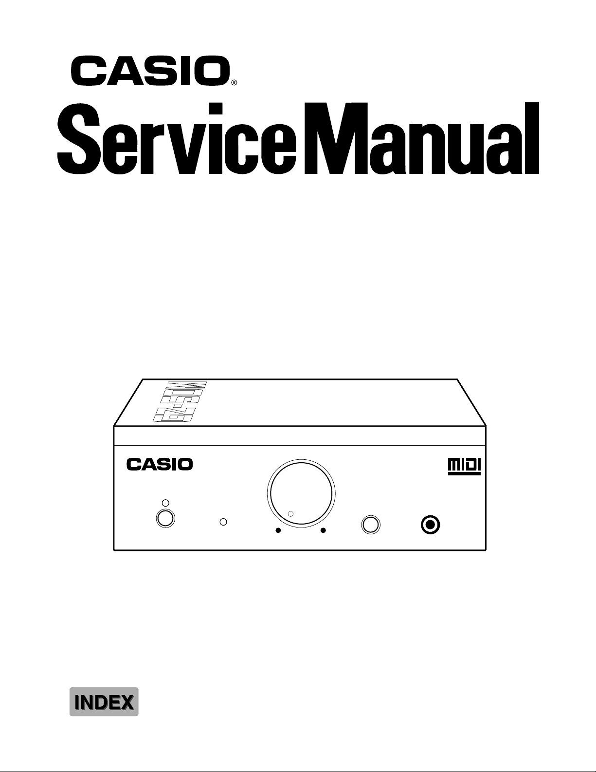
GZ-50M
(with price)
POWER
VOLUME
MIDI
MONITOR
MIN
GM SOUND MODULE
GM SOUND MODULE
GENERAL
DEMO PHONES
MAX
Page 2

CONTENTS
Specifications . . . . . . . . . . . . . . . . . . . . . . . . . . . . . . . . . . . . . . . . . . 2
MIDI Messages receivable with GZ-50M . . . . . . . . . . . . . . . . . . . . . 3
Block Diagram . . . . . . . . . . . . . . . . . . . . . . . . . . . . . . . . . . . . . . . . . 9
Circuit Description . . . . . . . . . . . . . . . . . . . . . . . . . . . . . . . . . . . . . 10
Major waveforms . . . . . . . . . . . . . . . . . . . . . . . . . . . . . . . . . . . . . . 14
PCB View and Check Points . . . . . . . . . . . . . . . . . . . . . . . . . . . . . . 16
Schematic Diagram . . . . . . . . . . . . . . . . . . . . . . . . . . . . . . . . . . . . 17
Exploded View . . . . . . . . . . . . . . . . . . . . . . . . . . . . . . . . . . . . . . . . 18
Parts List . . . . . . . . . . . . . . . . . . . . . . . . . . . . . . . . . . . . . . . . . . . . 19
SPECIFICATIONS
GENERAL
Sound source: The General MIDI system 1
Number of tones: 128
Number of drum sets: 8
Number of layer voice: 32
Digital effects: 10, including Reverb-1, Reverb-2, Reverb-3, Chorus, Tremolo,
Phase Shifter, Organ SP, Enhancer, Flanger, EQ Loudness
Demonstration tune: Suite for Rebecca (Arranged and programmed by Wojtek Gogoleski)
Volume control: Analog volume
MIDI monitor: LED
Tuning: Center: 440 Hz
Terminals: Headphone Jack [Output impedance: 68 Ω, Output voltage: 0.3 V(rms)MAX],
Line Out Jack [Output impedance: 2 KΩ, Output voltage: 1.5 V8rms) MAX],
MIDI IN Jack, AC Adapter Jack (9 V)
Power source: AC source only: AC adapter
Power consumption: 2.8 W
Dimensions (HWD): 35 x 113 x 169 mm (1-3/8 x 4-7/16 x 6-5/8 inches)
Weight: 450 g (1 lbs)
ELECTRICAL
Current drain with 9 V DC:
No sound output 210 mA ± 20%
Maximum volume 230 mA ± 20%
with 32 polyphonic in tone No.078
Volume; maximum, Touch response: maximum
Phone output Level (Vrms with 8 Ω load each channel):
with keys C6 and F6 in tone No.078 85 mV ± 20%
Line output level (Vrms with 47 KΩ load each channel):
with keys C6 and F6 in tone No.078 300 mV ± 20%
Minimum operating voltage: 4.0 V
— 2 —
Page 3

MIDI messages receivable with GZ-50M
MIDI channel: 1 - 16 channel
Note On/Off: Note number 0 - 127
Velocity 1 - 127
Program change: 0 - 127 on channel 1 -9 & 11 - 16
0 - 7 on channel 10
Pitch bend: 00H/00H - 7FH/7FH
Control change: Modulation Control No. 1 0 - 127
Volume Control No. 7 0 - 127
Pan Control No. 10 0 (left) - 64 (center) - 127 (right)
Expression Control No. 11 0 - 127
Hold Control No. 64 0 - 63: Off, 64 - 127: On
Sostenuto Control No. 66 0 - 63: Off, 64 - 127: On
Soft Control No. 67 0 - 63: Off, 64 - 127: On
Effect depth Control No. 91 0 -127
All sounds off Control No. 120
Reset all controllers Control No. 121
* See next page for information about the initial settings.
Local control On/Off Control No. 122 0: Off, 127: On
All notes off Control No. 123
Registered Parameter Number (RPN) Control No. 36: LSB, No.37: MSB
Pitch bend sense Control No. 100 00H
Control No. 101 00H
Data entry Control No. 6 00H - 0CH
Control No. 36 00H
Fine tuning Control No. 100 01H
Control No. 101 00H (20H: -50 cents)
Data entry Control No. 6 20H - 40H - 60H (40H: center)
Control No. 36 00H (60H: +50 cents)
Coarse tuning Control No. 100 02H
Control No. 101 00H (34H: -12 seminotes)
Data entry Control No. 6 34H - 40H - 4CH (40H: center)
Control No. 36 00H (4CH: +12 seminotes)
RPN null Control No. 100 7FH
Control No. 101 7FH
Active sensing:
Channel pressure: Reconized as modulation
System exclusive: Effect change [F0][44][0B][09][xx][F7]
[xx]: [00] - [09], [0F]
[00]: Reverb1 (Stage)
[01]: Reverb2 (Hall)
[02]: Reverb3 (Room)
[03]: Chorus
[04]: Tremolo
[05]: Phase shifter
[06]: Organ speaker
[07]: Enhance
[08]: Flanger
[09]: EQ Loundness
[0F]: Effect OFF
GM system on [F0][7E][7F][09][01][F7]
* See next page for information about the initial settings in The General MIDI system.
— 3 —
Page 4

The initial setteings
Pitch bend: 0
Modulation: 0 (Off)
Expression: 127 (Maximum)
Sustain: 0 (Off)
Sostenuto: 0 (Off)
Soft: 0 (Off)
Channel pressure: 0 (Off)
RPN: Null
The initial settings in The General MIDI system
Channel 1 - 9 & 11 - 16
Program change: 000 (Piano)
Pitch bend: LSB: 40H, MSB: 00H
Modulation: 0 (Off)
Volume: 100
Pan: 64 (Center)
Expression: 127 (Maximum)
Sustain: 0 (Off)
Soft: 0 (Off)
Effect depth: 127 (Maximum)
Pitch bend sense: 02 (2 seminotes)
Coarse tune: LSB:40H, MSB:00H
Fine tune: LSB:40H, MSB:00H
RPN: Null
Channel pressure: 0 (Off)
Channel 10
Drum set No.: 0
Volume: 100
Pan: 64 (Center)
Expression: 127 (Maximum)
Effect depth: 127 (Maximum)
Soft: 0 (Off)
— 4 —
Page 5
Model GZ-50M MIDI Implementation Chart
Function ... Transmitted Recognized Remarks
Version: 1.0
Basic Default
Channel Changed
Default
Mode Messages
Altered
Note
Number: True voice
Velocity Note ON
Note OFF
After Key's
Touch Ch's
Pitch Bender
01
06, 38
Control 07
Change 10
11
64
66
67
91
100, 101
120
121
X
X
X
X
❊❊❊❊❊❊❊❊❊❊❊❊❊❊
X
❊❊❊❊❊❊❊❊❊❊❊❊❊❊
X
X
X
X
X
X
X
X
X
X
X
X
X
X
X
X
X
1-16 channel
1-16 channel
Mode 3
X
❊❊❊❊❊❊❊❊❊❊❊❊❊❊
0 ~ 127
12 ~ 108 *1
O
9nH v = 1~127
X
9nH v = 0, 8nH V=❊❊
X
O
*2
O
O
*2
O
*3
O
O
O
O
O
O
O
O
*3
O
O
*1:Different per tones.
❊❊ = No relation
Modulation
Data entry
Volume
Pan
Expression
Hold 1
Sostenuto
Soft
External effect depth
RPN LSB • MSB
All sounds off
Reset all controllers
Program
Change : True #
System Exclusive
System : Song Pos
Common : Song Sel
: Tune
System : Clock
Real Time : Commands
Aux : Local ON/OFF
Messages : All notes OFF
: Active Sense
: Reset
Remarks
Mode 1 : OMNI ON, POLY Mode 2 : OMNI ON, MONO
Mode 3 : OMNI OFF, POLY Mode 4 : OMNI OFF, MONO
X
❊❊❊❊❊❊❊❊❊❊❊❊❊❊
X
X
X
X
X
X
X
X
X
X
*2: Vibrato effect is obtained when received either message of modulation or channel
after touch.
*3: Reception of pitch bend sense, fine tune, coarse tune, and RPN Null.
*4: GM system on [F0][7E][7F][09][01][F7]
Effect Change [F0][44][0B][09][xx][F7]
O
❊❊❊❊❊❊❊❊❊❊❊❊❊❊
O
X
X
X
X
X
X
O
O
X
0 ~ 127
*4
[xx]: E_0[00] - E_9[09], Off[0F]
O
X
: No
: Yes
— 5 —
Page 6

LIST OF TONES AND OCTAVE RANGES
TONE NO./TONE NAME
PIANO
000 PIANO 032 WOOD BASS
001 HARD PIANO 033 ELEC BASS 1
002 STUDIO PIANO 034 ELEC BASS 2
003 HONKY-TONK 035 FRETLESS BASS
004 ELEC PIANO 1 036 SLAP BASS 1
005 ELEC PIANO 2 037 SLAP BASS 2
006 HARPSICHORD 038 SYNTH-BASS 1
007 CLAVELECTRO 039 SYNTH-BASS 2
GM OCT AVE RANGE
A0 – C8
A0 – C8
A0 – C8
A0 – C8
E1 – G7
E1 – G7
F2 – F6
C2 – C7
TONE NO./TONE NAME
BASS
CHROMATIC PERCUSSION STRING/ORCHESTRA
008 CELESTA 040 VIOLIN
009 GLOCKENSPIEL 041 VIOLA
010 MUSIC BOX 042 CELLO
011 VIBRAPHONE 043 CONTRABASS
012 MARIMBA 044 TREMOLO STR
013 XYLOPHONE 045 PIZZICATO STR
014 TUBULAR BELLS 046 HARP
015 DULCIMER 047 TIMPANI
C4 – C8
C5 – C8
C4 – C6
F3 – F6
C3 – C6
F4 – C7
C4 – F5
C4 – C6
GM OCT AVE RANGE
E1 – G3
E1 – G3
E1 – G3
E1 – G3
E1 – G3
E1 – G3
E1 – G3
E1 – G3
G3 – C7
C3 – C6
C2 – C5
E1 – G3
E1 – C7
E1 – C7
B0 – G7
C2 – A3
ORGAN ENSEMBLE
016 ELEC ORGAN 048 STRINGS 1
017 JAZZ ORGAN 049 STRINGS 2
018 ROCK ORGAN 050 SYNTH-STR 1
019 CHURCH ORGAN 051 SYNTH-STR 2
020 REED ORGAN 052 CHOIR
021 ACCORDION 053 MOON VOICE
022 HARMONICA 054 SYNTH-VOICE
023 BANDNEON 055 ORCHESTRA HIT
C2 – C7
C2 – C7
C2 – C7
A0 – C8
C2 – C7
F3 – F6
C4 – C6
F3 – F6
GUITAR BRASS
024 GUT GUITAR 056 TRUMPET
025 ACOUS GUITAR 057 TROMBONE
026 JAZZ GUITAR 058 TUBA
027 ELEC GUITAR 059 MUTE TRUMPET
028 MUTE GUITAR 060 FRENCH HORN
029 DIST GUITAR 1 061 BRASS
030 DIST GUITAR 2 062 SYNTH-BRASS 1
031 GT HARMONICS 063 SYNTH-BRASS 2
E2 – C6
E2 – C6
E2 – D6
E2 – D6
E2 – D6
E2 – D6
E2 – D6
E2 – D6
E1 – C7
E1 – C7
C2 – C7
C2 – C7
C3 – G5
C3 – G5
C3 – C6
C3 – C5
A#3 – A#6
A#1 – D#5
F1 – G3
A#3 – A#5
F2 – F5
C2 – C7
C2 – C7
C2 – C7
— 6 —
Page 7
TONE NO./TONE NAME
GM OCT AVE RANGE
TONE NO./TONE NAME
GM OCT AVE RANGE
REED SYNTH-SFX
064 SOPRANO SAX 096 PEARL DROP C2 – C7
065 ALTO SAX 097 SOUNDTRACK C2 – C7
066 TENOR SAX 098 CRYSTAL C2 – C7
067 BARITONE SAX 099 ATMOSPHERE C2 – C7
068 OBOE 100 BRIGHTNESS C2 – C7
069 ENGLISH HORN 101 LABYRINTH C2 – C7
070 BASSOON 102 ECHOES C2 – C7
071 CLARINET 103 COSMIC SOUND C2 – C7
F#3 – D#6
C#3 – G#5
F#2 – D#5
C#2 – G#4
A#3 – G6
E3 – A5
A#1 – C5
D3 – G6
PIPE ETHNIC
072 PICCOLO 104 SITAR C3 – F5
073 FLUTE 105 BANJO C3 – C6
074 RECORDER 106 SHAMISEN D3 – G5
075 PAN FLUTE 107 KOTO G3 – C6
076 BOTTLE BLOW 108 THUMB PIANO C3 – G5
077 SHAKUHACHI 109 BAG PIPE C2 – F5
078 WHISTLE 110 FIDDLE G3 – C7
079 OCARINA 111 SHANAI C3 – C5
D5 – C8
C4 – C7
C4 – C7
C4 – C7
C4 – C7
G3 – C6
C4 – C7
C4 – C6
SYNTH-LEAD
080 SYNTH - LEAD 1 112 BELLS C5 – C6
081 SYNTH - LEAD 2 113 AGOGO C4 – C5
082 CALLIOPE 114 STEEL DRUM E3 – E5
083 POWER LEAD 115 WOOD BLOCK C4 – C5
084 METAL LEAD 116 TAIKO C4 – C5
085 ANGEL CHOIR 117 TOM C4 – C5
086 FIFTH LEAD 118 ELEC TOM C4 – C5
087 BASS+LEAD 119 REVERSE CYMBAL C4 – C5
A0 – C8
A0 – C8
C2 – C7
C2 – C7
C2 – C7
C2 – C7
C2 – C7
A0 – C8
PERCUSSION
*1
*1
*1
*1
*1
SYNTH-PAD SFX
*1
*1
*1
*1
*1
*1
*1
C4 – C5
C4 – C5
C4 – C5
C4 – C5
C4 – C5
C4 – C5
C4 – C5
C4 – C5
088 FANTASY
089 WARM STRINGS
090 SYNTH-ENS
091 SPACE CHORUS
092 GLASS HARMONICA
093 ILLUSION
094 COUNTRY FARM
095 SYNTH-PAD
C2 – C7
C2 – C7
C2 – C7
C2 – C7
C2 – C7
C2 – C7
C2 – C7
C2 – C7
120 GT FRET NOISE
121 BREATH NOISE
122 SEASHORE
123 BIRD
*1
124 TELEPHONE
125 HELICOPTER
126 APPLAUSE
127 GUNSHOT
*1 Tone without scale.
— 7 —
Page 8

LIST OF DRUM SOUNDS
NOTE NO. DRUM INSTRUMENT NAME
B1
C2
D2
E2
F2
G2
A2
B2
C3
D3
E3
F3
G3
A3
B3
C4
D4
E4
F4
G4
A4
B4
C5
D5
E5
F5
G5
A5
B5
C6
C#2 37
D#2 39
F#2 42
G#2 44
A#2 46
C#3 49
D#3
F#3 54
G#3 56
A#3 58
C#4 61
D#4 63
F#4 66
G#4 68
A#4 70
C#5 73
D#5 75
F#5 78
G#5 80
A#5 82
35
36
38
40
41
43
45
47
48
50
51
52
53
55
57
59
60
62
64
65
67
69
71
72
74
76
77
79
81
83
84
Acoustic Bass Drum
Bass Drum 1
Side Stick
Acoustic Snare
Hand Clap
Electric Snare
Low Floor Tom
Closed Hi Hat
High Floor Tom
Pedal Hi Hat
Low Tom
Open Hi Hat
Low Mid Tom
High Mid Tom
Crash Cymbal 1
High Tom
Ride Cymbal 1
Chinese Cymbal
Ride Bell
Tambourine
Splash Cymbal
Cowbell
Crash Cymbal 2
Vibraslap
Ride Cymbal 2
High Bongo
Low Bongo
Mute High Conga
Open High Conga
Low Conga
High Timbale
Low Timbale
High Agogo
Low Agogo
Cabasa
Maracas
Short Whistle
Long Whistle
Short Guiro
Long Guiro
Claves
High Wood Block
Low Wood Block
Mute Cuica
Open Cuica
Mute Triangle
Open Triangle
Shaker
Suzu
Sticks
— 8 —
Page 9

BLOCK DIAGRAM
MIDI IN
Effect RAM
(256K-bit)
LSI102
LC33832M-70
Photocoupler
IC106
PC900VP
Power ON signal
EA0 ~ EA14
ED0 ~ ED7
CPU
LSI104
HD6433298A42F
A0 ~
A14
D0~D7
A0 ~ A14
DSP
LSI103
HG51B115FD
A0 ~ A3
RESET
POWER
Working Storage RAM
(64K-bit)
LSI106
SRM2264LM90-B
RA0 ~ RA19
RD0 ~ RD15
Sound Source ROM
TC5316200CF-C117
Reset IC
IC104
RH5VL36A
Power Switch
(16M-bit)
LSI105
DC IN
VCC
Power Supply Circuit
DVDD
AVDD
D102, D103
Q101~Q105
Line Out
VDD
Mute Circuit
Q108, Q109
WCK1 SLOP BCK
D/A Converter
LSI101
UPD6376GS
Filter
IC103
Main
Volume
Line Out Amplifier
M5218AFP
Filter
IC103
IC102
Headphone
Amplifier
IC101
LA4525
Headphone
— 9 —
Page 10

CIRCUIT DESCRIPTION
CPU (LSI104: HD6433298A42F)
The 16-bit CPU contains a 32k-bit ROM, a 1k-bit RAM, seven 8-bit I/O ports and MIDI interfaces. The
CPU receives MIDI message and interprets it using the working storage RAM. For instance, when receiving NOTE ON message, the CPU sends the note number and its velocity to the DSP in order to produce
sound of that note.
The following table shows the pin functions of LSI104.
Pin No. Terminal In/Out Function
1 P50/TXD — Not used
2 P51/RXD In MIDI signal input
3 P52/SCK Out Reset signal output
4 -RESET In Reset signal input
5 -NMI In Power ON trigger signal input
6 VCC In +5V source
7 -STBY In Standby signal input. Connected to +5V.
8 VSS In Ground (0V) source
9, 10 XTAL, EXTAL In 20MHz clock input
11, 12 MD1, MD0 In Mode selection input
13 AVSS In Ground (0V) source
14 ~ 20 P70 ~ P76 In Not used. Connected to ground.
21 P77 In DEMO button input signal
22 AVCC In +5V source
23 P60 Out LED drive signal output
24 ~30 P61 ~ P67 — Not used
31 VCC In +5V source
32 P27 — Not used
33 ~ 48 A0 ~ A14 Out Address bus
40 VSS In Ground (0V) source
49 ~ 56 D0 ~ D7 In/Out Data bus
57, 58 P40, P41 — Not used.
59 P42 Out Power ON signal output
60 P43 Out Read enable signal output
61 P44 In Write enable signal output
62 P45 — Not used
63 P46 Out Terminal for 10 MHz clock check point
64 P47 — Not used. Connected to +5 V source.
DIGITAL SIGNAL PROCESSOR (LSI03: HG51B155FD-1)
Upon receipt of a note number and its velocity, the DSP reads sound and velocity data from the sound
source ROM in accordance with the received MIDI message. Then it provides 16-bit serial signal to the
DAC. If a control change message or "an effect change" of exclusive message has been received, the
DSP adds the effect to the sound data using the effect RAM.
The following table shows the pin functions of LSI103.
— 10 —
Page 11

Pin No. Terminal In/Out Function
1 ~ 8 CD0 ~ CD7 In/Out Data bus
9, 10 CE1, TRSB — Not used
11 GND7 In Ground (0V) source
12 CK16 Out Terminal for 24.576 MHz clock check point
13 VCC1 In +5V source
14 CK0 In Clock input. Connected to terminal CK16.
15 TCKB — Not used
16 VCC1 In +5V source
17 GND1 In Ground (0V) source
18, 19 XT0, XT1 In/Out 24.576 MHz clock input/output
20 SGL In System control terminal. Single chip system: Open
21 CCSB In Chip select signal input
22 ~ 25 CA0 ~ CA3 In Address bus
26 CE0 In Not used. Connected to ground.
27 CWRB In Write enable signal
28 CRDB In Read enable signal
29 ~ 32 — — Not used
33 RESB In Reset signal input
34 TESB In Not used. Connected to +5V.
35 ~ 39 — — Not used
40 ~ 49
52 ~ 57
RD0 ~ RD15 In Data bus for the sound source ROM
50 VCC2 In +5V source
51 GND2 In Ground (0V) source
58 RA23 Out Not used
59 RA22 Out Chip select signal for the sound source ROM
60, 61 RA20, RA21 Out Not used
62 ~ 73
75 ~ 82
RA0 ~ RA19 Out Address bus for the sound source ROM
74 GND5 In Ground (0V) source
83 WOK2 Out Not used
84 VCC3 In +5V source
85 GND3 In Ground (0V) source
86 WOK1 Out Word clock for the DAC
87 SOLM Out Not used
88 SOLP Out Serial sound data output
89 BOK Out Bit clock output
90 ~ 92 — — Not used
93 VCC5 In +5V source
94, 95
97 ~ 105
107,109
EA0 ~ EA12 Out Address bus for the effect RAM
110, 112
96 EWEB Out Write enable signal for the effect RAM
— 11 —
Page 12

Pin No. Terminal In/Out Function
106 EOEB Out Read enable signal output for the effect RAM
108 VCC7 In +5V source
111 ECEB Out Chip select signal output for the effect RAM
113 ~ 117 ED11 ~ ED15 — Not used
118 VCC4 In +5V source
119 GND4 In Ground (0V) source
120 ~ 122 ED8 ~ ED10 — Not sued
123 ~ 130 ED0 ~ ED7 In/Out Data bus for the effect RAM
131 GND5 In Ground (0V) source
132 ~ 134 — — Not used. Connected to ground.
135, 136 — — Not used
Block diagram of DSP and DAC circuit
Sound Source ROM
LSI105
TC5316200CF-C117
CE
A0 ~ A19 D0 ~ D15
RA22
RA0 ~
RA19
RD0 ~
RD15
SOLP: Sound data
BOK: Bit clock
WOK1: Word clock
DAC
A13
RD
D0 ~ D7
A0 ~ A3
CCSB
CRDB
DSP
LSI103
HG51B155FD-1
SOLP
BOK
WOK1
LSI101
SI
CLK
LRCK
UPD6376GS
ROUT
LOUT
Power ON signal
WR
RESET
CWRB
RESB
ECEB EOEB
OE
CS
WE
EWEB
ED0 ~
ED15
D0 ~ D15
EA0 ~
EA14
A0 ~ A14
PG
X102
24.576 MHz
Effect RAM (256K-bit)
LSI102
LC33832M-70
DAC (LSI101: UPD6376GS)
The DAC receives 16-bit serial data and two clocks output from the DSP. The DAC converts the data into
analog waveforms by each channel and output them separately.
The following table shows the pin functions of LSI101.
— 12 —
Page 13

Pin No. Terminal In/Out Function
1 SEL In Mode selection terminal. Connected to ground.
2 D.GND In Ground (0V) source for the internal digital circuit
3 NC Not used.
4 DVDD In +5V source for the internal digital circuit
5 A.GND In Ground (0V) source for the right channel
6 R.OUT Out Right channel sound waveform output
7, 8 A.VDD In +5V source for the internal analog circuit
9 R.REF In Right channel reference voltage terminal
10 L.REF In Left channel reference voltage terminal
11 L.OUT Out Left channel sound waveform output
12 A.GND In Ground (0V) source for the left channel
13 LRCK In Word clock input
14 LRSEL In Not used. Connected to ground.
15 SI In Sound data input
16 CLK In Bit clock input
POWER SUPPLY CIRCUIT
The power supply circuit generates five voltages as shown in the following table. VDD voltage is always
generated. The others are controlled by the power ON signal output from the CPU.
Name Voltage For operation of
VDD +5 V CPU, Reset IC, Working strage RAM
DVDD +5 V DSP, Effect RAM, DAC, Pilot lamp
AVDD +5V DAC, Filter
AVCC +7 V Headphone amplifier, Line ount amplifier
VCC +8 V Mute circuit
RESET CIRCUIT
When an AC adapter is connected, the reset IC provides a low pulse to the CPU. The CPU then initializes
its internal circuit and clears the working storage RAM.
When the power switch is pressed, the CPU receives a low pulse of POWER signal. The CPU provides
the power ON signal to the power supply circuit and raises RESET signal to +5V to reset the DSP.
VDD
RESET
Reset IC
IC104
RH5VL36A
POWER
From power switch
VDD
CPU
LSI104
HD6433298A42F
-NMI
HG51B155FD-1
-RESET
Power ON signal
P42
To power supply circuit
DVDD VDD
DSP
LSI103
Working Storage RAM
LC3564SM-85
LSI106
— 13 —
Page 14

MAJOR WAVEFORMS
1
2
CH1: CH2:
1
Voltage VDD
Emitter of Q105
2
Initial reset signal
RH5VL36A pin 1
0.1 s
CH1
3
0.1 s
CH1
CH2
4
CH2
5
5 V5 V
CH1: CH2:
3
Power ON trigger -NMI
HD6433298A42F pin 5
4
Power ON signal
HD6433298A42F pin 59
5
Reset signal
HD6433298A42F pin 3
5 V5 V
6
7
8
5 VCH1: 5 VCH2: 5 VCH3: 5 VCH1:
6
Word clock WOK1
UPD6376GS pin 13
7
Data SI (Note OFF)
UPD6376GS pin 15
8
Bit clock BOK
UPD6376GS pin 16
5 µs
CH1
CH2
CH3
9
9 MIDI data
PC900VP pin 4
Basic channel
Note No.
Velocity
2 ms
CH1
: 1
: 60 (C3)
: 127 (Maximum)
— 14 —
Page 15

0
A
1 ms
CH1
CH2
B
C
1 ms
CH1
CH2
D
E
50 mV
~
CH1: CH2:
0
DAC output
UPD6376GS pin 11
A
Filter output
M5218AFP pin 1
50 mV
~
CH1: CH2:50 mV
B
~
.5 V
~
Line out amp. input (L-ch)
C111
C
Line out amp. output (L-ch)
C161
1 ms
CH1
CH2
Program change (Tone No)
Note No. (Key)
Velocity
: 81 (A4)
: 127 (Maximum)
: 078 (Whistle)
CH1: CH2:10 mV
D
Headphone amp. input
~
LA4525 pin 7
E
Headphone amp. output
LA4525 pin 1
1 V
~
— 15 —
Page 16

PCB VIEW AND CHECK POINTS
2
13
3
4
5
1
R112
C152
LSI104
LSI106
C105
C108
C109
C186
J101
D104
X101
R150
R109
B
D102
C114
C183C185
L104
C161
Q103
C119
R149
1
C184
J102
R171
E
CA101
C187
R145
C140
C118
R185
Q108
C117
R119
R173
C110
C121
D105
IC104
R144
C138
R158
R159
5
X102
C116
FB112
R117
R160
Q105
C104
R118
C112
C160
C107
J103
R170
C120
C113
C156
R175
Q109
C111
C106
IC101
D106
D107
C163
C157
C125
1
R181R182
R184
C137
CB101
D109
LSI101
3
IC106
Q110R176
C164
C131
C130
R130
C103
C102
C122
FB111
C162
LSI103
C101
J104
R134
C136
C135
IC103
C123
R177
R178
C188
C182
C153
C133
9
8
7
6
10
11
Top View
— 16 —
VR101
151214
Page 17
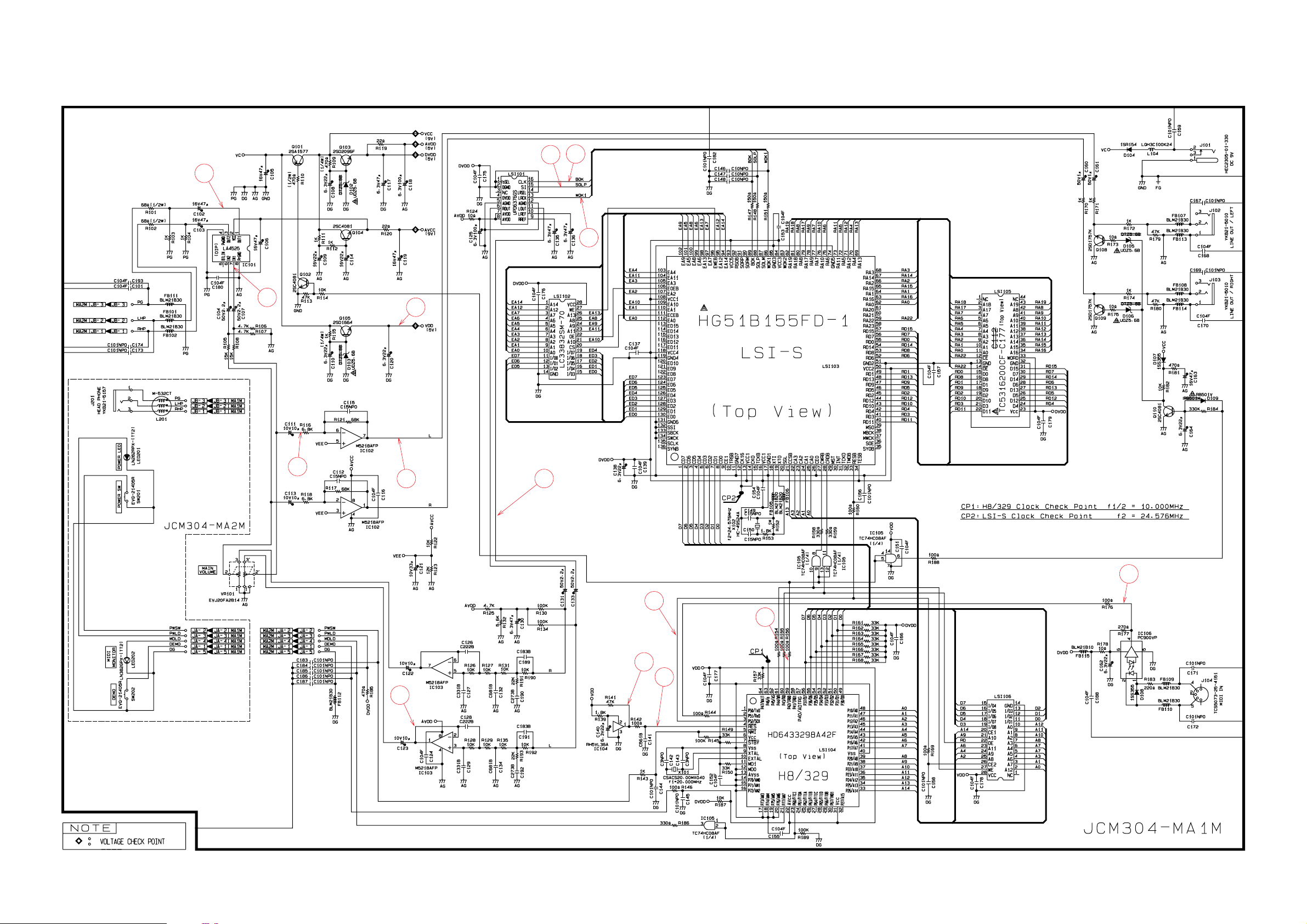
PCBs JCM304-MA1M/MA2M
SCHEMATIC DIAGRAM
15
8.4
14
0.0
7.3
8.0
0.7
5.6
7.8
5.6
5.0
5.0
7.2
8
7
6
1
12
11
13
10
9
5
4
2
3
SRM2264LM90
— 17 —
Page 18

EXPLODED VIEW
6
3
1
4
5
2
— 18 —
Page 19

PARTS LIST
GZ-50M
Notes: 1. Prices and specifications are subject to change with-
out prior notice.
2. As for spare parts order and supply, refer to the
"GUIDEBOOK for Spare parts Supply", published
seperately.
3. The numbers in item column correspond to the same
numbers in drawing.
Page 20

FOB Japan
N Item Code No. Parts Name Specification Q N.R.Yen R
Unit Price
Main PCB M304-MA1M
N 1 6923 7150 PCB ass'y M304-MA1M with M140210*1
1
7,880 A
M304-MA2M
N LSI101 2114 4221 LSI UPD6376GS-E1 1 200 A
N LSI102 2012 0777 LSI LC33832M-70-TLM 1 410 A
N LSI103 2012 1316 LSI HG51B155FD-1 1 1,160 A
N LSI104 2012 0462 LSI HD6433298A42F 1 860 A
N LSI105 2012 1498 LSI TC5316200CF-C117 1 990 A
N LSI106 2012 0770 LSI SRM2264LM90-B 1 280 A
IC101 2114 2632 IC LA4525 1 89 A
N IC102, IC103 2114 4214 IC M5218AFP-600C 2 39 A
N IC104 2105 4536 IC RH5VL36AA-T1 1 44 A
N IC105 2105 4445 IC HD74HC08FPTR 1 34 A
N IC106 2114 4326 IC, Photocoupler PC900VP 1 140 A
N Q101
2250 1176 Chip transistor 2SA1577T106R
N Q102, Q104, 2252 1169 Chip transistor 2SC4081-T106S
1
3
13 B
8B
Q110
N
Q103 2250 1183 Transistor 2SD2096T114F
160B
N Q105 2253 0644 Transistor 2SD1664T101R 1 23 B
N Q108, Q109
2253 0651 Chip transistor 2SD1757KT146S
N D102, D103, 2360 2541 Chip zener diode DTZTT115.6B
2
4
18 B
15 B
D105, D106
N D104 2390 2058 Chip diode 1SR154-400TE25 1 20 C
N D107, D108 2390 1820 Chip diode 1SS355TE-17 2 9 C
N D109 2390 2310 Chip schottky diode RB501H-TT11 1 22 B
J101 3501 7049 Power jack HEC2305-01-330 1 29 A
J102, J103 3612 0789 Jack YKB21-5010 2 60 A
N J104
3501 9786 DIN jack TCS5073-25-4151
1
130 B
N VR101 2765 1778 Volume, with nut EVJC20F03B14 1 110 A
N X101 2590 2100 Ceramic oscillator CSACS20.00MX040-TC 1 71 B
N X102 2590 2107 Crystal oscillator HC-49S24A 1 130 B
Sub PCB M304-MA2M
N J201 3501 9793 Phone jack YKB21-5157 1 57 A
LED201 2370 0686 LED LN282RPX-(TT2) 1 22 C
LED202 2370 0889 LED LN382GPX-(TT2) 1 26 C
SW201, SW202 3412 0903 Tact switch EVQ-21405R 2 15 B
Cabinet
N
2 6923 7480 Lower case M240162-1 1
N 3 6923 7440 Upper case M240161-1
N
4 6923 7450 Rotary knob M340189-1 1
N 5 6923 7460 Front panel M240160-1
N
6 6923 7470 Button M311687-7 2
1
1
210 C
570 C
21 C
110 C
11 C
Notes: N – New parts
M – Minimum order/supply quantity
R – Rank
— 19 —
Page 21

MA0700951A
 Loading...