Page 1
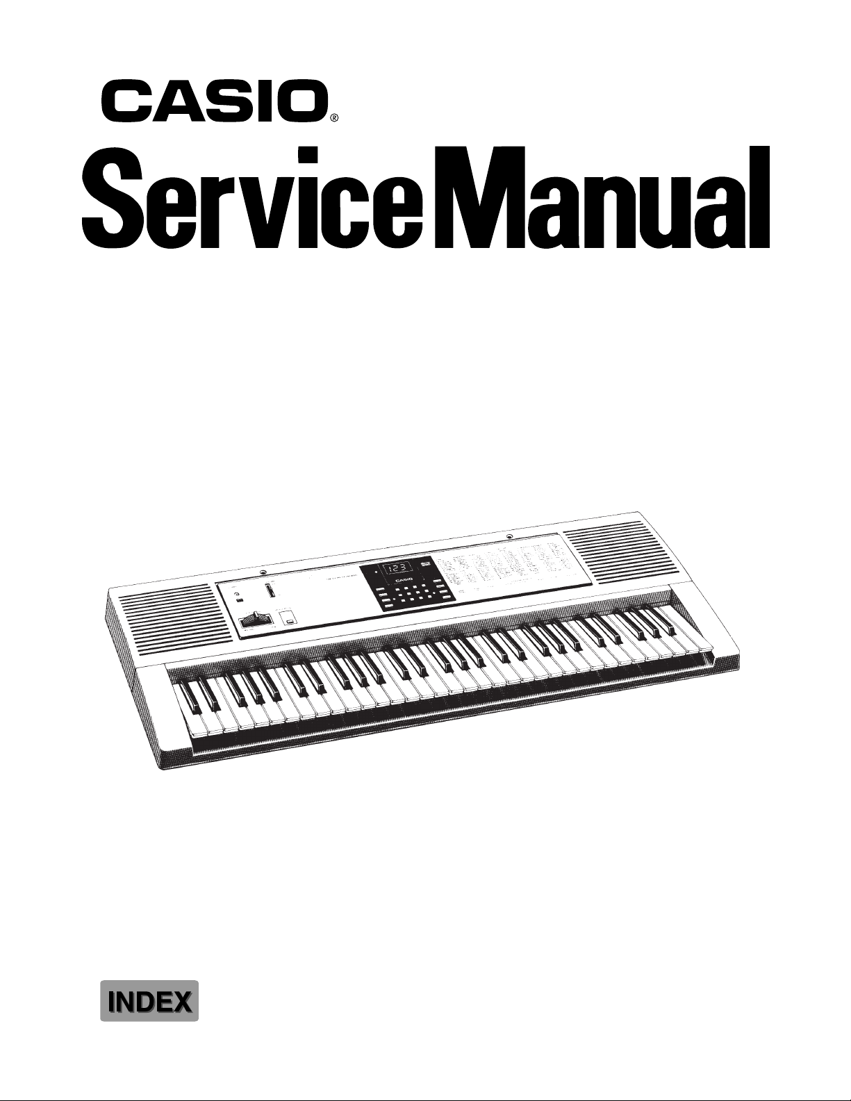
GZ-500
(with price)
GM SOUND KEYBOARD
GZ-500
Page 2

CONTENTS
Specifications . . . . . . . . . . . . . . . . . . . . . . . . . . . . . . . . . . . . . . . . . . 2
Operation . . . . . . . . . . . . . . . . . . . . . . . . . . . . . . . . . . . . . . . . . . . 3
Block Diagram . . . . . . . . . . . . . . . . . . . . . . . . . . . . . . . . . . . . . . . . . 8
Circuit Description . . . . . . . . . . . . . . . . . . . . . . . . . . . . . . . . . . . . . 9
Major waveforms . . . . . . . . . . . . . . . . . . . . . . . . . . . . . . . . . . . . . . 17
Schematic Diagrams . . . . . . . . . . . . . . . . . . . . . . . . . . . . . . . . . . . . 18
Exploded View . . . . . . . . . . . . . . . . . . . . . . . . . . . . . . . . . . . . . . . . 22
Parts List . . . . . . . . . . . . . . . . . . . . . . . . . . . . . . . . . . . . . . . . . . . . 23
SPECIFICATIONS
GENERAL
Number of keys: 61
Polyphonic: 32-note
Preset tones: 128, Drum set: 8
Keyboard controls: Touch response: On/Off
Digital effects: 10, including Reverb-1, Reverb-2, Reverb-3, Chorus, Tremolo,
Phase Shifter, Organ SP, Enhancer, Flanger, EQ Loudness
Modulation: On/Off, Depth setting range: 0 - 127
Pitch bend wheel: Bend sense: 0 - 12
Tuning control: 440Hz ± 50 cents
Built-in speakers: 12 cm dia. 2 W input rating: 2 pcs.
Terminals: Phone Jack [Output impedance: 100 Ω, Output voltage: 4.5 V(rms) MAX],
MIDI Jacks (IN, OUT), Assignable Jack, AC Adapter Jack (9 V)
Auto power off: Approximately 6 minutes after the last operation
Power source: 2-way AC or DC source
AC: AC adapter
DC: 6 D size dry batteries
Power consumption: 7.7 W
Dimensions (HWD): 129 x 942 x 367 mm (5-1/16 x 37-1/16 x 14-1/2 inches)
Weight: 5.3 kg (11.7 lbs) excluding batteries
ELECTRICAL
Current drain with 9 V DC:
No sound output 294 mA ± 20%
Maximum volume 940 mA ± 20%
with 32 polyphonic notes in tone No. 078
Volume; maximum, Velocity: maximum
Phone output level (Vrms with 8 load each channel):
with key A5 pressed in tone No. 078 100 mV ± 20%
Line output level (Vrms with 47 k load each channel):
with key A5 pressed in tone No. 078 1350 mV ± 20%
Minimum operating voltage: 6.0 V
— 2 —
Page 3
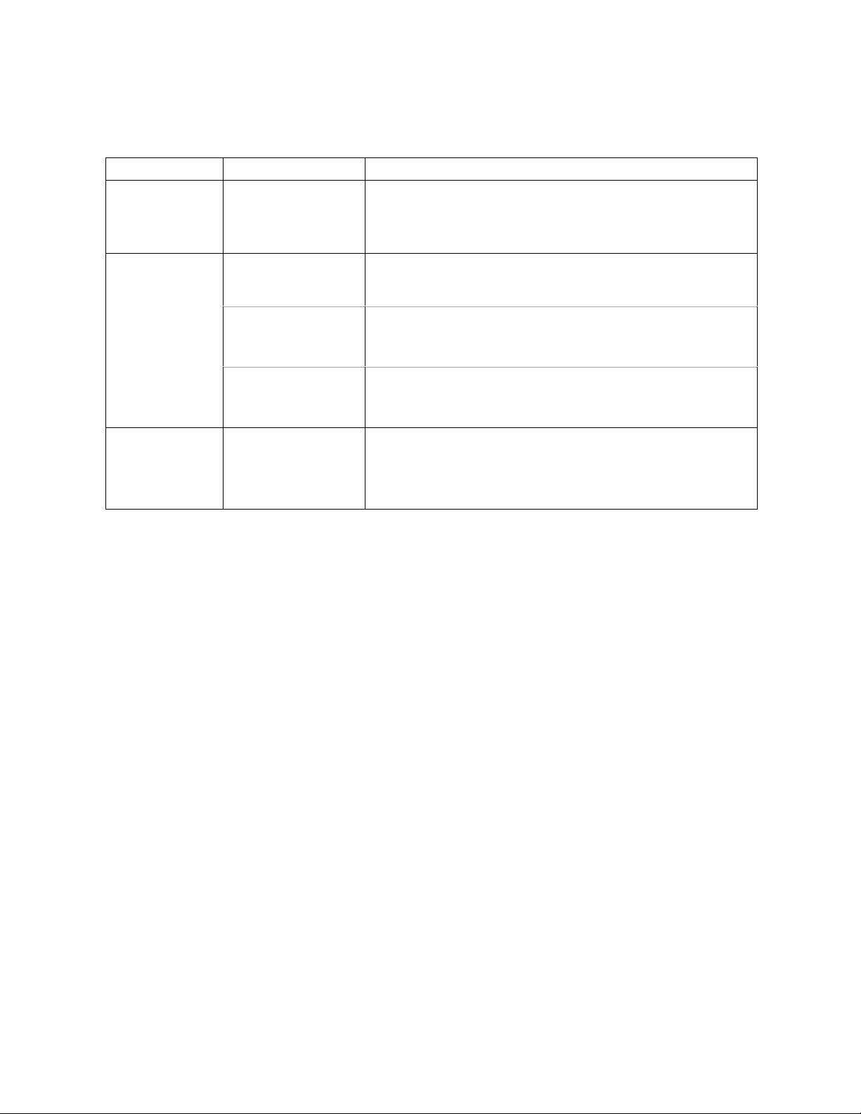
SETTING UP THE KEYBOARD
g
OPERATION
Item Settin
System Reset 1* 1. Press the control button and repeat it until the display
shows "Srt".
"SUr" and "Srt" will appear alternately on the display.
2. Press the + key.
Assignable Jack Sustain pedal 1. Press the control button and repeat it until the display
shows "JAC".
2. Using the +/- key, select "SUS" on the dispaly.
Sostenuto pedal 1. Press the control button and repeat it until the display
shows "JAC".
2. Using the +/- key, select "SoS" on the dispaly.
Soft pedal 1. Press the control button and repeat it until the display
shows "JAC".
2. Using the +/- key, select "SFt" on the dispaly.
GM Reset 3* 2* 1. Press the MIDI button and repeat it until the display shows
"Grt".
"SUr" and "Grt" will appear alternately on the display.
2. Press the + key.
3. Press the + key again.
Notes: 1* See the initial settings list as shown below.
2* See the initial settings in The General MIDI system on next page.
3* The exclusive message of "GM system on" will be tramsmitted when completing the operation.
System exclusive: GM system on [F0][7E][7F][09][01][F7]
Setting operation
The initial settings
Tone: 000 (Piano) Channel 1 - 9 & 11 - 16
dr0 (Drum set 0) Channel 10
Modulation: 0 (Off)
MIDI control change
Volume: 100
Pan: 64 (Center)
Expression: 127 (Maximum)
Effect depth: 127 (Maximum)
Pitch bend sense: 2
Coarse tune: 0 (Center)
Fine tuning: 0 (Center)
Digital effect: E-0 (Digital effect 0)
MIDI channel: 01
Channel On/Off: On
Octave shift: 0
Modulation depth: 064
Touch response: r-0 (Touch curve 0)
Velocity at touch
response OFF: 100
Assignable jack: SUS (Sustain pedal)
Local control On/Off: On
— 3 —
Page 4
The initial settings in The General MIDI system
Channel 1 - 9 & 11 - 16 Channel 10
Program change: 000 (Piano) Drum set No.: 0
Pitch bend: LSB: 40H, MSB: 00H
Modulation: 0 (Off)
Volume: 100 Volume: 100
Pan: 64 (Center) Pan: 64 (Center)
Expression: 127 (Maximum) Expression: 127 (Maximum)
Sustain: 0 (Off)
Soft: 0 (Off) Soft: 0 (Off)
Effect depth: 127 (Maximum) Effect depth: 127 (Maximum)
Pitch bend sense: 02 (2 seminotes)
Coarse tune: LSB:40H, MSB:00H
Fine tune: LSB:40H, MSB:00H
RPN: Null
Channel pressure: 0 (Off)
TRANSMITTING MIDI MESSAGES
Operation 1
MIDI messages of note on/off, velocity and modulation are transmitted no matter which MIDI channel is
selected.
Note on/off message is transmitted when the corresponding key is pressed/released.
Use the Octave Shift Button, shift the octave range up or down so that GZ-500 is able to send note
numbers 17 to 108 but the keyboard has 61 keys only.
Velocity is also transmitted when a key is pressed. GZ-500 sends the velocity in accordance with the
strength of the pressed key and the selected touch curve (sensitivity).
Data of modulation is transmitted when the corresponding wheel is operated.
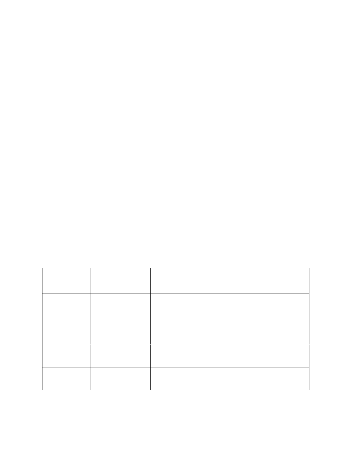
MIDI Message Setting Setting operation
Note On/Off Octave shift 1. Press the octave shift button.
2. Using the +/- key, select an octave range -2 to 1 you want.
Velocity Velocity curve 1. Press the control button and repeat it until the display
shows "tCH".
2. Using the 10-key, enter a number from 0 to 7.
Touch response OFF 1. Press the control button and repeat it until the display
shows "tCH".
2. Using the 10-key, enter a number 0.
3. Press the - key. The display will show "oFF".
Velocity at touch
response OFF
Modulation Modulation depth 1. Press the control button and repeat it until the display
1. Press the control button and repeat it until the display
shows "tCH".
2. Using the 10-key, enter a 3-digit number from 001 to 127.
shows "dEP".
2. Using the 10-key, enter a 3-digit number from 001 to 127.
— 4 —
Page 5
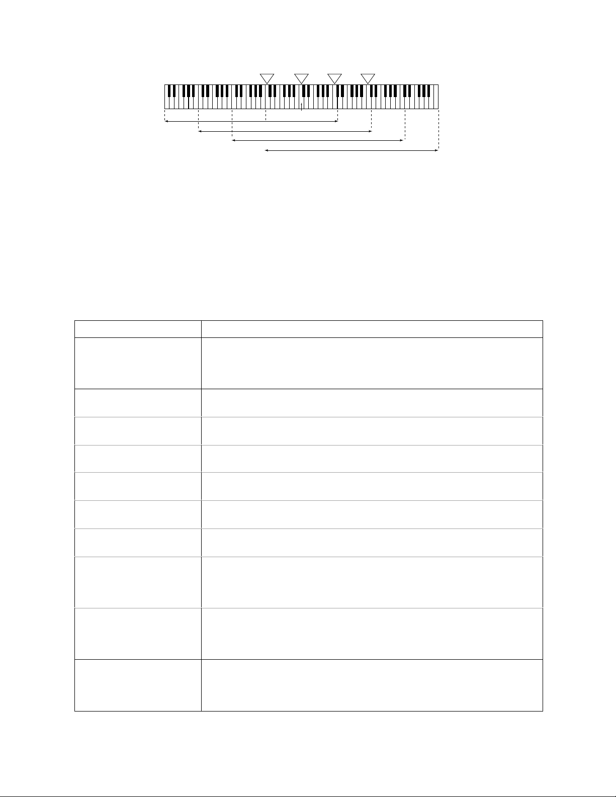
Octave shift setting and keyboard range
e
n
e
f
s
-21 0 -1
C4 (60)
Octave range when set to -2
Octave range when set to -1
Octave range when set to 0
Octave range when set to 1
Operation 2
The MIDI messages listed in the following table are transmitted when completing the setting operation.
The setting affects only on the currently selected MIDI channel. First select the desire MIDI channel
before changing settings.
Selecting a MIDI channel
1. Press the MIDI button.
The display shows the current MIDI channel, eg. "C01" means Channel 1.
2. Using the 10-key, enter a number from 1 to 16.
Changing Program Change / Control Change
MIDI Message Setting Operation
Program change 1. Reffering to the tone number list on the panel, find the 3-digit tone
number you desire.
2. Press the tone button.
3. Using the 10-key, enter the 3-digit number.
Control change
Volum
1. Press the MIDI button and repeat it until "voL" appears on the display.
2. Using the 10-key, enter a 3-digit number from 000 to 127.
1. Press the MIDI button and repeat it until "PAn" appears on the display.
Pa
2. Using the 10-key, enter a 3-digit number from 000 to 127.
Expression 1. Press the MIDI button and repeat it until "EPS" appears on the display.
2. Using the 10-key, enter a 3-digit number from 000 to 127.
Effect depth 1. Press the MIDI button and repeat it until "EFt" appears on the display.
2. Using the 10-key, enter a 3-digit number from 000 to 127.
Fine tun
1. Press the MIDI button and repeat it until "tUn" appears on the display.
2. Using the 10-key and the - key, enter a 2-digit number from -50 to 50.
Transpose 1. Press the MIDI button and repeat it until "trn" appears on the display.
2. Using the 10-key and the - key, enter a 2-digit number from -12 to 12.
All notes of
1. Press the MIDI button and repeat it until "Ano" appears on the display.
"SUr" and "Ano" will appear alternately on the display.
2. Press the + key.
3. Press the + key again to transmit the message.
All sounds off 1. Press the MIDI button and repeat it until "ASo" appears on the display.
"SUr" and "ASo" will appear alternately on the display.
2. Press the + key.
3. Press the + key again to transmit the message.
Reset all controller
1. Press the MIDI button and repeat it until "rAC" appears on the display.
"SUr" and "rAC" will appear alternately on the display.
2. Press the + key.
3. Press the + key again to transmit the message.
— 5 —
Page 6

The initial settings of MIDI control change
Pitch bend: +/- 0 (Center)
Modulation: 0 (Off)
Expression: 127 (Maximum)
Sustain: 0 (Off)
Sostenuto: 0 (Off)
Soft: 0 (Off)
Channel pressure: 0 (Off)
RPN: null
Operation 3
Messages of Digital Effect Type, which are system exclusive messages, are transmitted when completing
the following operation.
Transmitting a digital effect type
1. Press the tone button.
2. Press the digital effect button once when the digital effect indicator is off.
Press the digital effect button twice when the digital effect indicator is lighting up.
3. Using the 10-key, enter a number from 0 to 9.
4. The display shows the degital efffect type entered, eg. "E_3" means digital effect 3 (Chorus)
5. Wait for about a few seconds unitl the display show the tone number at Step 1.
System exclusive: Effect change [F0][44][0B][09][xx][F7]
[xx]: [00] - [09], [0F]
[00]: Reverb1 (Stage)
[01]: Reverb2 (Hall)
[02]: Reverb3 (Room)
[03]: Chorus
[04]: Tremolo
[05]: Phase shifter
[06]: Organ speaker
[07]: Enhance
[08]: Flanger
[09]: EQ Loundness
[0F]: Effect OFF
RECEIVING MIDI MESSAGES
The MIDI monitor blinks during receiving a MIDI message.
To recognize Note On/Off messages, set a MIDI channel on.
Setting on/off of a MIDI channel
1. Press the MIDI channel button.
2. Press the channel on/off button.
The LED lights when the MIDI channel is on.
The LED goes out when the MIDI channel is off.
Active sensing
This message checks if the MIDI cable is disconnected.
Once GZ-500 has received this message, it always counts time of an interval to a next MIDI message.
In case when GZ-5 receives no MIDI message for 420 msec of time, it will stop sound output and reset all
controllers, then it will cancel the function of active sensing.
— 6 —
Page 7

Transmittable Messages
Note No.: 12 ~ 72 (Oct. shift -2), 24 ~ 84 (Oct. shift -1)
36 ~ 96 (Oct. shift 0), 48 ~ 108 (Oct. shift 1)
Velocity: 1 ~ 127
Note Off: velocity 0
Program Change: 0 ~ 127 (Channels 1 - 9 & 11 - 16), 0 ~ 7 (Channel 10)
Pitch Bend: 00H / 00H ~ 7FH / 7FH
Control Change: Modulation 0 ~ 127
Volume 0 ~ 127
Pan 0 ~ 127
Expression 0 ~ 127
Sustain 0: Off, 127: On
Sosutenuto 0: Off, 127: On
Soft 0: Off, 127: On
Effect Depth 0 ~ 127
Pitch Bend Sense 00H / --H ~ 0CH / --H (12 seminotes)
Coarse Tune 34H / --H ~ 40H / --H ~ 4CH / --H
(-12 seminotes) ~ (center) ~ (+12 seminotes)
Fine Tune 20H / 00H ~ 40H / 00H ~ 60H / 00H
(-50 cents) ~ (center) ~ (+50 cents)
All Notes Off
All Sounds Off
Reset All Controllers
Exclusive: Effect Change
General MIDI On
Receivable Messages
Note No.: 0 ~ 127
Velocity: 1 ~ 127
Note Off: velocity 0
Program Change: 0 ~ 127(Channels 1 - 9 & 11 - 16), 0 ~ 7 (Channel 10)
Pitch Bend: 00H / 00H ~ 7FH / 7FH
Control Change: Modulation 0 (0 cent) ~ 127 (+/-50 cents)
Volume 0 ~ 127
Pan 0 (Left) ~ 64 (Center) ~ 127 (Right)
Expression 0 ~ 127
Sustain 0 ~ 63: Off, 64 ~ 127: On
Sosutenuto 0 ~ 63: Off, 64 ~ 127: On
Soft 0 ~ 63: Off, 64 ~ 127: On
Effect Depth 0 ~ 127
Pitch Bend Sense 00H / --H ~ 0CH / --H (12 seminotes)
Coarse Tune 34H / 00H ~ 40H / 00H ~ 4CH / 00H
(-12 seminotes) ~ (center) ~ (+12 seminotes)
Fine Tune 20H / 00H ~ 40H / 00H ~ 60H / 00H
(-50 cents) ~ (Center) ~ (+50 cents)
RPN Null
All Notes Off
All Sounds Off
Reset All Controllers
Channel Pressure: 0 (0 cent) ~ 127 (+/-50 cents)
Exclusive: Effect Change
General MIDI On
Active Sensing
— 7 —
Page 8
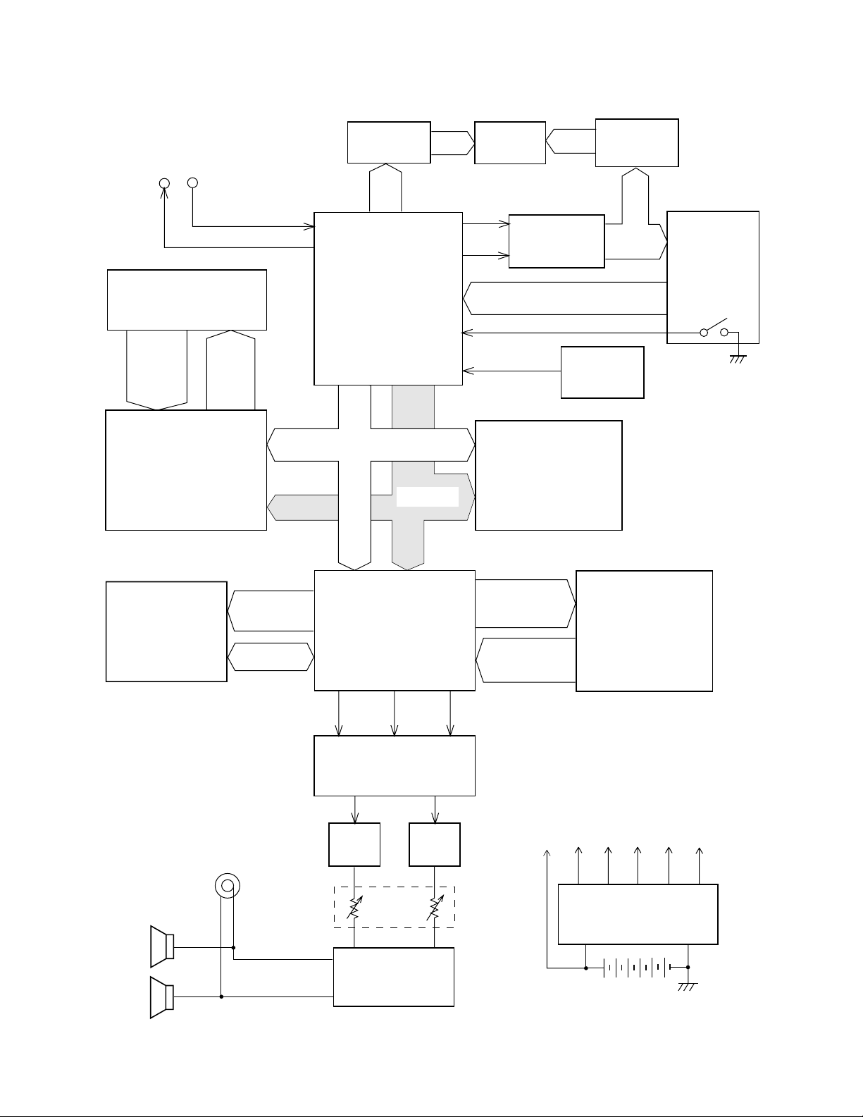
BLOCK DIAGRAM
MIDI
IN
OUT
Keyboard
FI0 ~ FI7
SI0 ~ SI7
Key Controller
LSI107
HG52E35P
KC0 ~
KC7
A0 ~ A2
LED driver
Q104 ~ Q111
LS0 ~
LS7
CPU
LSI106
HD6433298A42F
D0~D7
La ~ Lg, Lp
A0 ~
A14
A0 ~ A14
7-seg. LED
LEDs
P41
P40
KO Signal
Generator IC102
TC74HC174AF
KI1 ~ KI5
POWER
RESET
Working Storage RAM
SRM2264LM90-B
RH5VL36AA
(64K-bit)
LSI105
LED driver
KO0 ~
KO5
Reset IC
IC5
IC371
BA612
KO1 ~ KO3
Buttons
Power Switch
Effect RAM
(256K-bit)
LSI103
LC33832M-70
Speakers
EA0 ~ EA14
ED0 ~ ED7
Output
A0 ~ A3
DSP
LSI102
HG51B115FD
WCK1 SLOP BCK
D/A Converter
LSI104
UPD6376GS
Filter
IC101
Main
Volume
Power Amplifier
IC402
LA4598
Filter
IC101
RA0 ~ RA19
RD0 ~ RD15
VC
Sound Source ROM
(16M-bit)
LSI101
TC5316200CF-C112
LVDD
VCC
Power Supply Circuit
IC401, Q401 ~ Q405
AVDD
DVDD
VDD
— 8 —
Page 9

CIRCUIT DESCRIPTION
KEY MATRIX
KC0 KC1 KC2 KC3 KC4 KC5 KC6 KC7
FI0 C2 (1) C#2 (1) D2 (1) D#2 (1) E2 (1) F2 (1) F#2 (1) G2 (1)
SI0 C2 (2) C#2 (2) D2 (2) D#2 (2) E2 (2) F2 (2) F#2 (2) G2 (2)
FI1 G#2 (1) A2 (1) A#2 (1) B2 (1) C3 (1) C#3 (1) D3 (1) D#3 (1)
SI1 G#2 (2) A2 (2) A#2 (2) B2 (2) C3 (2) C#3 (2) D3 (2) D#3 (2)
FI2 E3 (1) F3 (1) F#3 (1) G3 (1) G#3 (1) A3 (1) A#3 (1) B3 (1)
SI2 E3 (2) F3 (2) F#3 (2) G3 (2) G#3 (2) A3 (2) A#3 (2) B3 (2)
FI3 C4 (1) C#4 (1) D4 (1) D#4 (1) E4 (1) F4 (1) F#4 (1) G4 (1)
SI3 C4 (2) C#4 (2) D4 (2) D#4 (2) E4 (2) F4 (2) F#4 (2) G4 (2)
FI4 G#4 (1) A4 (1) A#4 (1) B4 (1) C5 (1) C#5 (1) D5 (1) D#5 (1)
SI4 G#4 (2) A4 (2) A#4 (2) B4 (2) C5 (2) C#5 (2) D5 (2) D#5 (2)
FI5 E5 (1) F5 (1) F#5 (1) G5 (1) G#5 (1) A5 (1) A#5 (1) B5 (1)
SI5 E5 (2) F5 (2) F#5 (2) G5 (2) G#5 (2) A5 (2) A#5 (2) B5 (2)
FI6 C6 (1) C#6 (1) D6 (1) D#6 (1) E6 (1) F6 (1) F#6 (1) G6 (1)
SI6 C6 (2) C#6 (2) D6 (2) D#6 (2) E6 (2) F6 (2) F#6 (2) G6 (2)
FI7 G#6 (1) A6 (1) A#6 (1) B6 (1) C7 (1)
SI7 G#6 (2) A6 (2) A#6 (2) B6 (2) C7 (2)
Note: Each key has two contacts, the first conatct (1) and second contact (2).
Key
FI
Second contact (2)
First contact (1)
KC
SI
NOMENCLATURE OF KEYS
C#2
F#2D#2
C#3A#2G#2
D#3
F#3 G#3
A#3 C#4 D#4
F#4 G#4
A#4
C#5
D#5
F#5 G#5
A#5
C#6
G#6F#6D#6
A#6
C2 D2E2F2G2A2 B2 C3 D3
E3
F3 G3 A3 B3 C4 D4 E4 F4 G4 A4 B4 C5 D5 E5 F5 G5 A5 B5
— 9 —
C6
B6A6G6F6E6D6
C7
Page 10
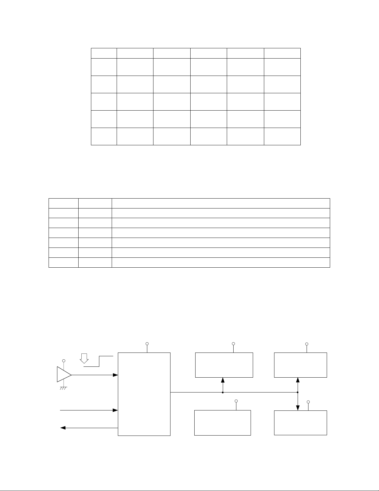
BUTTON MATRIX
KO0 3021
KO1 Control Demo Effect MIDI
KO2 +978
KO3 6-54
KI1 KI2 KI3 KI4 KI5
KO4 Tone
MIDI
Channel
Channel
On/Off
Octave
Shift
Modulation
POWER SUPPLY CIRCUIT
The power supply circuit generates six voltages as shown in the following table. VDD voltage is always
generated. The others are controlled by APO signal output from the CPU.
Name Voltage For operation of
VDD +5 V CPU, Reset IC, Working storage RAM
DVDD +5 V DSP, Key touch LSI, Sound source ROM, Effect RAM, KO siginal generator
AVDD +5V DAC, Filter
LVDD +4.5 V LED Driver
VCC +9 V Power amplifier, Pilot lamp
VC +9 V Power amplifier
RESET CIRCUIT
When batteries are set or an AC adapter is connected, the reset IC provides a low pulse to the CPU.
The CPU then initializes its internal circuit and clears the working storage RAM.
When the power switch is pressed, the CPU receives a low pulse of POWER signal. The CPU provides
APO signal to the power supply circuit and raises RESET signal to +5V to reset the DSP, the key controller and the KO signal generator.
Battery set
VDD
RESET
Reset IC
IC105
RH5VL36AA
POWER
From power switch
APO
To power supply circuit
VDD
CPU
LSI106
HD6433298A42F
-NMI
P42
-RESET
— 10 —
DVDD
KO Signal Generator
IC102
TC74HC174AF
VDD
Working Strage RAM
LSI105
SRM2264LM90
DVDD
DSP
LSI102
HG51B155FD
DVDD
Key Controller
LSI107
HG52E35P
Page 11
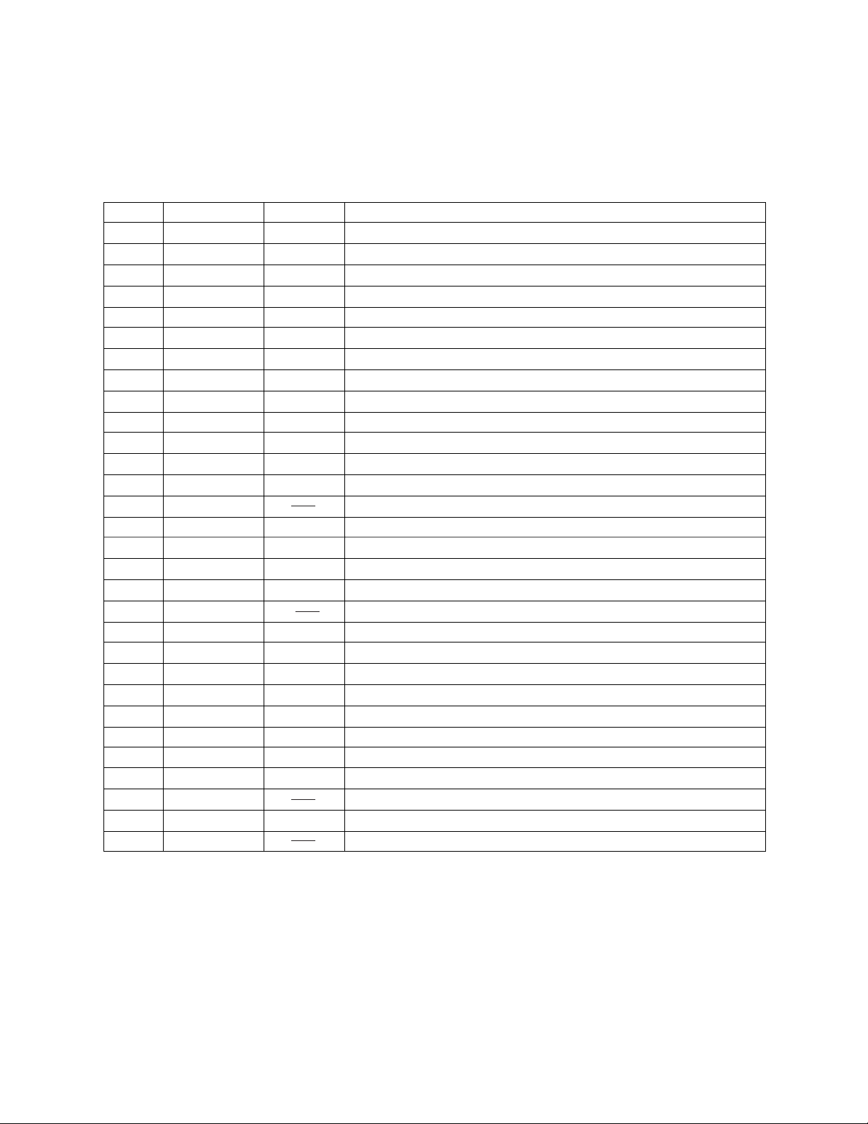
CPU (LSI106: HD6433298A42F)
The 16-bit CPU contains a 32k-bit ROM, a 1k-bit RAM, seven 8-bit I/O ports, an A/D convertor and MIDIl
interfaces. The CPU accesses to the working storage RAM, the DSP and the key touch LSI. The CPU
interprets MIDI message using the working storage RAM. The CPU also controls buttons and LEDs.
The following table shows the pin functions of LSI106.
Pin No. Terminal In/Out Function
1 P50/TXD Out MIDI signal output
2 P51/RXD In MIDI signal input
3 P52/SCK Out Reset signal output
4 -RESET In Reset signal input
5 -NMI In Power ON trigger signal input
6 VCC In +5V source
7 -STBY In Standby signal input. Connected to +5V.
8 VSS In Ground (0V) source
9, 10 XTAL, EXTAL In 20MHz clock input
11, 12 MD1, MD0 In Mode selection input
13 AVSS In Ground (0V) source
14 P70 In Analog input terminal for the pitch bend wheel
15 P71 In APO cancellation signal input
16 P72 Not used. Connected to +5 V source.
17 ~ 21 P73 ~ P77 Out LED drive signal output
22 AVCC In +5V source
23 ~ 30 P60 ~ P67 Out LED drive signal output
31 VCC In +5V source
32 P27 Not used
33 ~ 48 A0 ~ A14 Out Address bus
40 VSS In Ground (0V) source
49 ~ 56 D0 ~ D7 In/Out Data bus
57 P40 Out Clock for KO signal generator
58 P41 Out KO signal data
59 P42 Out APO signal output
60 P43 Out Read enable signal output
61 P44 In Write enable signal output
62 P45 Not used
63 P46 Out 10 MHz clock output
64 P47 Not used. Connected to +5 V source.
DIGITAL SIGNAL PROCESSOR (LSI102: HG51B155FD)
Upon receipt of note numbers and their velocities, the DSP reads sound and velocity data from the sound
source ROM in accordance with the selected tone; the DSP can read rhythm data simultaneously when a
rythm pattern is selected. Then it provides 16-bit serial signal containing data of the melody, chord, bass,
and percussion to the DAC. When an effect selected, the DSP adds the effect to the sound data using a
256k-bit RAM.
The following table shows the pin functions of LSI102.
— 11 —
Page 12

Pin No. Terminal In/Out Function
1 ~ 8 CD0 ~ CD7 In/Out Data bus
9, 10 CE1, TRSB Not used
11 GND7 In Ground (0V) source
12 CK16 Out Terminal for 24.576 MHz clock check point
13 VCC1 In +5V source
14 CK0 In Clock input. Connected to terminal CK16.
15 TCKB Not used
16 VCC1 In +5V source
17 GND1 In Ground (0V) source
18, 19 XT0, XT1 In/Out 24.576 MHz clock input/output
20 SGL In System control terminal. Single chip system: Open
21 CCSB In Chip select signal input
22 ~ 25 CA0 ~ CA3 In Address bus
26 CE0 In Not used. Connected to ground.
27 CWRB In Write enable signal
28 CRDB In Read enable signal
29 ~ 32 Not used
33 RESB In Reset signal input
34 TESB In Not used. Connected to +5V.
35 ~ 39 Not used
40 ~ 49
52 ~ 57
RD0 ~ RD15 In Data bus for the sound source ROM
50 VCC2 In +5V source
51 GND2 In Ground (0V) source
58 RA23 Out Not used
59 RA22 Out Chip select signal for the sound source ROM
60, 61 RA20, RA21 Out Not used
62 ~ 73
75 ~ 82
RA0 ~ RA19 Out Address bus for the sound source ROM
74 GND5 In Ground (0V) source
83 WOK2 Out Not used
84 VCC3 In +5V source
85 GND3 In Ground (0V) source
86 WOK1 Out Word clock for the DAC
87 SOLM Out Not used
88 SOLP Out Serial sound data output
89 BOK Out Bit clock output
90 ~ 92 Not used
93 VCC5 In +5V source
94, 95
97 ~ 105
107,109
EA0 ~ EA12 Out Address bus for the effect RAM
110, 112
96 EWEB Out Write enable signal for the effect RAM
— 12 —
Page 13

Pin No. Terminal In/Out Function
106 EOEB Out Read enable signal output for the effect RAM
108 VCC7 In +5V source
111 ECEB Out Chip select signal output for the effect RAM
113 ~ 117 ED11 ~ ED15 Not used
118 VCC4 In +5V source
119 GND4 In Ground (0V) source
120 ~ 122 ED8 ~ ED10 Not sued
Not used
123 ~ 130 ED0 ~ ED7 In/Out Data bus for the effect RAM
131 GND5 In Ground (0V) source
132 ~ 134 Not used. Connected to ground.
135, 136 Not used
Block diagram of DSP and DAC circuit
Sound Source ROM
LSI101
TC5316200CF-C112
CE
A0 ~ A19 D0 ~ D15
RA22
RA0 ~
RA19
RD0 ~
RD15
SOLP: Sound data
BOK: Bit clock
WOK1: Word clock
A12
A14
RD
APO
WR
RESET
D0 ~ D7
A0 ~ A3
CCSB
CRDB
CWRB
RESB
ECEB EOEB
OE
CS
Effect RAM (256K-bit)
DSP
LSI102
HG51B155FD
EWEB
WE
ED0 ~
ED15
D0 ~ D15
LSI103
LC33832M-70
EA0 ~
EA14
A0 ~ A14
SOLP
BOK
WOK1
DAC
LSI104
SI
CLK
LRCK
UPD6376GS
PG
X101
24.576 MHz
ROUT
LOUT
— 13 —
Page 14

DAC (LSI104: UPD6376GS)
The DAC receives 16-bit serial data output from the DSP. The data contains digital sound data of the
melody, chord, bass, and percussion for the right and left channels. The DAC converts the data into
analog waveforms by each channel and output them separately.
The following table shows the pin functions of LSI1.
Pin No. Terminal In/Out Function
1 SEL In Mode selection terminal. Connected to ground.
2 D.GND In Ground (0V) source for the internal digital circuit
3 NC Not used.
4 DVDD In +5V source for the internal digital circuit
5 A.GND In Ground (0V) source for the right channel
6 R.OUT Out Right channel sound waveform output
7, 8 A.VDD In +5V source for the internal analog circuit
9 R.REF In Right channel reference voltage terminal
10 L.REF In Left channel reference voltage terminal
11 L.OUT Out Left channel sound waveform output
12 A.GND In Ground (0V) source for the left channel
13 LRCK In Word clock input
14 LRSEL In Not used. Connected to ground.
15 SI In Sound data input
16 CLK In Bit clock input
KEY CONTROLLER (LSI107: HG52E35P)
The key controller generates key scan signals and provides them to the keyboard. By counting the time
between first-key input signal FI and second-key SI from the keyboard, the key controller detects key
velocity. The note number and its velocity data are read at regular intervals by the CPU.
Key Controller
RD
APO
WR
CLOCK
A13
A14
RESET
Data bus
Address bus
LSI107
HG52E35P
CRDB
CWRB
CKI
CCSB
RESB
CD0
CD7
CA0 ~ CA2
SI0
SI7
KC0
Key scan signal
~
KC7
FI0
Key input signal
FI7
Keyboard
KC
First contact
FI
SI
Second contact
— 14 —
Page 15
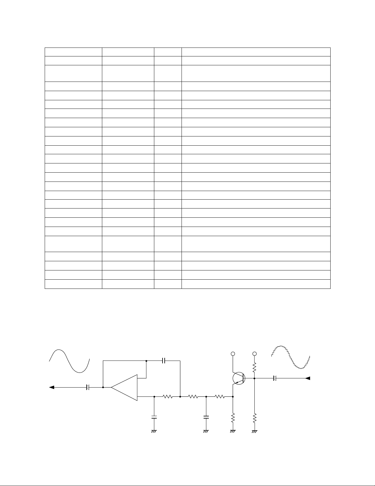
The following table shows the pin functions of LSI107.
Pin No. Terminal In/Out Function
1 REQB Out Not used
2, 3, 60 ~ 63
FI8 ~ FI10,
SI8 ~ SI10
In Not used. Connected to + 5V.
4 VCC In +5V source
5 CRDB In Read enable signal input
6 CWRB In Write enable signal input
7 CCBB In Chip select signal input
8, 9, 11 T, STBY, W In Not used. Connected to +5V.
10 RESB In Reset signal input
12 CKI In 10 MHz clock input
13, 14 TMD, TST In Not used. Connected to ground.
15 CKO Out Not used.
16 GND In Ground (0V) source
17 XIN In Not used. Connected to ground.
18 XOUT Out Not used.
19 TRES In Not used. Connected to ground.
20 ~ 23, 25 ~ 28 CD0 ~ CD7 In/Out Data bus
24 GND In Ground (0V) source
29 ~ 31 CR0 ~ CR2 In Address bus
32 VCC In +5V source
33 ~ 39, 41 ~ 43
53 ~ 55, 57 ~ 59
FI0 ~ FI7,
SI0 ~ SI7
In Key input signal input
40 VCC In +5V source
44 ~ 47, 49 ~ 52 KC0 ~ KC7 Out Key scan signal
48, 56 GND In Ground (0V) source
64 VCC In +5V source
FILTER BLOCK
Since the sound signals from the DAC are stepped waveforms, the filter block is added to smooth the
waveforms.
10V22µ
To main volume
IC105
M5218APR
-
+
C333(H)
1K
C222(H)
AG
AVDD
Q107/108
2SC1740
1K 1K
C103(H)
AG
— 15 —
1K
AG
AVDD
18K
1K
AG
50V1µ
From the DAC
Page 16

POWER AMPLIFIER (IC402: LA4598)
The power amplifier is a two-channel amplifier with standby switch.
The following table shows the pin function of IC402.
Pin No. Terminal In/Out Function
1 Power GND In Ground (0V) source
2 Ch1 B.S. Terminal for a bootstrap capacitor
3 Ch1 OUT Out Channel 1 output
4 VCC In +9V source
5 Ch1 N.F. In Negative feedback input
6 Ch1 IN In Channel 1 input
7 D.C. Terminal for a decoupling capacitor
8 Pre GND In Ground (0V) source
9 Stand by In Power control signal input. 0 V: Off, +9 V: On
10 Ch2 IN In Channel 2 input
11 Ch2 N.F. In Negative feedback input
12 Ch2 OUT Out Channel 2 output
13 Ch2 B.S. Terminal for a bootstrap capacitor
14 NC Not used
LED DRIVING
IC371
BA612
LED Driver
LG
La ~ Lg, Lp
KP0 ~KP5
(KO0 ~ KO5)
LVDD
Q104 ~Q111
LED Driver
IC102
TC74HC174AF
KO Signal Generator
LS0 ~ LS7
CPU
LSI106
HD6433298A42F
P40
P41
— 16 —
Page 17

MAJOR WA VEFORMS
1
2
CH1: CH2:
Voltage VDD
1
CG connector pin 6
Initial reset signal
2
RH5VL36A pin 1
A . 1 s
CH1
3
4
CH2
5
5 V5 V
3
4
5
5 VCH1: CH2:
Power ON signal PSW
HD6433298A42F pin 5
APO signal
HD6433298A42F pin 59
Reset signal
HD6433298A42F pin 3
5 V
A . 1 s
CH1
CH2
B
C
D
5 VCH1: 5 VCH2: 5 VCH3:
Word clock WOK1
B
UPD6376GS pin 13
Data S1 (Note OFF)
C
UPD6376GS pin 15
Bit clock BOK
D
UPD6376GS pin 16
A 1 µs
CH1
CH2
CH3
E
F
CH1: 20 mV~CH2: 20 mV
Filter output AOR
E
CG connector pin 3
Filter output AOL
F
CG connector pin 4
Tone :
Key :
Touch response :
Whistle (No. 078)
A4
OFF
A 1 ms
CH1
CH2
~
6
7
8
5 VCH1: 5 VCH2: 5 VCH3:
Key scan signal KC0
6
HG52E35P pin 44
Key scan signal KC1
7
HG52E35P pin 45
Key scan signal KC2
8
HG52E35P pin 46
A 20 µs
CH1
CH2
CH3
9
0
A
5 VCH1: 5 VCH2: 5 VCH3:
Button scan signal KO0
9
CE connector pin 1
Button scan signal KO1
0
CE connector pin 2
Button scan signal KO2
A
CE connector pin 4
A 10 ms
CH1
CH2
CH3
G
CH1:
5 V
MIDI signal output
G
CG connector pin 16
A . 1 ms
Note OFF
CH1
Note ON
— 17 —
Page 18

AMP./VOLUME PCBs JCM715-MA2M/MA3M
SCHEMATIC DIAGRAMS
— 18 —
Page 19

MAIN PCB JCM715-MA1M
17
2
16
15
3
13
14
5
12
1
4
9
10
11
6 7 8
— 19 —
Page 20

CONSOLE PCBs JCM715-CN1M/2M/3M
— 20 —
Page 21

KEYBOARD PCBs M616T-KY1M/KY2M
— 21 —
Page 22

14
EXPLODED VIEW
11
12
13
10
11
7
1
9
8
16
3
6
15
17
19
— 22 —
18
20
2
20-1
22
24
20-2
4
23
21
5
Page 23

PARTS LIST
GZ-500
Notes: 1. Prices and specifications are subject to change with-
out prior notice.
2. As for spare parts order and supply, refer to the
"GUIDEBOOK for Spare parts Supply", published
seperately.
3. The numbers in item column correspond to the same
numbers in drawing.
Page 24

FOB Japan
N Item Code No. Parts Name Specification Q N.R.Yen R
Unit Price
Main PCB
N1
6923 6180 PCB ass'y M715-MA1M M140244*1
1
7,810 A
N LSI101 2012 1498 LSI TC5316200CF-C117 1 980 A
N LSI102 2012 1316 LSI HG51B155FD-1 1 1,160 A
N LSI103 2012 0777 LSI LC33832M-70-TLM 1 410 A
N LSI104 2114 4221 LSI UPD6376GS-E1 1 200 A
N LSI105 2012 0770 LSI SRM2264LM90-B 1 280 A
N LSI106 2012 0462 LSI HD6433298A42F 1 860 A
LSI107 2011 5194 LSI HG52E35P 1 600 A
N IC101 2114 4214 IC M5218AFP-600C 1 39 B
N IC102 2105 4452 IC HD74HC174FPTR 1 51 B
N IC103 2105 3122 IC HD74HC00FP-TR 1 35 B
N IC104 2105 4445 IC HD74HC08FPTR 1 34 B
N IC105
2105 4536 IC RH5VL36AA-T1
1
44 B
N Q101, Q102 2252 1169 Chip transistor 2SC4081-T106S 2 8 B
N Q103 ~ Q111 2250 1169 Chip transistor 2SA1576AT106S 9 8 B
N D101 2390 1729 Chip diode RB411DT146 1 24 C
N D102 2390 1820 Chip diode 1SS355TE-17 1 9 C
N X101 2590 2107 Crystal oscillator HC-49S24A 1 130 B
N X102 2590 2100 Ceramic oscillator CSACS20.00MX040-TC 1 70 B
Amp./Volume PCBs
N 2 6923 6190 PCB ass'y M715-MA2,3M M140245*1 1 2,350 B
IC401 2105 2114 IC, Regulator S-81350HG 1 65 A
IC402 2114 2891 IC LA4598 1 140 A
IC403 2114 1421 IC, Photocoupler PC900V 1 210 B
Q401, Q404 2220 1387 Transistor 2SC1740SQ-TP-T 2 13 A
Q402 2253 0581 Transistor 2SD1858R.S-TV6-T 1 24 A
Q403 2251 0665 Transistor 2SB1240R.S-TV6-T 1 26 A
Q405 2251 0651 Transistor 2SB1274-CCC 1 47 A
Q406 2200 4409 Transistor 2SA933-SQ-TP-T 1 14 B
D401 2360 0098 Zener diode RD5.1ESB2-T1-T 1 14 A
D402 2360 2261 Zener diode RD5.1JSB3-T1-T 1 9 A
D403,
2390 1344 Diode 1SS133T-77-T
4
3C
D407~D409
D404 2310 7996 Zener diode RD4.7ESB2-T1-T 1 12 B
N D405 2390 2408 Diode 1FWJ43N(TPA3) 1 27 C
D406 2390 0371 Diode DSK10B-BT-T 1 11 C
J101
J102
J103
J104
VR101
3501 7049 Power jack HEC2305-01-330
3612 0665 Phone jack YKB21-5006
3612 0789 Jack YKB21-5010
3501 4816 DIN jack YKF51-5051
2765 1575 Slide volume EWA-MJ0S10B23
1
1
1
1
1
29 A
60 B
60 B
110 B
110 B
Console PCBs
N 3 6923 6200 PCB ass'y M715-CN123M M240232*1 1 1,170 B
IC371 2114 3318 IC BA612 1 98 B
D372~D391
2390 1344 Diode 1SS133T-77-T
21
3C
N LED371/372 2370 1197 LED MVR3378S-B102 2 18 C
LED373 2370 0959 LED LN882RPX-(TT) 1 27 C
LED374 2370 1141 LED SL-9352-60 1 200 B
LED375
2370 0987 LED LN28RPX-(TT14)
1
17 C
Keyboard PCBs
N 4 6923 6240 PCB ass'y M616T-KY1M M111750*3 1 870 B
2301 0101 Diode 1S2473-T-77-T 64 8 C
N 5 6923 6250 PCB ass'y M616T-KY2M M111751*3 1 830 B
Notes: N – New parts
M – Minimum order/supply quantity
R – Rank
— 23 —
Page 25

FOB Japan
N Item Code No. Parts Name Specification Q N.R.Yen R
Unit Price
2301 0101 Diode 1S2473-T-77-T 58 8 C
Bender
VR102 2765 1141 Rotary volume RK1631110-50KB 1 190 B
N 6 6923 6450 Bender knob M340169-2 1 60 C
Mechanical Parts
N
7 6906 7781 Rubber button, Light gray M312088A-3 1
N 8 6923 6420 Rubber button, White M312125-3
N 9 6923 6410 Rubber button, Gray M312123-3
N 10 6923 6400 Rubber button, Pink M312122-3
N
11 3831 0357 Speaker 1221AF 2
N 12 6923 6390 Top panel M140150-1
N
N
13 6923 6430 Slide knob M311860-2 1
14 6923 6381 Display plate M340172A-1 1
15 6922 2840 White key set, CEGB M111723-1
16 6922 2850 White key set, DFA M111724-1
17 6922 2860 White key set, DFAS M111725-1
18 6922 2740 Black key set,10-key M111726-1
19 6922 2750 Black key set, 5-key M111726-2
N 20 6906 7805 Case M111732E*3
20-1 6902 6140 Battery spring M41226-1
20-2 6903 2150 Battery spring M41330-1
21 6922 2761 Key contact rubber LT-CB M211704A-1
22 6922 2771 Key contact rubber LT-CS M211705A-1
23 6922 2631 Bottom plate M211706A-1
N
24 6906 7876 Battery cover M311164F*9 1
2
1
1
1
5 100 A
4 100 A
1 100 A
2 120 A
186A
1
1
1
489B
191B
1
97 B
67 B
28 B
28 B
1,000 B
1,340 C
13 B
170 C
1,340 C
27 C
18 C
360 C
180 B
Accessory
6920 8691 Music stand M311760A-1 1 130 B
Notes: N – New parts
M – Minimum order/supply quantity
R – Rank
— 24 —
Page 26

MA0800751A
 Loading...