

Page 1

1. Operations of P.C.B.s
(1) Main P.C.B.
• Syscon servo section
1 IC100 main microcomputer : Servo, video, audio control and system control
2 IC101 RESET : Main microcomputer reset
3 IC200 E3V REG & RESET E3V : Regulator, MODE microcomputer reset
4 IC201 EEPROM : EEPROM for recorder data
5 IC202 LANC INTERFACE : LANC interface
6 IC203 SUB MICON : Charging and main power control
7 IC300 MOTOR DRIVE : Drum, capstan, loading motor driver
8 IC301 5.6V REGULATOR : 5.6 V regulator for motor driver
• Video section
1 IC2000 VRP2 : Recording/playback head amplifier
2 IC2100 VIF2 : Analog video input/output signal processing
3 IC2301 VIC2 : Digital VCR signal processing LSI (with built-in SDRAM)
• Audio section
1 IC801 AUDIO INTERFACE : Analog audio input/output signal processing
2 IC802 A/D, D/A CONVERTER : Audio signal A/D, D/A conversion
• Camera section
1 IC1101 DIC2S : Camera digital signal processing (DIC+FIC)
2 IC1400 RESET : Camera microcomputer reset
3 IC1401 CAMERA MICOM : Camera control
4 IC1402 EEPROM : EEPROM for camera data
• CVF section
1 IC1502 EVF DRIVER : CVF, LCD drive
2 IC1504 EVR (D/A CONVERTER) : D/A converter for CVF (EVR)
ZR10A
CHAPTER 2. TECHNICAL DESCRIPTION
(2) PMCA P.C.B.
• Camera section
1 IC1005 TIMING GENERATOR : Timing generator for CCD drive
2 IC1006 CDS/AGC/AD : Sampling, AGC and A/D conversion of CCD output signal
3 IC1300 MOTOR DRIVER : AF/PZ motor driver
4 IC1450 EVR (D/A CONVERTER) : D/A converter for camera adjustment (EVR)
• PM section
1 IC3201 DC/DC CONVERTER CONTROL : PWM regulator controller for power supply
2 IC3202 SWITCHING REGULATOR : PWM regulator controller for power supply
3 IC3203 4.7V REGULATOR : 4.7 V regulator for video, audio and digital circuit
4 IC3205 5V REGULATOR : 5 V regulator for speaker
5 IC3206 5V REGULATOR : 5 V regulator for charger circuit
6 IC3207 CHARGE CONTROL : Charge control circuit
7 IC3219 2.8V REGULATOR : 2.8 V regulator for DIF (inside VIC)
(3) JACK P.C.B.
1 IC1671 P SENSOR GYRO : Velocity detection in the direction of PITCH
2 IC1672 Y SENSOR GYRO : Velocity detection in the direction of YAW
2-3
Page 2

ZR10A
CHAPTER 2. TECHNICAL DESCRIPTION
(4) LCD P.C.B.
1 IC901 EEPROM : EEPROM for LCD data
2 IC902 DA CONVERTER : D/A converter for LCD (EVR)
3 IC903 LCD INTERFACE : LCD signal processing
4 IC904 LCD CONTROLLER : LCD drive
5 IC4201 DC/DC CONVERTER : DC/DC converter for backlight
(5) CVF P.C.B.
For relaying signals from the MAIN P.C.B. to CVF-LCD and the backlight circuit to drive LED.
2-4
Page 3
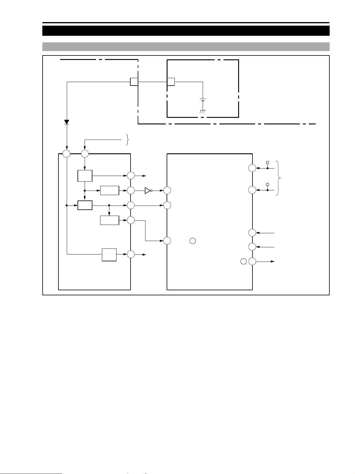
2. Power Circuit
2-1 Starting Up The Power Circuit
ZR10A
CHAPTER 2. TECHNICAL DESCRIPTION
MAIN P.C.B.
LITHIUM 3V
UNREG VTR
3
E3V REG.
7
3V
REG.
SW
IC200
RESET
DET
RESET
2.6V
DET.
CN201
20
FROM
BATTERY
8
4
6
5
2
E3V
3V
LI3 DET
MAIN MI-COM
36pin
CN250
1
E3V DET
4
43
VCC
15
RESET L
IC203
SUB MI-COM.
LI P.C.B.
LITHIUM
BATTERY
CASSETTE IN SW
*
VTR PW SW
CAM PW SW
EJECT SW
VTR ON H
26
25
20
21
48
TP203
TP202
FROM
POWER SW
FROM DMC
FROM FRONT
COVER
TO PMCA P. C.B.
Fig. 2-1
• About The Lithium Battery Used as Backup Power Supply
The LITHIUM 3V is supplied to pin 3 of IC200. Then Vcc is supplied from pin 6 of IC200 to pin 43 of the SUB
microcomputer. Thereby, various data and date/time information are backed up by the 3 V lithium battery when the
main power is not supplied. Output signal from pin 2 of IC200 indicates decrease of the 3V lithium battery voltage.
When a lithium battery is not installed or its voltage decreases 2.6 V or less, this signal goes “L” that is sent to pin 36
of the MAIN microcomputer. Upon receiving this signal, the MAIN microcomputer issues a warning indication
telling low voltage of lithium battery.
• When The Main Power Is Connected
When the main power is connected, the UNREG. VTR power is supplied to pin 7 of IC200. The UNREG. VTR power
is converted to 3 V by an internal regulator. The 3 V regulated power is supplied to external circuits from its pin 8 as
the EVER 3 V power. Also, by means of internal selector, the regulated 3 V power is output from pin 6. The output
from pin 4 of IC200 serves as a main power detection signal. Result of the detection of the EVER 3V power is sent to
the SUB microcomputer whether the main power is connected or not. Then the SUB microcomputer performs initial-
ization of the system and enters the standby state. When the POWER switch is turned on in the above standby state
with the main power connected, any of pins 25 or 26 of the SUB microcomputer goes LOW that turns on the main
power. Each circuit starts up by outputting the VTR ON “H” signal (pin 48) to the PMCA P.C.B. When voltage at pin
6 of IC200 decreases 2.4 V or less, output from pin 5 of IC200 goes “L” thereby resetting the SUB microcomputer.
2-5
Page 4
ZR10A
CHAPTER 2. TECHNICAL DESCRIPTION
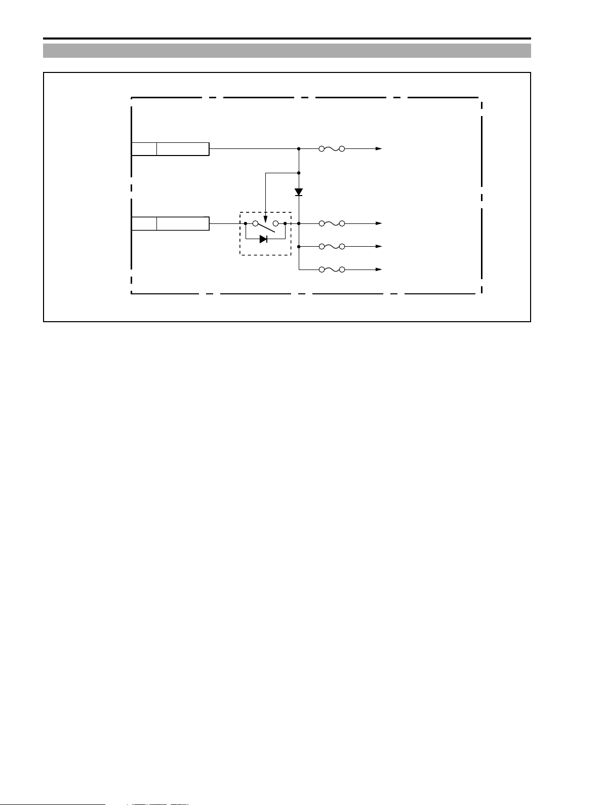
2-2 Power Fuse
PMCA P.C.B.
FROM
ADAPTER
FROM
BATTERY
TERMINAL
7–10
12–15
CN3201
DC IN
CN3201
BATT +
Q3217
FU3204
UNREG (CHARGE)
D3207
FU3201
UNREG 1
FU3202
UNREG 2
FU3203
VS UNREG
Fig. 2-2
The main power supplied from the battery terminal is distributed to the three power lines as described below through the
three power fuses (FU3201, FU3202 and FU3203) via a switch Q3217 that turns off the battery power when an external
DC input (from AC adaptor) is supplied.
The external DC input (from AC adaptor) takes the two routes. One route is connected to the charger circuit via FU3204
and the other route is connected to the three power fuses and is distributed to the three power lines same as the battery
power via D3207 that prevents the reverse current.
(1) UNREG (CHARGE) : FU3204
Power for the charger circuit
(2) UNREG1 : FU3201
Power for the camera and recorder circuits. (except 5V)
(3) UNREG2 : FU3202
Power for LCD, Backlight, E3V, Motor driver and Speaker
(4) VS UNREG : FU3203
Power for drum/capstan VS, camera recorder circuits. (5V)
2-6
Page 5
ZR10A
CONTROL
CTL1
CTL2
CH-1
CH-2
CH-3
CH-4
HHLH
L
: ON : OFF
IC3201
DC/DC
CONVERTER
CONTROL
CH-1
CTL1
CTL2
CH-3
CH-4
CH-2
CH-1
OSC
Q3212
Q3203
Q3204
Q3216
Q3215
Q3214
Q3210
Q3209
Q3213
VTR ON H
CAM ON H
VTR ON H
ON H
IC3202
SWITCHING
REG.
PWM
PWM
UNREG 1
UNREG 1
T3202
T3201
Q3202
REG.
DIF 2.8V
CP 5.0V
AVDD 2.3V
DVDD 1.7V
HA 3.0V,
DVDD 3.0V,
A 3.0V, SD 3.0V,
LCD 3.0V
IS 3.0V
CAM 3.0V
LCD 15V
AL –10.0V
CCD 12V
CCD –6.5V
LPF
LPF
LPF
LPF
LPF
30
1
6
5
2
4
50
33
56
19
57
14
3
7
15
10
36
29
39
46
LPF
LPF
LPF
LPF
LPF
LPF
LPF
CH-2
REG.
REG.
DVDD 2.2V
LPF
UNREG 1
UNREG 1
UNREG 1
VS UNREG
UNREG 2
REG.
1
6
5
2
4
-
54
3
AUD ON
SP 5.0V
IN OUT
ON
45
1
IN OUT
ON
21
IN OUT
IC3205
5V REG.
IC3203
4.7V REG.
IC3219
2.8V REG.
A 4.7V, V 4.7V,
DVDD 4.7V
VIF 4.7V
POW 5.0V,
LCD 5.0V
CHAPTER 2. TECHNICAL DESCRIPTION
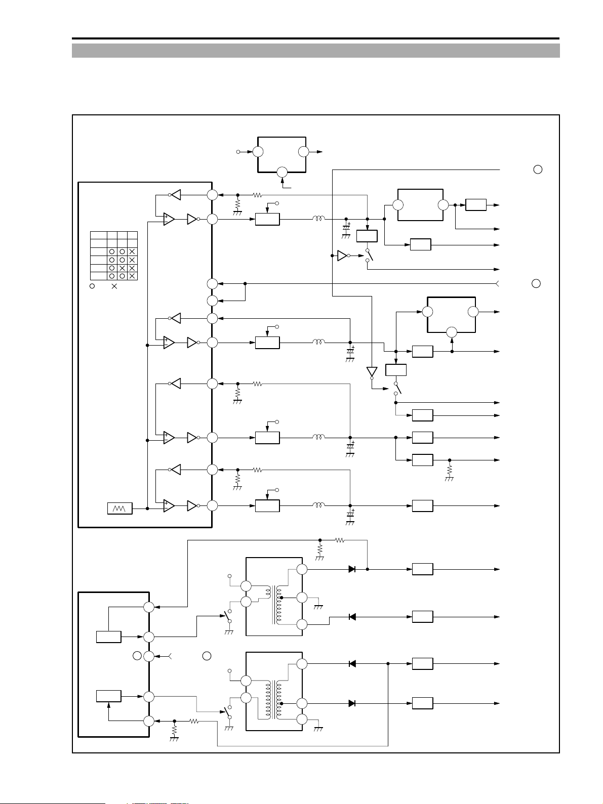
2-3 Power Supply Circuit
Power supply circuit is shown in Fig. 2-3.
Turning ON/OFF the respective powers is controlled by the CAMER ON “H” and VTR ON “H” output signals that are
supplied from the SUB microcomputer. (IC203).
Fig. 2-3
2-7
Page 6
ZR10A
CHAPTER 2. TECHNICAL DESCRIPTION
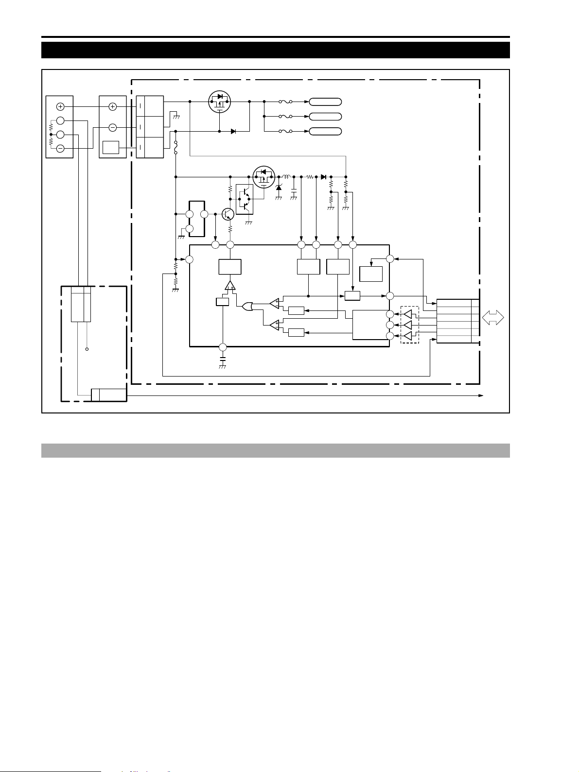
3. Built-in Charger Circuit
BATTERY BATT FPC
B
D
DC
JACK
1
2
FN251
BATT INFO
BATT– E3
AD
LI P.C.B.
E3V
12
15
1
5
7
10
CN3201
BATT +
GND
DC IN
FU3204
IC3206
TK71550S
5V REGURATOR
VCC
132
12
VCC
Q3211
5V
10 1920 21 231
REF IN
DC IN OFF
OUTPUT
DRIVE
DSC
3
Q3217
Q3220, Q3224
Q3225
IC3207
M6225FP
CHARGE
CONTROL
FU3201
FU3202
FU3203
VREF
VREF
R3261
I
DETECT
UNREG 1
UNREG 2
VS UNREG
DETECT
PMCA P.C.B.
PS
POWER
SAVE
D OUT
DATA IN
5
15
CK
6
7
CS
8
IC3204
CN1002
D OUT
PS
CHG CLK
CHG DATA
CHG CS
DC J DET
SUB
67
MI-COM
69
75
73
71
65
V
AMP
CN250
BATT INFO
18
AD
Fig. 2-4
3-1 Outline
The main circuit elements and their functions are as follows.
(1) SUB microcomputer
• Control of IC3207 (serial data communication)
• Detection and display of charging progress
• Error discrimination and display
• Battery type discrimination and DC jack input detection
(2) IC3207 (CHARGE CONTROL)
• Charging voltage and charging current control
SUB
MI-COM
2-8
Page 7
ZR10A
CHAPTER 2. TECHNICAL DESCRIPTION
3-2 Operation at Charging
3-2-1 Conditions To Start Charging
When the following conditions are satisfied, the MODE microcomputer (IC203) controls IC3207 using serial data com-
munication and starts charging.
Conditions Detection Source of detection
Main unit power is turned OFF or is in the VCR STOP mode SUB MI-COM —
DC voltage of 8.8 V or higher is input to the external SUB MI-COM pin 19 DC IN
DC terminal DCJACK DET (CN3201 pin 7-10)
Battery is installed (FN251 pin 2 at 0.6V or higher) SUB MI-COM pin 41 Battery D terminal
BATT. INFO A/D (FN251 pin 2)
3-2-2 Progress of Charging
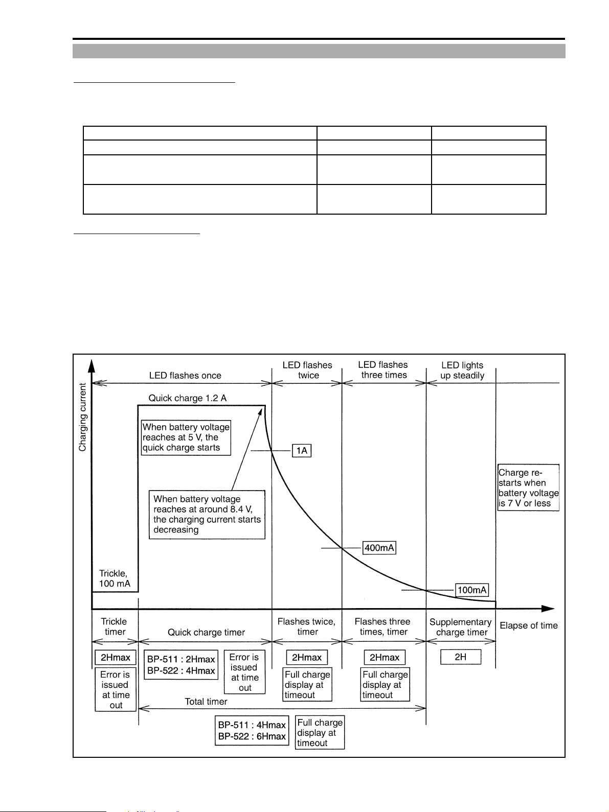
IC3207 starts a trickle charge following the instructions from the SUB microcomputer (IC203). The trickle charge contin-
ues until battery voltage reaches 5 V. When a battery voltage reaches 5 V, a quick charge of 1.2A starts. Amount of charge
current decreases gradually as a charge advances (because battery impedance increases as a charge advances). When
charging current reaches 100 mA or less, the “end of charging” indication appears. After that a supplementary charge is
performed for two hours. Thus charging completes. Note that the same charge control is performed in this model in both
the VCR STOP and POWER OFF modes that was different in preceding models. (It is realized because current capacity
is increased in the AC power adapter and charger circuit.)
Fig. 2-5
2-9
Page 8
ZR10A
CHAPTER 2. TECHNICAL DESCRIPTION
3-2-3 Charge Control
While charging is in progress, the SUB microcomputer (IC203) receives the data of charging voltage and charging current
from IC3207 pin 15 in order to carry out various controls.
(1) LED indication
Indication changes as a charging current changes as shown in Fig. 2-5.
(2) In the cases as described below, a battery is judged to have abnormality and charging is stopped. The LED changes to
an error indication.
1 When battery terminal voltage drops to 5 V or less during the quick charging mode.
2 When a trickle timer or a quick charge timer reaches its preset time.
(3) Timers
The specified operations are performed in accordance with the timer data and the charge status. Note that the total/
quick charging time varies with the capacity of the mounted battery. Battery capacity is identified from the D terminal
voltage (FN251 pin 2 : BATT INFO) of the battery installed in the unit.
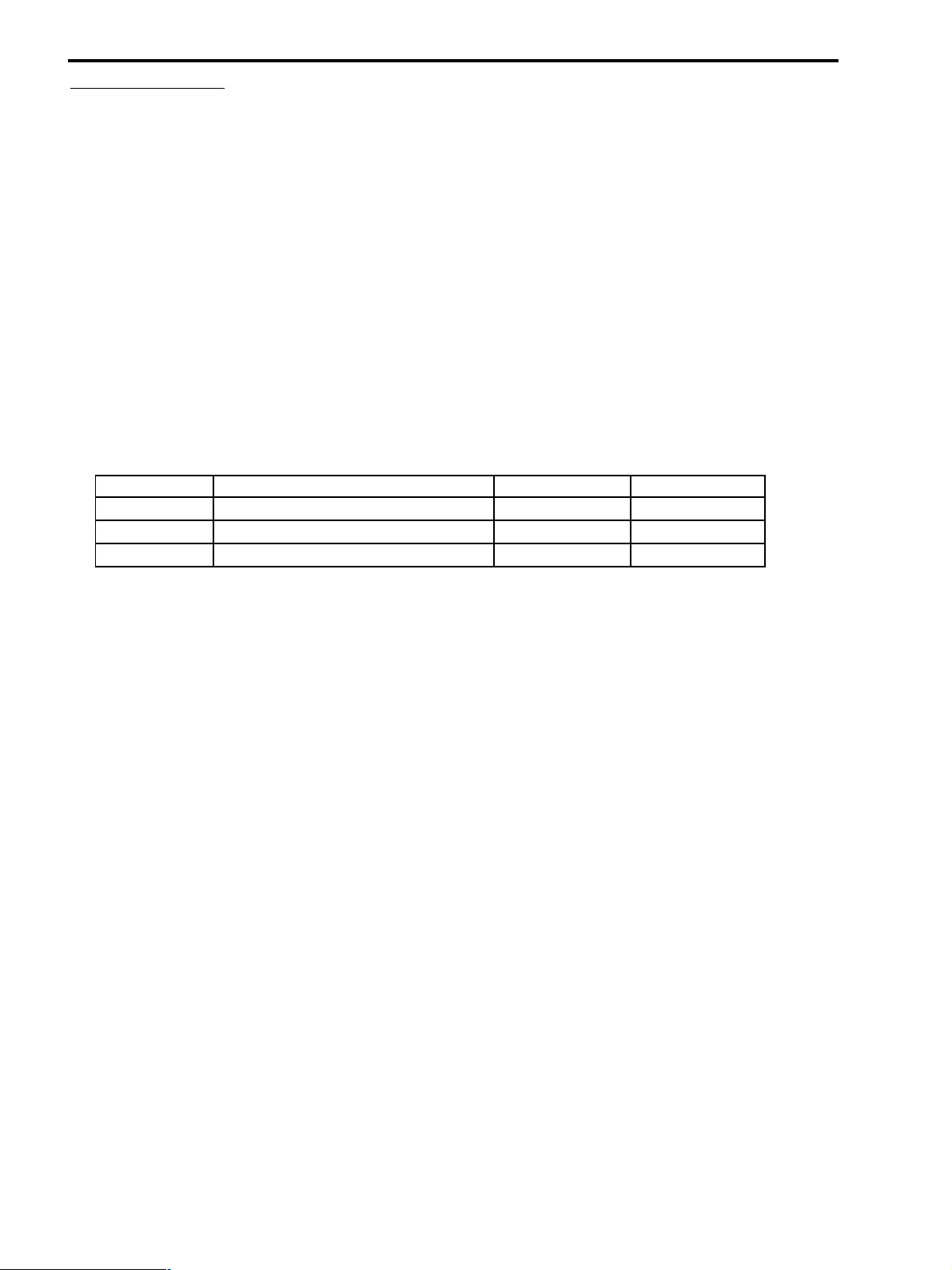
Battery installed D terminal voltage (FN251 pin 2 : BATT INFO) Quick charge timer Total timer
BP-511 2.1 V (within ±0.3 V) 2H 4H
BP-522 1.5 V (within ±0.3 V) 4H 6H
Not installed 0 V (within 0.6 V) ——
1 When a trickle timer or a quick charge timer reaches its preset time → Charge stops due to abnormal battery.
2 When a protection timer or a total timer reaches its preset time after the LED flashes twice → LED lights up
steadily, Supplementary charge starts.
3 When supplementary charge timer reaches its preset time after LED lights up steadily → Charging completes
while the LED lights up.
2-10
Page 9
CHAPTER 2. TECHNICAL DESCRIPTION
4. Signal Processing Circuit
4-1 Outline of Signal Processing Circuit
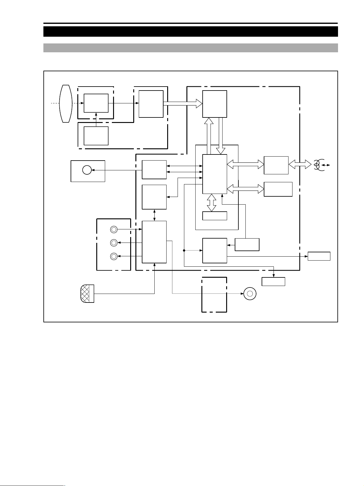
Overall block diagram of the signal processing circuit, and flow of video and audio signals are shown as follows.
CCD P.C.B.
IC1071
CCD
13.5MHz
IC1006
CDS
/AGC
/AD
10bit
13.5MHz
IC1101
DIC2S
MAIN P.C.B.
ZR10A
LENS
IC1005
TG
SJ FPC
S
S TERMINAL
JACK P.C.B.
MIC
EXT. MIC
HEADPHONE
A/V
PMCA P.C.B.
IC2100
VIF2
IC802
A/D
D/A
IC801
AIF
B DATA A DATA
8bit
27MHz
VIC 2
SDRAM
IC2301
IC1502
LCD
DRIVER
LI
P.C.B.
41.85Mbps
IC2600
CG
REC/PB
HEAD
IC2000
VRP2
DV
TERMINAL
CVF
LCD
SPEAKER
Fig. 2-6
2-11
Page 10
ZR10A
CHAPTER 2. TECHNICAL DESCRIPTION
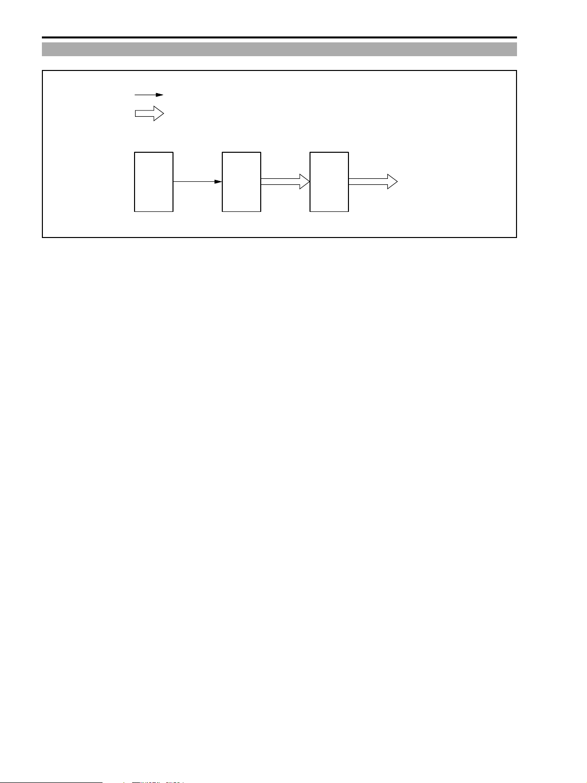
4-2 Camera Signal Processing
: ANALOG
: DIGITAL
IC1006
IC1071
CCD
13.5MHz
<CCD> IC1071
• 1/4 inch • Complementary color filter
• 460,000 pixels
CDS
/AGAC
/AD
10bit
13.5MHz
Fig. 2-7
IC1101
DIC2S
8bit
27MHz
TO
IC2301
VIC2
<CDS/AGC/AD> IC1006
• Signal read out from CCD passes through the sample-and-hold AGC processing and A/D conversion circuit.
Signal is output in a digital form.
<DIC2S> IC1101
• Performs Y/C separation, various camera signal processing, digital effect processing and EIS.
(Electronic Image Stabilizer)
(The DIC and FIC conventionally used are packed into one)
2-12
Page 11
SDRAM
SDRAM
INTERFACE
DIF
INTERFACE
IC1101
DIC2S
A DATA
B DATA
AV JACK
S TERMINAL
CVF
LCD
LCD
IC2100
VIF2
IC1502
LCD
DRIVER
VIDEO
INTERFACE
D/A
A/D
R,G,B
COMPRESSION
/DEMOD.
ECC
REC/PB
PROCESS
BUS
AUDIO
INTERFACE
IC2301 VIC2
DV
TERMINAL
IC2000
VRP2
VIDEO
HEAD
IC802
A/D
D/A
AV JACK
4-3 Recorder Block Signal Processing
ZR10A
CHAPTER 2. TECHNICAL DESCRIPTION
Fig. 2-8
<VIC2> IC2301
• Signal processing circuit of the recorder block is integrated with SDRAM into a single chip.
• A/D converter for analog LINE input signal and Y/C separation filter are built in.
• D/A output is newly added for VRP control.
• A/B DATA : Input data in the camera mode. During playback mode, the B DATA is output and A DATA is input.
(The DIC2S digital effect circuit is used during playback.)
The video data and signals input to VIC2 receive signal processing of the digital VCR format. Audio data, subcode
data and ITI data are created in VIC. These signals are output to VRP as 41.85 Mbps data of digital VCR format.
• DIF : Digital data output is converted to the standard IEEE1394 digital data and is output to the DV terminal.
During the digital input mode, the data enters the VIC2 signal processing circuit via a reverse route.
<VRP2> IC2000
• The 41.85 Mbps recording data that is output from VIC2 is amplified in VRP and is recorded on magnetic tape
while the recording data is switched by the switching pulse to be allocated to CH-1 and CH-2 recording heads.
During playback, the head output signal is amplified and sent to VIC2.
<VIF2> IC2100
• Related parts are reduced in comparison to conventional VIF, and a sync separation function for analog line input
is added. Y and C signals that are supplied from VIC2 are output as the Y and C signal outputs for S terminal and
composite video output signal.
During the line input mode, input signal receives level adjustment and sync signal separation, and is output to
VIC2.
<LCD DRIVER> IC1502
• LCD DRIVER, formerly mounted on CVF P.C.B., is moved to the MAIN P.C.B., and displays on CVF LCD an
image that is created from the R, G, B and sync signals supplied from VIC2.
2-13
Page 12
ZR10A
CHAPTER 2. TECHNICAL DESCRIPTION
4-4 Audio Signal Flow
IC701
MIC
AMP
L+R
L
R
L
R
IC802
A/D
D/A
SPEAKER
AMP
IC2301
VIC2
+
–
BEEP 1
IC2000
VRP2
REC/PB
SPEAKER
IC100
MAIN MI-COM
MIC
EXT.
MIC
HEAD
PHONE
AV
JACK
L
R
L
R
L
R
L
R
L
R
L
R
IC801
AIF
Fig. 2-9
<MIC AMP> IC701
• A microphone amplifier is constituted by an externally connected operational amplifier outside the AIF, with
which the dynamic range is expanded.
<AIF> IC801
• It selects the built-in microphone signal or an external microphone signal (in accordance with the serial data from
MAIN microcomputer). It also performs ALC (Auto Level Control), and amplification for various output signals.
The beep tone that sounds at ejection, etc., is generated from the signal that is supplied from the MAIN microcom-
puter and is added to the speaker output signal at AIF.
HEAD
<A/D, D/A> IC802
• It performs signal conversion between analog signal and digital signal. Sampling frequency Fs is output from
VIC2. Fs = 32 kHz or Fs = 48 kHz is selected depending on the audio mode. Number of quantization bits is 12 bits
in case of 32 kHz or 16 bits in case of 48 kHz.
2-14
Page 13
ZR10A
CHAPTER 2. TECHNICAL DESCRIPTION
5. System Control and Servo
5-1 Outline of System Control and Servo
Fig. 2-10 shows the overall block diagram of the system control & servo circuits with flow of data. System control is
mainly performed by the MAIN microcomputer (IC100) on MAIN P.C.B.
:Parallel Bus line :Serial Bus/Data line :Servo Signal/Other data
PMCA P.C.B. (1/2)
IC1005
TIMING
GENE.
IC1006
CDS/AGC/EVR
IC1101
DIC2S
IC1402
2
PROM
E
IC2600
CG
IC1502
LCD (CVF)
DRIVER
IC1501
D/A
CONVERTER
IC201
2
PROM
E
IC202
LANC
I/F
LENS
IC1300
MOTOR DRIVER
IC1401
CAMERA
MI-COM
IC100
MAIN
MI-COM
MAIN P.C.B. DMC II
DRUM
FG/PG
CAPSTAN
LOADING
MIC
MODE SW
C.DOWN SW
BOT/EOT SENS
DEW
REEL FG
HEAD
IC2301
VIC2
IC203
SUB
MI-COM
IC801
AIF
IC2100
VIF
DFG
/PG
CFG
PWM D
PWM C
D-VS
C-VS
PB-RF
IC300
DRUM
DRIVER
CAPSTAN
DRIVER
LOADING
DRIVER
IC2000
VRP2
M
M
FG
M
LANC
TERMINAL
JACK P.C.B.
REMOTE
CONTROL
RECEIVER
R-KEY FPC
KEY
LI P.C.B.
EJECT
SW
EJ P.C.B.
POWER
SW
OPE KEY UNIT
Fig. 2-10
2-15
IC3201
DC/DC CONVERTER
PMCA P.C.B. (2/2)
ZOOM
CHARGE CONTROL
IC903
LCD
INTERFACE
IC3207
IC902
LCD D/A
LCD P.C.B.
IC901
2
PROM
E
Page 14

ZR10A
CHAPTER 2. TECHNICAL DESCRIPTION
5-2 Major Functions of Microcomputers
(1) MAIN microcomputer (IC100)
The MAIN microcomputer is the center of the system that performs important functions such as communication with
the CAMERA microcomputer, control of various mode transitions and mechanism control. It also detects input
signals from various sensors and switches (DMCII). The major functions are listed as follows.
• VIC (Video IC) control/VIF (Video Interface)/AIF (Audio Interface) control/DIF (Digital Interface) control
• Controls in conformity with IEEE1394 standard
• Key input
• LANC communication
• LCD control
• OSD (On-Screen Display) control
• DMCII mechanism control
(2) SUB microcomputer (IC203)
The SUB microcomputer is in charge of starting up the main power and the battery charge control. The major func-
tions are listed as follows.
• Key input
• Remote control signal processing
• Internal charging control
• Power ON/OFF control
• MIC (Memory In Cassette) control
(3) CAMERA microcomputer (IC1401)
The CAMERA microcomputer performs lens control and signal processing of the camera signal. The major functions
are listed as follows.
• CCD drive control
• AE, AF, AWB control
• IS (Image Stabilizer) control
• Zoom key input
5-3 Servo Control
Servo control is performed by the MAIN microcomputer and the VIC in the same manner as before. The MAIN micro-
computer controls servo operations such as ON/OFF control of motors, rotating direction control and others. The VIC
microcomputer controls speed and phase of rotations and outputs the control signals. The signal flow is such that VIC
detects the FG/PG, PB-RF and other signals that are supplied from motor and sends them to the MAIN microcomputer.
The MAIN microcomputer generates the error signals and outputs them back to VIC again. VIC outputs the error signals
(PWM). The PM P.C.B. drives these signals and sends to the motor driver ICs as control voltages.
2-16
Page 15
ZR10A
CHAPTER 2. TECHNICAL DESCRIPTION
5-4 Error Detection
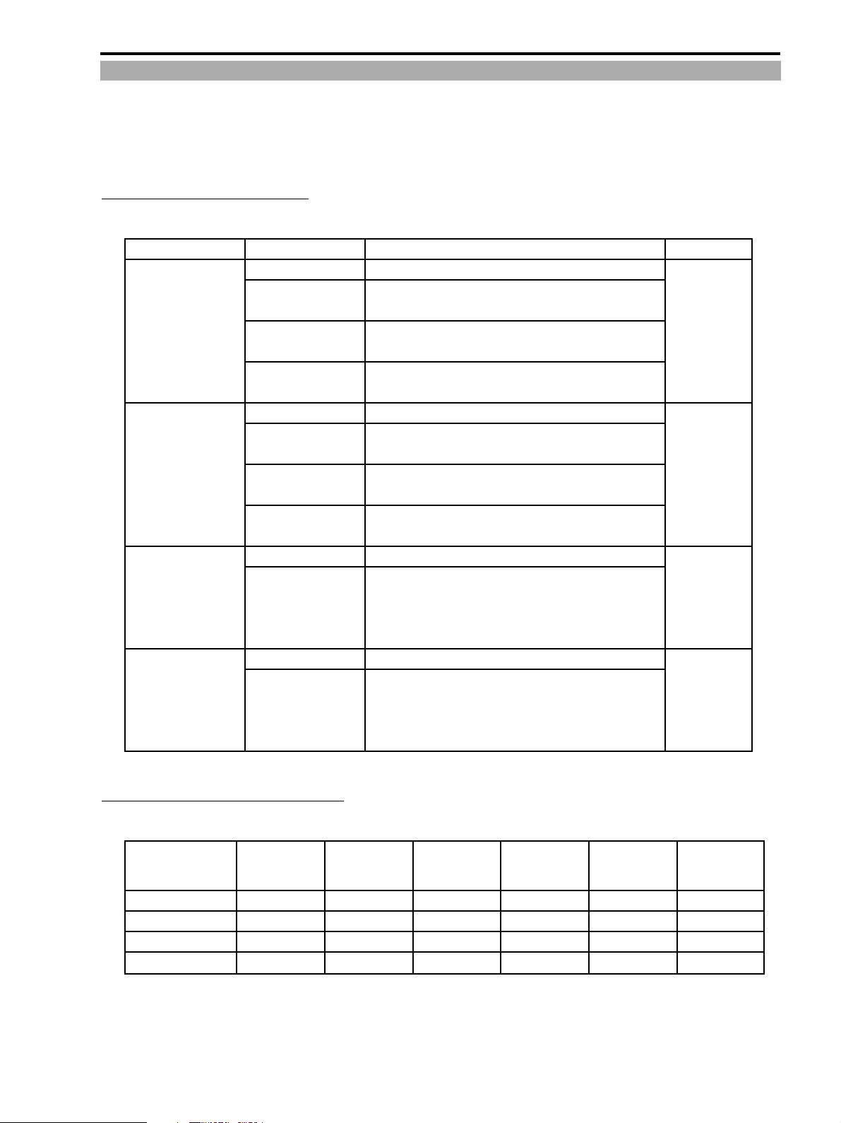
If an anomaly occurs in any of the rotation drive systems (drum, capstan, reel and loading), the specified error operations
in accordance with each mode is performed. The message “Please unload the cassette” appears on LCD and “EJECT”
blinks.
5-4-1 Error Detecting Conditions
The error detecting conditions in the following table.
Error type
Drum error
Capstan error
Reel error
Loading error
Condition
Error detecting mode
FG frequency during
normal operation
Error detection level
Error detection time
Error detecting mode
FG frequency during
normal operation
Error detection level
Error detection time
Error detecting mode
Error detection
Error detecting mode
Error detection
During Starting up/During normal operation
900Hz
During Starting up : Outside the range of 80% to 150%
During normal operation : 30% or less
During Starting up : 5 seconds
During normal operation : 0.5 seconds
During Starting up/During normal operation
1347Hz
During Starting up : 80% or less
During normal operation : 100 Hz or less
During Starting up : 2 seconds
During normal operation : 0.5 seconds
During normal operation/During unloading
During normal operation : Number of C-FG during one
cycle of reel FG is 2.4×1347 pulses or more.
During unloading : Half cycle of reel FG is 1 second or
longer (Both on take-up reel only)
During mode transition period
Mode transition time
STANDBY-STOP : 6sec
STBY-POPUP : 3sec
STOP-PLAY : 3sec
Detection
D-FG
C-FG
T, S-REEL FG
C-FG
MODE switch
5-4-2 Processing after Error Detection
Processing after error detection is shown in the following table.
Cassette in Loading During unloading Loaded end
Drum error Pop up Pop up Error stop Error stop Error stop Error stop
Capstan error Pop up ------- Error stop Error stop Error stop Error stop
Reel error ------- ------- Error stop Error stop Error stop Error stop
Loading error Pop up Pop up Error stop Error stop ------- Error stop
While tape is
running
• Pop up : Error display → error eject → pop up → error clear
• Error stop : Error display → STOP position (not cleared unless EJECT is performed)
2-17
While mode
transition is in
progress
Page 16
ZR10A
TECHNICAL DESCRIPTION
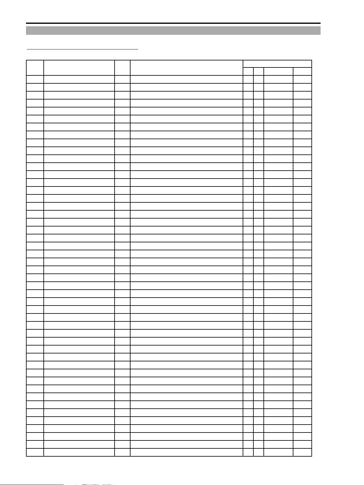
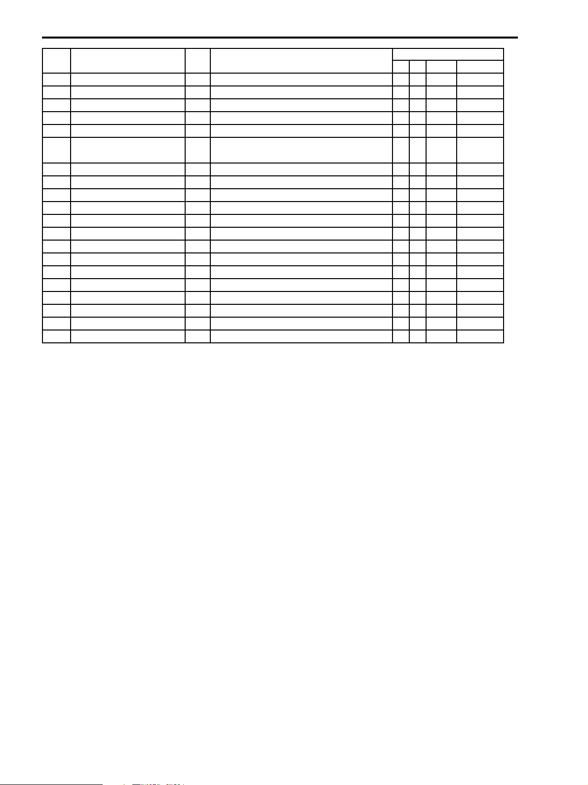
5-5 IC Terminal Functions
5-5-1 CAMERA Microcomputer (IC1401)
Pin Name I/O Function Remarks
PG BK ADDR Data Bit
3
AVCC
4
(PWM ZB)
7
CAM REQ
8
XD IC IRQ
11
MOD0
12
DIC XRST REQ
13
/OE
17
X EEP CS
18
X PC CS
23
X PWM CS
24
IVCC
27
31
BVCC
32
IRIS CL
33
35
F PSB
37
38
MOD2
40
41
44
45
47
ADJ CS
48
SDI2
51
SDO1
54
56
ZOOM KEY
57
I ENC
58
AVREFF
59
PVSS
60
(PWM FB)
61
FSCLK
62
64
IVSS
67
68
CAM PHOTO
70
71
X PC ACK
72
X EEP WP
73
IVCC/VPP1
74
X TG SEN
76
78
79
FID
80
CAM RX
82
BVSS
83
IRIS OP
84
AGC WRT
A/D power supply
O
(PWM output for zoom drive)
I
MAIN microcomputer communication REQ (Pull down)
I
DIC interrupt signal
I
Single/flash mode setting (Pull down)
O
DIC reset request signal (to MAIN)
O
Used in flash mode
O
Chip select for EEPROM (Pull up)
O
Chip select for AF debug
O
Chip select for PWM (to DIC)
Internal power supply
O
Not used (Open)
Port/bus power supply
O
Closing the iris forcibly
O
Not used (Open)
O
Focus power save
O
Not used (Open)
I
Operating mode setting (GND)
O
Not used (Open)
O
Not used (Open)
O
Not used (Open)
O
Not used (Open)
O
Chip select for factory adjustment
I
MAIN/FIC serial data reception
O
DIC serial data transmission
I
Not used (GND)
I
Zoom key
I
Iris encoder
A/D reference voltage
Port GND
O
(PWM for focus drive)
O
Used in flash mode
O
Not used (Open)
Internal GND
O
Not used (Open)
O
Timing signal to photo (to MAIN)
O
Not used (Open)
I/O
For AF debug/WB debug
O
EEPROM write protection (Pull down)
Internal power supply/flash program power supply
O
TG serial communication enable signal
O
Not used (Open)
O
Not used (Open)
I
Field index input (from DIC)
O
MAIN microcomputer send/receive discrimination signal
Port/bus GND
O
Opening the iris forcibly
O
AGC data write pulse signal
5
0
5
0
5
0
5
0
5
0
5
0
5
0
5
0
5
0
5
0
5
0
5
0
5
0
5
0
5
0
5
0
5
0
5
0
5
0
5
0
1DD0, 1DD1
5
0
5
0
5
0
5
0
5
0
5
0
5
0
5
0
5
0
5
0
5
0
5
0
07B6
07B1
07B1
0780
0780
0783
0783
0782
0781
0784
0784
07B4
07B4
07B5
07B5
07B2
07B2
07B3
1BB0
07B6
07B1
07B1
0780
0780
0783
0783
0783
0782
0782
0781
0781
4
3
1
6
3
5
2
1
7
1
5
2
5
2
5
7
4
3
6
6
4
5
2
6
3
0
6
0
4
1
2-18
Page 17

TECHNICAL DESCRIPTION
Pin Name I/O Function Remarks
PG BK ADDR Data Bit
85
86
88
89
90
91
92
93
94
95
96
97
101
102
103
104
105
106
107
108
111
112
113
114
115
116
117
118
119
120
122
123
124
125
126
127
128
131
132
133
134
135
136
139
140
141
142
143
144
146
147
148
LED RET
IRIS GAIN
PVSS
SCLK2
SDI0
AVSS
Y GYRO
PVCC
(PWM ZA)
FSDA
XOUT
/RESET
CAM SS TMG1
CG STB
ADJ SW
X PC REQ
ADJ REQ
BVCC
AGC CS
X TG RST
IVSS
NT XPL SEL
DA LOAD
IVCC/VPP2
X AGC RST
IVSS
IVCC
I ISW
EEP INI
DIC READ
SDO2
SCLK1
SCLK0
SDO0
P GYRO
(PWM FA)
FBUSY
O
Not used (Open)
O
Not used (Open)
O
Turning on the lens LED
O
Not used (Open)
O
Not used (Open)
O
Not used (Open)
O
Not used (Open)
O
Iris gain
O
Not used (Open)
O
Not used (Open)
Port GND
I/O
MAIN/TG/AGC/DA/FIC serial clock
I
Strobe/EEPROM serial data reception
A/D GND
I
Yaw direction gyro input
I
Not used (GND)
I
Not used (GND)
Port power supply
O
(PWM for zoom drive)
O
Used in flash mode
O
Main clock output
I
Used in reset/flash mode
O
Slow shutter timing signal (to SUB)
O
CG strobe output
I
For factory adjustment (Pull up)
I/O
For AF debug/WB debug
I
REQ signal for factory adjustment (Pull down)
Port/bus power supply
O
Chip select for AGC (pull)
O
TG reset signal
Internal GND
I
NTSC/PAL selection
O
D/A load pulse
O
Not used (Open)
Internal power supply/flash program power supply
O
AGC reset signal
O
Not used (Open)
O
Not used (Open)
Internal GND
Internal power supply
O
Gyro output personal computer charging switch
I
EEPROM initialization request (Pull up)
O
DIC data read
O
MAIN/TG/AGC/DA/FIC serial data transmission
O
DIC serial clock
O
EEPROM serial clock
O
EEPROM serial data transmission
I
Not used (GND)
I
Pitch direction gyro input
O
(PWM output for focus drive)
O
Used during flash mode
I
Not used (Open)
5
0
0784
5
0
0784
5
0
07B4
5
0
07B4
5
0
07B4
5
0
07B4
5
0
07B4
5
0
07B5
5
0
07B5
5
0
07B2
5
0
07B3
5
0
1F90, 1F91
5
0
07B6
5
0
07B1
5
0
0780
5
0
0780
5
0
0783
5
0
0783
5
0
0783
5
0
0782
5
0
0782
5
0
0781
5
0
0781
5
0
0781
5
0
0784
5
0
07B4
5
0
07B5
5
0
07B5
5
0
07B2
5
0
07B3
5
0
07B3
5
0
07B3
5
0
1F92, 1F93
5
0
07B6
5
0
07B1
5
0
07B1
ZR10A
0
6
0
1
3
6
7
4
7
5
1
5
7
7
4
7
4
1
7
4
6
3
0
7
4
3
6
3
5
2
0
7
5
2
2-19
Page 18
ZR10A
TECHNICAL DESCRIPTION
Pin Name I/O Function Remarks
PG BK ADDR Data Bit
149
150
151
152
154
156
157
158
160
161
163
164
165
166
169
170
172
173
174
176
/NMI
XIN
IVCC
MOD1
BVSS
X TG VEN
X DIC CS
X FIC CS
IVSS/VEE
Z PSB
F RES SW
Z RES SW
PVCC
CAM CS
X CCC
SDI1
I
Nonmaskable interrupt (Pull up)
I
Main clock input
Internal power supply
I
Single/flash mode setting (Pull down)
Port/bus GND
TG serial communication enable signal (for image
O
stabilization)
O
DIC chip select (to DIC)
O
FIC chip select (to DIC)
Internal GND/power for flash erase
O
Not used (Open)
O
Not used (Open)
O
Zoom power save
I
Focus reset detection switch (Pull down)
I
Zoom reset detection switch (Pull down)
Port power supply
O
SUB microcomputer communication chip select
O
Not used (Open)
O
Not used (Open)
I
DIC serial data reception
O
Not used (Open)
5
0
0782
5
0
0782
5
0
0782
5
0
0781
5
0
0781
5
0
0784
5
0
0784
5
0
0784
5
0
07B2
5
0
07B3
5
0
07B3
5
0
07B3
5
0
07B2
5
3
2
5
2
2
3
4
6
7
6
4
2
2-20
Page 19

TECHNICAL DESCRIPTION
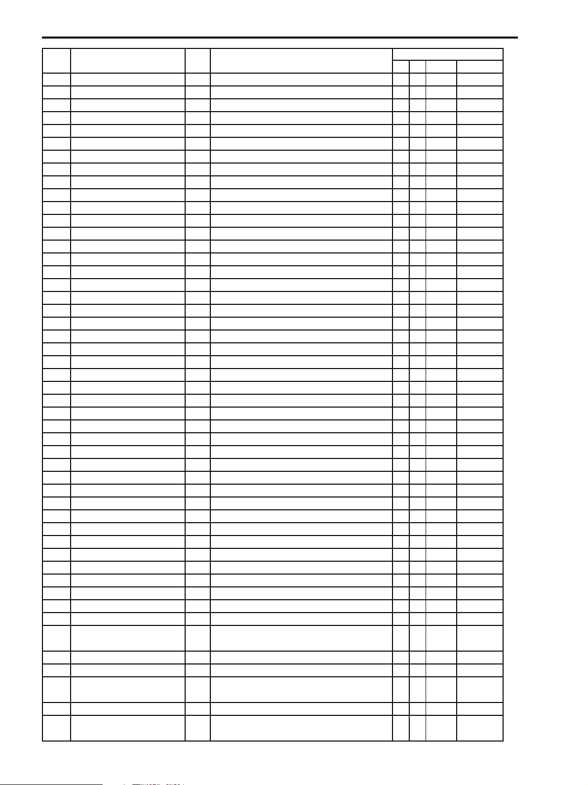
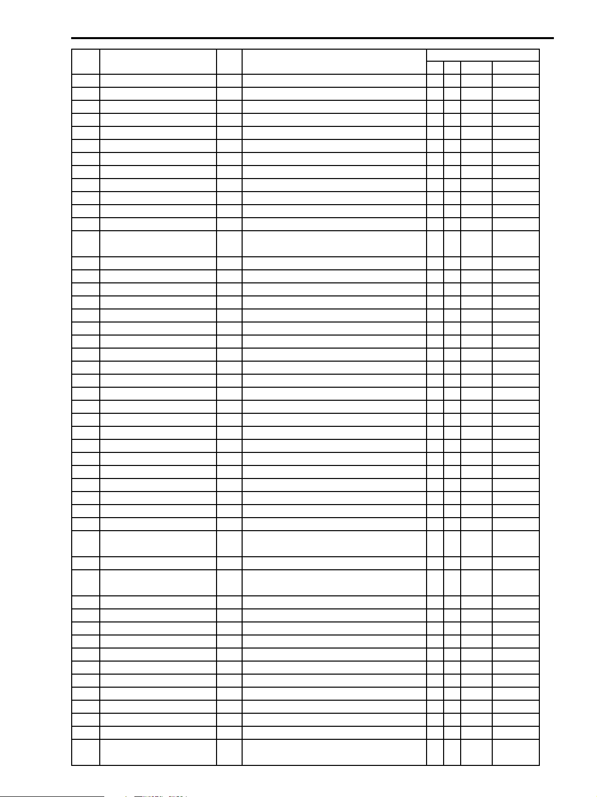
5-5-2 Main Microcomputer (IC100)
Pin Name I/O Function Remarks
PG BK ADDR Data Bit
VCC
1
2
3
4
5
6
7
8
9
10
11
12
13
14
15
16
17
18
19
20
21
22
23
24
25
26
27
28
29
30
31
32
33
34
35
36
37
38
39
40
41
42
43
44
45
46
47
48
49
50
VIF CS
XECSV
XECSI
OPT CS
VCCB
VSSB
MIRR
N.C
N.C
N.C
N.C
N.C
N.C
VCO HI
VCCB
VSSB
XRESET
EADDR6
EADDR5
EADDR4
EADDR3
EADDR2
EADDR1
EADDR0
EDATA15
EDATA14
EDATA13
EDATA12
EDATA11
EDATA10
EDATA9
EDATA8
VCCB
VSSB
EDATA7
EDATA6
EDATA5
EDATA4
EDATA3
EDATA2
EDATA1
EDATA0
VIC XERD
VIC XEWR
WIDE CONT
LINE IN
VCCB
BCLK
VSSB
DVDD 2.2V
O
VIF chip select
VIC2 (VIC CS) chip select
O
VIC2 (DIF CS) chip select
O
O
OPT chip select (for factory adjustment)
BUS power supply = DVDD3V
BUS GND
O
Panel OSD OFF during mirror mode
O
O
O
O
O
O
VRP VCO power save
O
Bus power supply = DVDD3V
Bus GND
VIC initial signal
O
Address bus (VIC2)
O
O
Address bus (VIC2)
Address bus (VIC2)
O
Address bus (VIC2)
O
O
Address bus (VIC2)
O
Address bus (VIC2)
Address bus LSB (VIC2)
O
I/O
Data bus MSB (VIC2)
I/O
Data bus (VIC2)
Data bus (VIC2)
I/O
I/O
Data bus (VIC2)
I/O
Data bus (VIC2)
Data bus (VIC2)
I/O
I/O
Data bus (VIC2)
I/O
Data bus (VIC2)
Bus power supply = DVDD3V
Bus GND
I/O
Data bus (VIC2)
Data bus (VIC2)
I/O
I/O
Data bus (VIC2)
I/O
Data bus (VIC2)
Data bus (VIC2)
I/O
I/O
Data bus (VIC2)
I/O
Data bus (VIC2)
Data bus LSB (VIC2)
I/O
O
VIC2
O
VIC2
S1 signal control output
O
O
LINE input circuit control
Bus power supply = DVDD3V
Check pad
O
GND
2
7
7
7
7
7
7
7
7
7
7
7
7
7
7
7
7
7
7
7
7
7
7
7
7
7
7
7
7
7
7
7
7
7
7
7
7
7
7
7
7
7
D7
2
D7
2
D7
2
D7
2
D2
2
D2
2
D2
2
D2
2
D2
2
D2
2
D2
2
D2
2
D3
2
D3
2
D3
2
D3
2
D3
2
D3
2
D3
2
D3
2
D4
2
D4
2
D4
2
D4
2
D4
2
D4
2
D4
2
D4
2
D5
2
D5
2
D5
2
D5
2
D5
2
D5
2
D5
2
D5
2
D6
2
D6
2
D6
2
D6
2
D6
ZR10A
3
2
1
0
7
6
5
4
3
2
1
0
7
6
5
4
3
2
1
0
7
6
5
4
3
2
1
0
7
6
5
4
3
2
1
0
3
2
1
4
0
2-21
Page 20
ZR10A
TECHNICAL DESCRIPTION
Pin Name I/O Function Remarks
PG BK ADDR Data Bit
VSS
51
CAM RX DATA
52
DIC2S FI
53
CAM SS TMG1
54
CAM SS TMG2
55
PHOTO SW
56
HALF PHOTO SW
57
START/STOP
58
PAE/GREEN SW
59
PANEL OPEN SW
60
PANEL BOTTOM/TOP SW
61
CASSETTE IN SW
62
REC PROOF SW
63
DIAL CW SW
64
DIAL CCW SW
65
VCCP
66
AIF CS
67
EXT CONT
68
VSSP
69
PD DA
70
PD AD
71
A MUTE
72
A EMP2
73
A EMP1
74
AUD ON
75
N.C
76
BUZZER CARRIER1
77
N.C
78
TEST1
79
EVF SENS
80
LANC IN
81
LANC OUT
82
EVF DA LOAD
83
AIF/VIF/SUB SCK
84
SUB SI
85
AIF/VIF/SUB SO
86
PANEL IC CS
87
VCCP
88
VSSP
89
PANEL EEPROM CS
90
MAIN EEPROM CS
91
OSDC/EEPROM/DA SCK
92
EEPROM SI
93
OSDC/EEPROM/DA CS
94
DIC2S I/F CONT
95
DIC2S CS
96
CAM/DIC2S SCK
97
CAM SI
98
CAM/DIC2S SO
99
GND
Camera communication data discrimination
I
DIC shrink FI (not used)
I
Camera still picture control 1 input
I
Camera still picture control 2 input
I
Memory switch full pressing detection input
I
Memory switch half pressing detection input
I
Trigger switch input
I
PAE mode select switch detection input
I
Panel open switch detection input
I
Panel BOTTOM/TOP switch detection input
I
CASSETTE IN switch detection input
I
Record inhibit switch detection input
I
Dial detection input
I
Dial detection input
I
DVDD3V
AIF2 chip select output
O
External microphone detection output
O
GND
Audio DA power save control
O
Audio AD power save control
O
Audio mute
O
Audio emphasis setting
O
Audio emphasis setting
O
Speaker/headphones power supply control
O
O
Buzzer 1 output
O
O
For factory adjustment
IC chip select for EVF drive
O
LANC data input
I
LANC data output
O
DA converter load for EVF
O
Serial clock (AIF/VIF/sub microcomputer)
I/O
Serial bus data input (sub microcomputer)
I
Serial bus data output (AIF/VIF/sub microcomputer)
O
LCD interface chip select output
O
DVDD3V
GND
LCD EEPROM chip select output
O
EEPROM chip select output
O
OSDC/EEPROM/LCD EEPROM/DA/EVFIC/LCDIC
O
Serial data input (EEPROM/LCD EEPROM)
I
OSCD/EEPROM/LCD EEPROM/DA/EVFIC/LCD I/F
O
chip select output
DIC2 shrink I/F control output
O
DIC2 shrink chip select output
O
Serial clock input (camera microcomputer/DIC2 shrink)
I
input
Serial data input (camera microcomputer)
I
Serial clock output (camera microcomputer/DIC2
O
shrink)
7
2
DD
7
2
DD
7
2
DD
7
2
DD
7
2
DE
7
2
DE
7
2
DE
7
2
DE
7
2
DE
7
2
DE
7
2
DE
7
2
DE
7
2
DF
7
2
DF
7
2
DB
7
2
DB
7
2
DB
7
2
DB
7
2
DB
7
2
DB
7
2
DB
7
2
DB
7
2
DA
7
2
DA
7
2
DA
7
2
DA
7
2
DA
7
2
DA
7
2
D9
7
2
D9
7
2
D9
7
2
D9
7
2
D9
7
2
D9
7
2
D9
7
2
D9
7
2
D8
7
2
D8
7
2
D8
7
2
D8
7
2
D8
7
2
D8
7
2
D8
7
2
D8
3
2
1
0
7
6
5
4
3
2
1
0
7
6
0
1
2
3
4
5
6
7
0
1
2
3
6
7
0
1
3
4
5
2
6
7
0
1
2
3
4
5
6
7
2-22
Page 21
TECHNICAL DESCRIPTION
Pin Name I/O Function Remarks
PG BK ADDR Data Bit
VCC
100
VCCP
101
EMULATOR
102
JTAG/EMULATOR/FLASH
103
JTAG/EMULATOR/FLASH
104
JTAG/EMULATOR/FLASH
105
EMULATOR
106
EMULATOR
107
EMULATOR
108
JTAG/EMULATOR/FLASH
109
JTAG/EMULATOR
110
VSSP
111
FLASH
112
GND
113
GND
114
MODE
115
EMULATOR/FLASH
116
VSS
117
REST IN
118
VSS
119
OSCVCC
120
XIN
121
OSCVSS
122
XOUT
123
PLLCVCC
124
PLLCAP
125
PLLVSS
126
OSDC CS
127
OSDC CS
128
VSSB
129
VCCB
130
PANEL XOE
131
EVF BACKLIGHT ON
132
PANEL LCK
133
FCHO
134
EVF PW ON
135
LI3V DETECT
136
CAM PW ON
137
DA CFG
138
LET CONT
139
VCCP
140
VSSP
141
N.C
142
XINT M
143
XINT D
144
XINT C
145
SUB REQ
146
SUB CS
147
CAM PDINH
148
DVDD2.2V
DVDD3V
I
10k pull up (FP) emulator (for factory adjustment)
O
FP (for factory adjustment)
I
10k pull up (for factory adjustment)
I
10k pull up (for factory adjustment)
O
FP (emulator) (for factory adjustment)
O
FP (emulator) (for factory adjustment)
O
FP (emulator) (for factory adjustment)
I
10k pull up (for factory adjustment)
I
10k pull down (for factory adjustment)
GND
I
10k pull down (This terminal is open in the mask
version.)
GND
GND
10k pull down (for factory adjustment)
10k pull down (for factory adjustment)
GND
Reset signal input
GND
I
20 MHz
O
20 MHz
External capacitor for PLL is connected to this terminal
GND
O
OSDC IC chip select output
O
OSDC reset output
GND
DVDD3V
O
Shift clock for data to LCD DA converter
O
EVF back-light control output
O
Latch clock for data to LCD DA converter
I
Factory process mode/soft debug terminal 0 (for factory
adjustment)
O
EVF power supply control output
I
Low voltage detection of lithium primary backup
battery
O
Camera power supply control
O
DA CFG (for factory adjustment)
O
S1 signal letter box output
DVDD3V
GND
I
I
VIC RP CAPTURE interrupt request input
I
VIC DIF interrupt request input
I
VIC SDRAM interrupt request input
O
Communication request input to sub microcomputer
I
Selection input from sub microprocessor
O
“H” output during recorder mode (Interlocks with
camera power supply)
D1
2
7
D1
2
7
D1
2
7
D1
2
7
D1
2
7
D0
2
7
D1
2
7
D0
2
7
D1
2
7
DA
2
7
DA
2
7
E1
2
7
DC
2
7
DC
2
7
DC
2
7
DC
2
7
DC
2
7
DC
2
7
2-23
ZR10A
0
1
2
3
4
0
5
1
6
5
4
4
7
6
5
4
3
2
Page 22
ZR10A
TECHNICAL DESCRIPTION
Pin Name I/O Function Remarks
PG BK ADDR Data Bit
149
N.C
150
VCC
151
VSS
152
DIC2S VD
153
DIC XSYSRST
154
CAM CS
155
CAM PHOTO
156
CAM REQ
157
VCCP
158
VSSP
159
N.C
160
HP DET
161
EXT DET
162
S DET
163
PLUG IN
164
N.C
165
LOAD
166
UNLOAD
167
ID REQ
168
LMO CONT
169
CAP ON
170
XIDACK
171
CAP FWD
172
TAPE LED
173
N.C
174
DRUM ON
175
SELCSLP
176
REEL LED CONT
177
XCIN
178
VSSR
179
XCOUT
180
VCCR
181
AVREF
182
AVCC
183
DEWDETECT
184
KEY AD0
185
KEY AD1
186
KEY AD2
187
KEY AD3
188
KEY AD4
189
S REEL FG
190
T REEL FG
191
TAPE TOP AD
192
TAPE END AD
193
MSW AD
194
RAGC
195
WIDE DET
196
N.C
197
N.C
198
N.C
199
AVSS
O
DVDD2.2V
GND
[Interrupt] DIC2 shrink VD input
I
DIC/FIC reset output
O
[Interrupt] camera microprocessor chip select input
I
Timing signal input for photo
I
Camera microprocessor communication request output
O
DVDD3V
GND
O
Headphones jack detection input
I
External microprocessor detection input
I
S-terminal connection detection
I
AV multi-terminal insertion detection
I
I
Loading motor control (LOAD)
O
Loading motor control (UNLOAD)
O
N.C. (for development investigation)
I
Loading motor control (CONT)
O
Capstan motor start/stop signal output
O
N.C. (for development investigation)
O
Capstan motor rotation direction signal output
O
Tape LED illuminant control
O
O
Drum motor start/stop signal output
O
Drum driver control
O
Reel sensor LED illumination power save
O
32 kHz
I
32 kHz
O
Power flag is set when VCCR decreases to 0.1 V or less
once then increases back to 1.8 V.
DVDD3V
DVDD3V
Dew condensation detection
I
Operation key detection (DE ON/OFF, DE, MENU)
I
Operation key detection (PLAY, FF)
I
Operation key detection (STOP, REW)
I
Operation key detection (EXECUTE)
I
Operation key detection (Unused)
I
S-reel FG signal input
I
T-reel FG signal input
I
Tape top sensor signal input
I
Tape end sensor signal input
I
Mechanism mode detection
I
VRP AGC signal detection
I
S1 signal voltage detection (wide signal detection)
I
I
I
I
GND
7
2
DC
7
2
DC
7
2
DD
7
2
DD
7
2
DD
7
2
DD
7
2
DF
7
2
DF
7
2
DF
7
2
DF
7
2
DF
7
2
DF
7
2
E0
7
2
E0
7
2
E1
7
2
E0
7
2
E0
7
2
E1
7
2
E0
7
2
E0
7
2
E1
7
2
E0
7
2
E1
7
2
E0
7
2
C0
7
2
C1
7
2
C2
7
2
C3
7
2
C4
7
2
C5
7
2
C6
7
2
C7
7
2
C8
7
2
C9
7
2
CA
7
2
CB
7
2
CC
7
2
CD
7
2
CE
7
2
CF
1
0
7
6
5
4
5
4
3
2
1
0
7
6
3
5
4
2
3
2
1
1
0
0
2-24
Page 23

TECHNICAL DESCRIPTION
5-5-3 Sub Microcomputer (IC203)
Pin Name I/O Function Remarks
PG BK ADDR Data Bit
SUB CS
1
RMC PULSE IN
2
SUB REQ
3
E3V DETECT
4
N.C
5
LANC PW CONT
6
SCLK2
7
SIN2
8
SOUT2
9
MIC SCL
10
MIC SDA
11
CNVSS
12
XCIN
13
XCOUT
14
RESET
15
XIN
16
XOUT
17
VSS
18
DC J DET
19
CAS IN
20
EJECT SW
21
LANC ON
22
N.C
23
N.C
24
CAM PW SW
25
VTR PW SW
26
VTR PW LED
27
CAM PW LED
28
TALLY LED
29
MIC ON
30
PS
31
CHG CLK
32
CHG DATA
33
CHG CS
34
F CH
35
SERVICE M S
36
MIC3
37
MIC2
38
MIC1
39
D OUT
40
BATT INFO AD
41
BATT AD
42
VCC
43
VREF
44
AVSS
45
CHGLED2
46
N.C
47
VTR ON
48
O
Sub microcomputer communication enable signal
I
[Interrupt] input signal from remote controller
I
[Interrupt] main microcomputer communication request
input
I
[Interrupt] E3V low voltage detection input
O
O
LANC power supply control output
O
Sub microprocessor serial clock output
O
Sub microprocessor serial data output
I
Sub microprocessor serial data input
O
Cassette memory communication clock output terminal
I/O
Cassette memory communication data terminal
GND
I
Sub clock input
O
Sub clock output
I
Reset signal input
I
Main clock input
O
Main clock output
GND
I
DC jack insertion detection (Detection by voltage)
I
CASSETTE IN switch detection
I
EJECT switch detection
I
LANC power ON detection
I
I
I
Camera mode, POWER switch detection
I
VTR mode, POWER switch detection
O
VTR mode, POWER LED control
O
Camera mode, POWER LED control
O
Tally LED control
O
Cassette memory, power supply control
O
Power save
O
Charger IC, serial clock
O
Charger IC, serial data
O
Charger IC, chip select
I
Function check (for factory adjustment)
I
Main serial is not detected. (for factory adjustment)
I
Cassette memory/ID board detection
I
Cassette memory/ID board detection
I
Cassette memory/ID board detection
I
Charging current and voltage detection
I
Battery type detection
I
Battery low voltage detection
E3V + L13V
E3V
GND
O
Charger LED2
O
O
VTR power supply control
3
7
7
7
7
7
7
7
7
7
7
7
7
7
7
7
7
7
7
7
7
7
7
7
7
7
7
7
7
7
7
7
7
7
7
7
7
7
7
7
7
FC
3
FC
3
FC
3
FC
3
FC
3
FA
3
FA
3
FA
3
FA
3
FA
3
FA
3
FA
3
FA
3
F9
3
F9
3
F9
3
F9
3
F9
3
F9
3
F9
3
F9
3
F8
3
F8
3
F8
3
F8
3
F8
3
F8
3
F8
3
F8
3
F7
3
F6
3
F5
3
F4
3
F3
3
F2
3
F1
3
F0
3
FC
3
FC
3
FC
ZR10A
4
3
2
1
0
3
2
1
0
3
2
1
0
7
6
5
4
3
2
1
0
7
6
5
4
3
2
1
0
7
6
5
2-25
 Loading...