

Page 1

Device handbook
APLUS-LED
Operating Instructions APLUS with LED display or without display
157 679-19 (PM 1000357 000 01) 04/2016
Camille Bauer Metrawatt AG
Aargauerstr asse 7
CH-5610 Wohlen / Switzerland
Phone: +41 56 618 21 11
Telefax: +41 56 618 35 35
e-Mail: info@cbmag.com
http://www.camillebauer.com
Page 2

2/89 Device handbook APLUS with / without LED display, 157 679-19, 04/2016
Legal information
Warning notices
In this document warning notices are used, which you have to observe to ensure personal safety and to prevent
damage to property. Depending on the degree of danger the following symbols are used:
If the warning notice is not followed death or severe personal injury
will result.
If the warning notice is not followed damage to property or severe
personal injury may result.
If the warning notice is not followed the device may be damaged or
may not fulfill the expected functionality.
Qualified personnel
The product described in this document may be handled by personnel only, which is qualified for the respective
task. Qualified personnel have the training and experience to identify risks and potential hazards when working
with the product. Qualified personn el are als o able to understa nd and follow the given safety and warning
notices.
Intended use
The product described in this document may be used only for the application specified. The maximum electrical
supply data and ambient conditions specified in the technical data section must be adhered. For the perfect and
safe operation of the device proper transport and storage as well as professional assembly, installation,
handling and maintenance are required.
Disclaimer of liability
The content of this document has been reviewed to ensure correctness. Nevertheless it may contain errors or
inconsistencies and we cannot guarantee completeness and correctness. This is especially true for different
language versions of this document. This document is regularly reviewed and updated. Necessary corrections
will be included in subsequent version and are available via our webpage http://www.camillebauer.com
.
Feedback
If you detect errors in this document or if there is necessary information missing, please inform us via e-mail to:
customer-support@camillebauer.com
Page 3

3/89 Device handbook APLUS with / without LED display, 157 679-19, 04/2016
Contents
1. Introduction ..................................................................................................................... 5
1.1 Purpose of this document ........................................................................................................ 5
1.2 Scope of supply ....................................................................................................................... 5
1.3 Further documents .................................................................................................................. 5
2. Security notes .................................................................................................................. 6
3. Device overview............................................................................................................... 6
3.1 Brief description ....................................................................................................................... 6
3.2 Possible modes of operation ................................................................................................... 7
3.3 Monitoring and alarming .......................................................................................................... 8
3.3.1 Alarming concept ................................................................................................................................. 8
3.3.2 Logic components ..............................................................................................................................10
3.3.3 Limit values ........................................................................................................................................11
3.3.4 Sequence of evaluation .....................................................................................................................12
3.4 Free Modbus image .............................................................................................................. 13
4. Mechanical mounting .................................................................................................... 14
4.1 Panel cutout .......................................................................................................................... 14
4.2 Mounting of the device .......................................................................................................... 14
4.3 Demounting of the device ...................................................................................................... 14
5. Electrical connections .................................................................................................. 15
5.1 General safety notes ............................................................................................................. 15
5.2 Electrical connections of the I/Os .......................................................................................... 16
5.3 Possible cross sections and tightening torques ..................................................................... 16
5.4 Inputs .................................................................................................................................... 17
5.5 Rogowski current inputs ........................................................................................................ 21
5.6 Power supply ......................................................................................................................... 22
5.7 Relays ................................................................................................................................... 22
5.8 Digital inputs and outputs ...................................................................................................... 23
5.9 Analog outputs ...................................................................................................................... 25
5.10 Modbus interface RS485 X4 and / or X8 ............................................................................... 25
5.11 Profibus DP interface............................................................................................................ 26
6. Commissioning.............................................................................................................. 27
6.1 Software installation CB-Manager ......................................................................................... 27
6.2 Parametrization of the device functionality ............................................................................. 28
6.3 Installation check ................................................................................................................... 29
6.4 Installation of Ethernet devices .............................................................................................. 30
6.4.1 Connection ......................................................................................................................................30
6.4.2 Network installation using the CB-Manager software .....................................................................31
6.4.3 Network installation by means of local programming .....................................................................32
6.4.4 Time synchronization via NTP-protocol ..........................................................................................33
6.4.5 TCP ports for data transmission .....................................................................................................33
6.5 Installation of Profibus DP devices ........................................................................................ 34
6.6 Protection against device data changing ............................................................................... 35
7. Operating the device ..................................................................................................... 36
7.1 Display and operating elements ............................................................................................ 36
7.2 Operating modes ................................................................................................................... 37
7.3 Setting the display brightness ................................................................................................ 38
7.4 Display modes ....................................................................................................................... 39
7.5 Meter reading ........................................................................................................................ 42
Page 4

4/89 Device handbook APLUS with / without LED display, 157 679-19, 04/2016
7.6 Alarm handling ...................................................................................................................... 43
7.6.1 Alarm state display on the device ..................................................................................................... 43
7.6.2 Display of alarm texts ........................................................................................................................ 43
7.6.3 Acknowledgment of alarms via display ............................................................................................. 44
7.7 Resetting of measurements .................................................................................................. 45
7.8 Configuration ........................................................................................................................ 46
7.8.1 Selection of the parameter to edit ..................................................................................................... 50
7.8.2 Discrete selection .............................................................................................................................. 51
7.8.3 Setting value ..................................................................................................................................... 51
7.9 Data logger ........................................................................................................................... 52
7.9.1 Activation of data logger recording ................................................................................................... 52
7.9.2 SD card ............................................................................................................................................. 52
7.9.3 Access to logger data ....................................................................................................................... 53
7.9.4 Logger data analysis ......................................................................................................................... 53
8. Service, maintenance and disposal ............................................................................. 54
8.1 Protection of data integrity .................................................................................................... 54
8.2 Calibration and new adjustment ............................................................................................ 54
8.3 Cleaning................................................................................................................................ 54
8.4 Battery .................................................................................................................................. 54
8.5 Disposal ................................................................................................................................ 54
9. Technical data ................................................................................................................ 55
10. Dimensional drawings ................................................................................................... 60
Annex ................................................................................................................................... 62
A Description of measured quantities ............................................................................. 62
A1 Basic measurements............................................................................................................. 62
A2 Harmonic analysis ................................................................................................................. 65
A3 System imbalance ................................................................................................................. 66
A4 Reactive power ..................................................................................................................... 67
A5 Mean values and trend .......................................................................................................... 69
A6 Meters ................................................................................................................................... 70
B Dis pl ay matrices in FULL mode ................................................................................... 71
B0 Used abbreviations for the measurements ............................................................................ 71
B1 Display matrix single phase system ...................................................................................... 78
B2 Display matrix Split-phase (two-phase) systems ................................................................... 79
B3 Display matrix 3-wire system, balanced load ......................................................................... 80
B4 Display matrix 3-wire systems, unbalanced load ................................................................... 81
B5 Display matrix 3-wire systems, unbalanced load, Aron .......................................................... 82
B6 Display matrix 4-wire system, balanced load ......................................................................... 83
B7 Display matrix 4-wire systems, unbalanced load ................................................................... 84
B8 Display matrix 4-wire system, unbalanced load, Open-Y ....................................................... 85
B9 Display matrix of mean-values of power quantities ................................................................ 86
C FCC statement ............................................................................................................... 87
INDEX ................................................................................................................................... 88
Page 5

5/89 Device handbook APLUS with / without LED display, 157 679-19, 04/2016
1. Introduction
1.1 Purpose of this document
This document describes the universal measurement device for heavy-current quantities APLUS. It is
intended to be used by:
• Installation personnel and commissioning engineers
• Service and maintenance personnel
• Planners
Scope
This handbook is valid for all hardware versions of the A
PLUS with LED display or without display. Some of
the functions described in this document are available only, if the necessary optional components are
included in the device.
Required knowledge
A general knowledge in the field of electrical engineering is required. For assembly and installation of the
device knowledge of applicable national safety regulations and installation standard is required.
1.2 Scope of supply
• Measurement device APLUS
• Safety instruct ions (multiple languages)
• Connection set basic unit: Plug-in terminals and mounting clamps
• Optional: Connection set I/O extension: Plug-in terminals
1.3 Further documents
Via our homepage http://www.camillebauer.com further documents about the APLUS can be downloaded:
• Safety instructions APLUS
• Data sheet A
PLUS
• Modbus basics: General description of the communication protocol
• Modbus interface A
PLUS: Register descript ion of Modbus/RTU communication via RS-485
• Modbus/TCP interface A
PLUS: Register description of Modbus/TCP communication via Ethernet
Page 6

6/89 Device handbook APLUS with / without LED display, 157 679-19, 04/2016
2. Security notes
Device may only be disposed in a professional manner !
The installation and commissioning should only be carried out by trained personnel.
Check the following points before commissioning:
– that the maximum values for all the connections are not exceeded, see "Technical data"
section,
– that the connection wires are not damaged, and that they are not live during wiring,
– that the power flow direction and the phase rotation are correct.
The instrument must be taken out of service if safe operation is no longer possible (e.g. visible
damage). In this case, all the connections must be switched off. The instrument must be
returned to the factory or to an authorized service dealer.
It is forbidden to open the housing and to make modifications to the instrument. The instrument
is not equipped with an integrated circuit breaker. During installation check that a labeled switch
is installed and that it can easily be reached by the operators.
Unauthorized repair or alteration of the unit invalidates the warranty.
3. Device overview
3.1 Brief description
The APLUS is a comprehens ive instrument for the u niversal measurem ent, monitoring and power quality
analysis in power systems. The device can be adapted fast and easily to the meas urement task by means
of the CB-Manager software. T he universal measurement s ystem of the device may be used directl y for
any power system , from single ph ase up to 4-wire unbalanced netw orks, without hardware m odifications.
Independent of measurement task and outer influences always the same high performance is achieved.
Using additional, opt ional com ponents the opportunities of the A
PLUS m ay be extended . You may choose
from I/O extens ions, communic ation interf aces or data log ger. The nam eplate on the d evice gives f urther
details about the present version.
The version with top-ha t rail adapter instead of the display has th e same dimens ions and connec tions as
the version with display and supports the same options.
Page 7

7/89 Device handbook APLUS with / without LED display, 157 679-19, 04/2016
3.2 Possible modes of operation
The APLUS can cover a wide range of possible input ranges without any hardware variance. The adaption
to the input signal is performed by means of variable amplifying levels for current and voltage inputs.
Depending on the application it makes sense to fix these levels by means of the configuration or to let
them stay variable to achieve a maximum accuracy during measurement. The differentiation, if the
amplifying remains constant or is adapted to the present value, is done during the definition of the input
configuration by means of the parameter "auto-scaling".
The disadvantage of auto-scaling is t hat whe n an amplifying level needs to be changed, a settling time of
at least one cycle of the power frequency must be allowed until the signals have stabilized again. During
this short time the measurement results remain frozen.
Continuous measurement
An absolute uninterrupted measurement of all quantities assumes that auto-scaling is deactivated for both
voltage and current inputs.
Metering
The uncertainty of the active energy meters of the A
PLUS is given with class 0.5S. To fulfill the high
requirements of the underlying meter standard EN 62053-22 also small currents have to be measured
very accurate. To do so, auto-scaling must be activated for current inputs. For metering applications the
system voltage is assumed to be quite constant, nominal value acc. standard, wherefore auto-scaling for
voltages is not required. The subsequent example shows an appropriate configuration, which also
conforms to the factory setting of the device.
Dynamic monitoring of limit values
An important criterion when monitoring the quality of the supply voltage is the possibility to detect short
sags of the system voltage. To be able to follow the progress of the voltage auto-scaling of the voltage
inputs should be deactivated. Thereby you have to consider that a possible swell of the voltage may be
detected only up to the configured overriding (20% of rated voltage in the above example), because the
switching of the measurement range is locked in both directions.
This applies analogously to all quantities of the system, whose progress should be monitored. For power
quantities the voltage amplification as well as the current amplification is influenced. However, which basic
quantities may vary how much can differ from application to application.
Page 8

8/89 Device handbook APLUS with / without LED display, 157 679-19, 04/2016
3.3 Monitoring and alarming
The logic module integrated in the APLUS is a powerful feature to monitor critical situations without delay
on device side. By implementing this local intelligence a safe monitoring can be realized which is
independent of the readiness of the control system.
3.3.1 Alarming concept
How alarms are handled is decided during the configuration of the device. For that in the logic module you
can define if LED's are used for alarm state display and how resp. when a possibly activated action, such
as the switching of a relay, will be reset. These configuration parameters are highlighted in yellow in the
following chart.
LED ON
Alarm
acknowledged
?
Alarm state
still persists ?
slow flashing
Y
Y
Y
N
N
Acknowledg.
of LEDS
required ?
Stop
flashing
LED OFF
Alarm state
still persists ?
N
Y
N
Fast
flashing
ALARM
LED used
for alarm
display ?
No action
N
Action
configurated
?
Perform action
Alarm state
still persists ?
Y
N
Action
resettable
?
Reset
?
Action reset
Y
N
N
Y
N
Y
Y
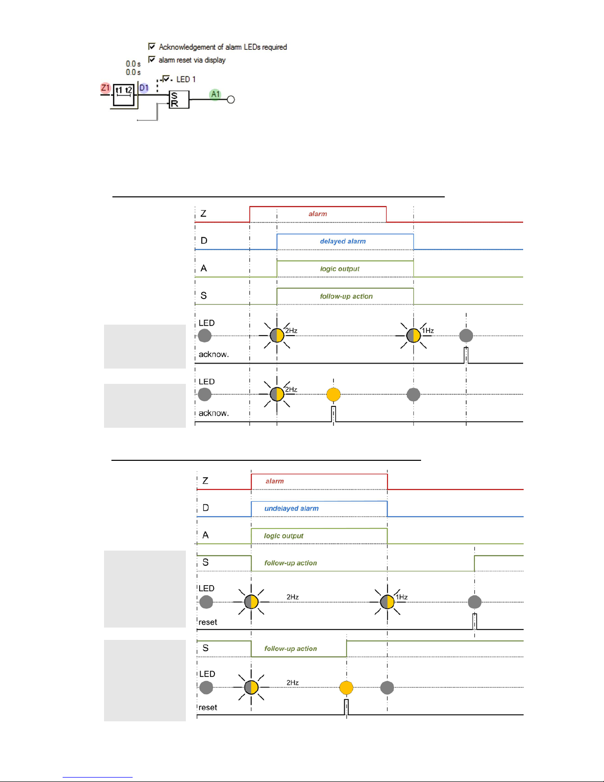
► Acknowledgment: This procedure affects the state of the LED only
If an alarm state is visualized via LED, its occurence must be acknowledged v ia displ a y (see:
Acknowledgment of alarms via display), no matter if it is still active (fast flashing) or has dropped-out
already (slow flashing). By acknowledging an alarm, only the flashing of the LED stops, but a reset of the
alarm action is performed only if the display is configured as a possible source for alarm reset.
Acknowledgment is not required if "acknowledgement of alarm LEDs required" in the
logic module configuration is not selected.
► Alarm reset : This procedure affects the states of the follow-up action and the LEDs
If an alarm state occurs a follow-up action (e.g. the switching of a relay) can be triggered. This follow-up
action is normally reset as soon as the alarm condition no longer exists. But the alarm handling may be
configured as well in a way that only by means of an alarm reset the subsequ ent o perati on is withdra w n.
This way an alarm remains stored until a reset is performed, even if the alarm situation no longer exists.
Possible sources for an alarm reset are the display, a digital input, another logical state of the logic
module or a command via the bus interface.
Hint: If an alarm is reset, the alarm state visualized via LED is acknowledged at the same time.
On the next page some signal flow examples are shown.
Page 9
9/89 Device handbook APLUS with / without LED display, 157 679-19, 04/2016
Z: Logic output determined from all involved logic
inputs
D: Corresponds to signal Z, delayed by the switch-in
resp. dropout delay
A: Output signal of the logic function
S: State of the subsequent operation (e.g. of a relay),
corresponds normally to A, but may be inverted
(subsequent operation: relay OFF)
1) Alarm reset inactive, switch-in and dropout delay 3s, follow-up action not inverted
Acknowledgment of
LED, inactive alarm
Acknowledgment of
LED, active alarm
2) Alarm reset active, switch-in and dropout delay 0s, follow-up action inverted
Reset when alarm is
inactive
Reset when alarm is
still active
Page 10
10/89 Device handbook APLUS with / without LED display, 157 679-19, 04/2016
3.3.2 Logic components
The logic outputs are calculated via a two level logical combination of states, which are present at the
inputs. Usable components are AND, OR and XOR gates as well as their inversions NAND, NOR and
XNOR.
The principal function of the logical gates is given in the following table, for simplicity shown for gates with
two inputs only.
function symbol
older symbols
truth table plain text
ANSI 91-1984
DIN 40700 (alt)
AND
A B Y 0 0
0
0 1 0
1 0 0 1 1
1
Function is true if all input
conditions are fulfilled
NAND
A B Y
0 0 1
0 1 1 1 0 1 1 1 0
Function is true if at least
one of the input
conditions is not fulfilled
OR
A B Y
0 0 0 0 1 1 1 0 1 1 1
1
Function is true if at least
one of the input
conditions is fulfilled
NOR
A B Y 0 0 1 0 1 0 1 0
0
1 1 0
Function is true if none of
the input conditions is
fulfilled
XOR
A B Y
0 0 0
0 1 1
1 0 1
1 1 0
Function is true if exactly
one of the input
conditions is fulfilled
XNOR
A B Y
0 0 1
0 1 0
1 0 0 1 1
1
Function is true if all of
the input conditions are
fulfilled or all conditions
are not fulfilled
The logic components of the first level may combine up to three, the components of the second level up to
four input conditions. If individual inputs are not used, their state is automatically set to a condition which
has no influence on the logic result.
Page 11
11/89 Device handbook APLUS with / without LED display, 157 679-19, 04/2016
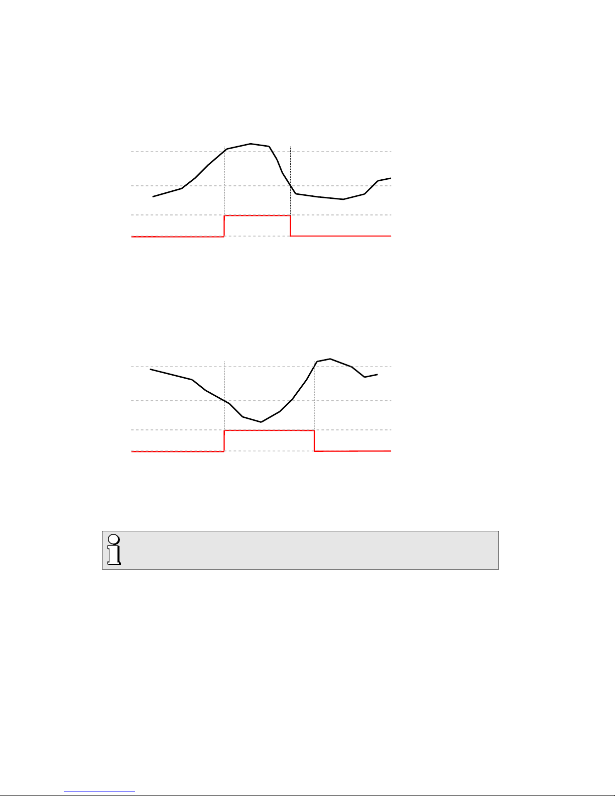
3.3.3 Limit values
States of limit values are the most important input quantities of the logic module. Depending on the
application, limits either monitor the exceeding of a given value (upper limit) or the fall below a given value
(lower limit). Limits are defined by means of two parameters, the limit for the ON and the limit for the OFF
state. The hysteresis is the difference between these two values.
Upper limit: The limit for ON state (
L.On
) is higher than the limit for the OFF state (
L.OFF
)
Limit for OFF state
Limit state
0
1
Limit for ON state
► The state 1 (true) results if the limit for ON state is exceeded. It remains until the value falls below the
limit for OFF state again.
► The state 0 (false) results if the limit for ON state is not yet reached or if, following the activation of the
limit value, the value falls below the limit for OFF state again.
Lower limit: The limit for ON state (
L.On
) is smaller than the limit for OFF state (
L.OFF
)
Limit for ON state
Limit state
0
1
Limit for OFF state
► The state 1 (true) results if the value falls below the limit for ON state. It remains until the value
exceeds the limit for OFF state again.
► The state 0 (false) results if the value is higher than the limit for ON state or if, following the activation
of the limit value, the value exceeds the limit for OFF state again.
If for a limit value the limit for ON state and the limit for OFF state are configured to
the same value, it will be treated as an upper limit value with a hysteresis of 0%.
Limit values may be used to control the running of operating hour counters. As long as the limit values
are fulfilled (logical 1) the operating hour counters keep on running. Not only operating times may be
measured, but e.g. time under overload condition (additional stress) as well.
Page 12

12/89 Device handbook APLUS with / without LED display, 157 679-19, 04/2016
3.3.4 Sequence of evaluation
The evaluation of the logic module is performed from top to bottom and from left to right:
1. Y1, Y2, Y3, Y4
2. Z1, Z2, Z3, Z4
3. D1, D2, D3, D4
4. A1, A2, A3, A4
► The evaluation is performed once each cycle of the power frequency, e.g. every 20ms at 50Hz. But the
time between two evaluations will never be longer than 25ms.
► If the logical states Y1...Y4, Z1...Z4, D1...D4 and A 1...A 4 are used as inputs, their changed states will
be included in the evaluation of the next interval
► Exception: In the first evaluation level the state of previous logical functions may be used as input
without delay, e.g. the state Y1 for the logical functions with output Y2, Y3 or Y4.
Page 13

13/89 Device handbook APLUS with / without LED display, 157 679-19, 04/2016
3.4 Free Modbus image
Accessing measured data of a Modbus device often needs some special effort, if the interesting
measurements are stored in different, non continuous register areas. This way multiple telegrams must be
sent to the device to read all data. This needs time and it's very likely, that the measurements don't
originate from the same measurement cycle.
A free assembly of the data to read helps a lot. The A
PLUS supports, along with the still available classical
Modbus image with thousands of registers, the facility to assemble two different images, which may be
read with one telegram only. These freely assembled images are refreshed after each measurement cycle
and therefore always provide the most present values.
The free float image
Up to 60 instantaneous, mean, unbalance or THD/TDD values may be arranged in any sequence on the
register addresses 41840-41958. All of these values are floating point numbers, which allocate 2 registers
per value. Meter values are not possible because they have another format.
The free integer image
Some older control systems are not able to handle float values. To make it possible to work with the data
of the device up to 20 16-Bit integer values can be derived from the existing measurement values. These
values will then be stored in the free Modbus image (register 41800 up to 41819) as integer values with
selectable range of values.
Example: Current transformer 100/5A, measurement current phase 1, over range 20%
► The reference value is 120A (maximum measurable current)
► The integer value shall be 12'000 if the measurement is 120A
After selecting the measured quantity and entering the register va lue of 12'000 automatically a scaling
factor of 100.0 is calculated. The measurement I1 therefore will be multiplied by 100.0 before it is
converted into an integer value and stored in the Modbus image.
Also in the integer image instantaneous, mean, unbalance or THD/TDD values may be arranged.
For devices with Profibus interface the Modbus image is used for the assembly of the
cyclical telegram. Via Modbus the same image can be used, but it’s not possible to use it
independently.
The Modbus communication of the A
PLUS is described in a separate document. Depending on the
communication hardware selected, either the manual for Modbus/RTU or Modbus/TCP protocol should be
used. These documents can be downloaded via our homepage http://www.camillebauer.com
.
► W157 695: Modbus/RTU interface APLUS (communication interface RS485)
► W162 636: Modbus/TCP interface A
PLUS (communication interface Ethernet)
Page 14

14/89 Device handbook APLUS with / without LED display, 157 679-19, 04/2016
4. Mechanic al mounting
► The standard version of the APLUS is designed for panel mounting as shown below
► The version without display with top-hat rail adapter may be clipped onto a top-hat rail according to
EN50022
Please ensure that the operating temperature limits are not exceeded when
determining the place of mounting (place of measurement):
-10 ... 55°C
4.1 Panel cutout
Dimensional drawing A
PLUS:
See section 10
4.2 Mounting of the device
The APLUS is suitable for panel widths up to 10mm.
a) Slide the device into the cutout from
the outside
b) From the side slide in th e m ounting
clamps into the intended openings and
pull them back about 2 mm
c) Tighten the fixation screws until the
device is tightly fixed with the panel
4.3 Demounting of the device
The demounting of the device may be performed only if all connected wires are out of service. Remove
all plug-in terminals and all connections of the current and voltage inputs . Pay attention to the fact, that
current transformers must be shortened before removing the current connections to the device. Then
demount the device in the opposite order of mounting (4.2).
Page 15

15/89 Device handbook APLUS with / without LED display, 157 679-19, 04/2016
5. Electrical connections
Ensure under all circumstances that the leads are free of potential
when connecting them !
5.1 General safety notes
Please observe that the data on the type plate must be adhered to !
The national provisions (e.g. in Germany VDE 0100 “Conditions concerning the erection of heavy
current facilities with rated voltages below 1000 V”) have to be observed in the installation and material
selection of electric lines!
Nameplate of a
device equipped
with RS485
interface and I/O
extension 1
Symbol Meaning
Device may only be disposed of in a professional manner!
Double insulation, device of protection class 2
CE conformity mark. The device fulfills the requirements of the applicable EU
directives.
Products with this mark comply with both the Canadian (CSA) and the American (UL)
requirements.
Caution! General hazard point. Read the operating instructions.
General symbol: Input
General symbol: Output
CAT III Measurement category CAT III for current / voltage inputs and power supply
CAT II
Measurement category CAT II for relay outputs
Page 16

16/89 Device handbook APLUS with / without LED display, 157 679-19, 04/2016
5.2 Electrical connections of the I/Os
I/O no. Terminal No. APLUS I/O extension 1 I/O extension 2
1 X2 1, 2, 3 Relay
2 X3 1, 2 Digital input
3 X3 3, 4 Digital output
4 X5 1, 2, 3 Relay Relay
5 X6 1, 2, 3 Relay
Relay
6 X7 1, 2 Digital I/O Digital I/O
7 X7 3, 4 Digital I/O Digital I/O
8 X7 5, 6 Analog output ±20mA Digital I/O
9 X7 7, 8 Analog output ±20mA Digital I/O
10 X7 9, 10 Analog output ±20mA Digital I/O
11 X7 11, 12 Analog output ±20mA Digital I/O
I/O no. -
as used in the CB-Manager software
5.3 Possible cross sectio n s and tightening torques
Inputs L1, L2, L3, N, I1 k-l, I2 k-l, I3 k-l
Single wire
1 x 0,5 ... 4,0mm2 or 2 x 0,5 ... 2,5mm
2
Multiwire with end splices
1 x 0,5 ... 2,5mm2 or 2 x 0,5 ... 1,5mm
2
Tightening torque
0,5…0,6Nm resp. 4,42…5,31 lbf in
Power suppl y X1, Relays X2, X5, X6
Single wire
1 x 0,5 ... 2,5mm2 or 2 x 0,5 ... 1,0mm
2
Multiwire with end splices
1 x 0,5 ... 2,5mm2 or 2 x 0,5 ... 1,5mm
2
Tightening torque
0,5…0,6Nm resp. 4,42…5,31 lbf in
I/O's X3, X7 and RS485 connector X4
Single wire
1 x 0,5 ... 1,5mm2 or 2 x 0,25 ... 0,75mm
2
Multiwire with end splices
1 x 0,5 ... 1,0mm2 or 2 x 0,25 ... 0,5mm
2
Tightening torque
0,2…0,25Nm resp. 1,77…2,21 lbf in
Page 17

17/89 Device handbook APLUS with / without LED display, 157 679-19, 04/2016
5.4 Inputs
All voltage measurement inputs must originate at circuit breakers or fuses rated 10 Amps or
less. This does not apply to the neutral connector. You have to provide a method for
manually removing power from the device, such as a clearly labeled circuit breaker or a
fused disconnect switch.
When using voltage transformers you have to ensure that their secondary connections
never will be short-circuited.
No fuse may be connected upstream of the current measurement inputs !
When using current transformers their secondary connectors must be short-circuited
during installation and before removing the device. Never open the secondary circuit under
load.
The connection of the inputs depends on the configured system (connection type). The required device
external fusing of the voltage inputs is not shown in the following connection diagrams.
Single-phase AC mains
1L
Direct connection
L1 L2 L3 N I1 I
2 I3
l ll l k
k
k
A
PLUS
L1
N
With current and voltage transformer
L1 L2 L3 N I1 I2 I3
l ll l kkk
A
PLUS
L1
N
K
k
L
l
U
u
V
v
With current transformer
L1 L2 L3 N I
1 I2 I3
l ll l kk
k
A
PLUS
L1
N
K
k
L
l
Page 18

18/89 Device handbook APLUS with / without LED display, 157 679-19, 04/2016
Three wire system, balanced load, current measurement via L1
3L.b
Direct connection
L1 L2 L3 N I1 I2 I3
l ll l kkk
A
PLUS
L1
L2
L3
With current and voltage transformer
L1 L2 L3 N I1 I2 I3
l ll l kkk
A
PLUS
L1
K
k
L
l
L2
L3
UuVvUuV
v
With current transformer
L1 L2 L3 N I1 I2 I3
l ll l kkk
APLUS
L1
K
k
L
l
L2
L3
In case of current measurement via L2 or L3 connect
voltages according to the following table:
Current Terminals L1 L2 L3
L2 I1-k I1-l L2 L3 L1
L3 I1-k I1-l L3 L1 L2
By rotating the voltage connections the
measurements U12, U23 and U31 will be
assigned interchanged !
Four wire system, balanced load, current measurement via L1
4L.b
Direct connection
L1 L2 L3 N I1 I2
I
3
l ll
l kk
k
A
PLUS
L1
N
L2
L3
With current and voltage transformer
L1 L2 L
3 N I1 I2 I3
l ll l
kkk
A
PLUS
L1
N
K
k
L
l
U
u
V
v
L2
L3
With current transformer
L1 L2 L3 N I
1 I2 I3
l ll l kk
k
A
PLUS
L1
N
K
k
L
l
L2
L3
In case of current measurement via L2 or L3 connect
voltages according to the following table:
Current Terminals L1 N
L2 I1-k I1-l L2 N
L3 I1-k I1-l L3 N
Page 19

19/89 Device handbook APLUS with / without LED display, 157 679-19, 04/2016
Three wire system, unbalanced load
3L.Ub
Direct connection
L1 L2 L3 N I1 I2 I3
l ll l kkk
A
PLUS
L1
L2
L3
With current and 3 single-pole isolated voltage
transformers
L1 L2 L3 N I1 I2 I3
l ll l kkk
A
PLUS
K
k
L
l
K
k
L
l
K
k
L
l
L1
L2
L3
XUXUX
U
x x x
u uu
With current transformers
L1 L2 L3 N I1 I2 I3
l ll l kkk
APLUS
K
k
L
l
K
k
L
l
K
k
L
l
L1
L2
L3
Three wire system, unbalanced load, Aron connection
3L.UA
Direct connection
L1 L2 L3 N I1 I2 I3
l ll l kkk
A
PLUS
L1
L2
L3
With current and 3 single-pole isolated voltage
transformers
L1 L2 L3 N I1 I2 I3
l ll l kkk
A
PLUS
K
k
L
l
K
k
L
l
L1
L2
L3
XUXUX
U
x x x
u uu
With current transformers
L1 L2 L3 N I1 I2 I3
l ll l kkk
A
PLUS
K
k
L
l
K
k
L
l
L1
L2
L3
Page 20

20/89 Device handbook APLUS with / without LED display, 157 679-19, 04/2016
Four wire system, unbalanced load
4L.Ub
Direct connection
L
1
L
2
L
3
N
I
1
I
2
I
3
l
l
l
l
k
k
k
A
PLUS
L
1
L
2
L
3
N
With current and 3 single-pole isolated voltage
transformers
L1 L2 L3 N I1 I2 I3
l ll l kkk
A
PLUS
K
k
L
l
K
k
L
l
K
k
L
l
L1
L2
L3
N
XUX
U
X
U
x x x
u uu
With current transformers
L1 L2 L3 N I1 I2 I3
l ll l kkk
A
PLUS
K
k
L
l
K
k
L
l
K
k
L
l
L1
L2
L3
N
Four wire system, unbalanced load, Open-Y
4L.UY
Direct connection
L1 L2 L3 N I1 I2 I3
l ll l kkk
A
PLUS
L1
L2
L3
N
With current and 2 single-pole isolated voltage
transformers
L1 L2 L3 N I1 I2 I3
l ll l kkk
A
PLUS
K
k
L
l
K
k
L
l
K
k
L
l
L1
L2
L3
N
XUX
U
x x
u u
With current transformers
L1 L2 L3 N I1 I2 I3
l ll l kkk
A
PLUS
K
k
L
l
K
k
L
l
K
k
L
l
L1
L2
L3
N
Page 21

21/89 Device handbook APLUS with / without LED display, 157 679-19, 04/2016
Split-phase ("two phase system"), unbalanced load
SP.PH
Direct connection
L1 L2 L3 N I1 I2 I3
l ll l kkk
A
PLUS
L1
L2
N
With current transformers
L1 L2 L3 N I1 I2 I3
l ll l kkk
A
PLUS
K
k
L
l
K
k
L
l
L1
L2
N
5.5 Rogowski current inputs
The connection of the Rogowski coils is performed depending on the selected system type, as shown in
chapter 5.4 above. However, instead of current transformers a Rogowski coils is placed around each
current-carrying conductor. This is subsequently shown for the measurement in a 4-wire low-voltage
system.
When connecting the coils you must follow the safety notices given in the operating
instructions of the Rogowski coil. The current direction shown on the coils must match the
real current direction and has to be the same for all phases.
In order to suppress injected interferences
the shielding (green) is connected always to
the l terminal of the current inputs (I1-l, I2-l
resp. I3-l).
Page 22

22/89 Device handbook APLUS with / without LED display, 157 679-19, 04/2016
5.6 Power supply
A marked and easily accessible curren t limiting switch has to be arranged in the vicinity of
the device for turning off the power supply. Fusing should be 10 Amps or less and must be
rated for the available voltage and fault current.
5.7 Relays
When the device is switched off the relay contacts are de-energized, but dangerous
voltages may be present.
The relay X2 is part of the basic unit and therefore always available.
The relays X5 and X6 are provided for device versions with I/O
extension PCB only.
The plug-in terminals have different colours to prevent mixing up the
connections. The pin assignment is the same for all relays:
Page 23

23/89 Device handbook APLUS with / without LED display, 157 679-19, 04/2016
5.8 Digital inputs and outputs
For the digital inputs / outputs an external power supply of 12 / 24V DC is required.
The power supply shall not exceed 30V DC !
The plug-in terminal X7 is available for device versions with I/O
extension PCB only.
The number of digital inputs / outputs varies depending on the
optional built-in PCB, see nameplate. The operating direction of
the digital I/Os on X7 may be individually selected by means of
the PC software.
The assignment of the connections depends on
whether an I/O is configured to be a digital input or a
digital output.
Example
Device with I/O extension 2 (2 relays + 6 digital I/Os)
The digital I/Os on plug-in terminal X7 are individ ually
programmable as input or output .
On plug-in terminal X3 a digital input and a digital output are
provided statically. Their operating direction may not be
modified.
Usage as digital input
► Meter tariff switching
► Operating feedback of loads for operating time counters
► Trigger and release signal for logic module
► Pulse input for meters of any kind of energy
► Clock synchronization
► Synchronization of billing intervals in accordance with energy provider
Technical data
Input current < 7,0 mA
Counting frequency (S0) ≤ 16 Hz
Logical ZERO - 3 up to + 5 V
Logical ONE 8 up to 30 V
Page 24

24/89 Device handbook APLUS with / without LED display, 157 679-19, 04/2016
Usage as digital output
► Alarm output for logic module
► State reporting
► Pulse output to an external counter (acc. EN62053-31)
► Remote controllable state output via bus interface
Driving a relay
Technical data
Rated current 50 mA (60 mA max.)
Switching frequency (S0) ≤ 20 Hz
Leakage current 0,01 mA
Voltage drop < 3 V
Load capacity 400 Ω … 1 MΩ
Driving a counter mechanism
1) Recommended if input
impedance
of counter > 100 kΩ
The width of the energy pulses can be selected by means of the PC
software but have to be adapted to the counter mechanism. Once a
second there is a decision how many pulses have to be output.
Therefore the delay between two pulses may not be used to
determine the present power demand.
Electro mechanical meters typically need a pulse width of
50...100ms.
Electronic meters are partly capable to detect pulses in the kHz
range. There are the types NPN (active negative edge) and PNP
(active positive edge). For the APLUS a PNP type is required. The
pulse width has to be at least 30ms (acc. EN62053-31). The delay
between to pulses corresponds at least to the pulse width. The
smaller the pulse width, the higher the sensitivity to disturbances.
Page 25

25/89 Device handbook APLUS with / without LED display, 157 679-19, 04/2016
5.9 Analog outputs
Analog outputs are available for devices with I/O extension 1 only. See nameplate.
Connection to an analog input card of a PLC or a
control system
The A
PLUS is an isolated measurement device. In
addition the particular outputs are galvanically
isolated. To reduce the influence of disturbances
shielded a twisted-pair cables should be used. The
shield should be connected to earth on both opposite
ends. If there a potential differences between the ends
of the cable the shield should be earthed on one side
only to prevent from equalizing currents.
Under all circumstances consider as well appropriate
remarks in the instruction manual of the system to
connect.
5.10 Modbus interface RS485 X4 and / or X8
Depending on the device version up to two Modbus interfaces are available on the plug-in positions X4
and / or X8. These are galvanically isolated. The connection terminals are distinguished by color: X4
(gray), X8 (black).
1) One ground connect ion only . T his
is possibly made within the
master (PC).
Rt: Termination resistors: 120 Ω each
for long cables (> approx. 10 m)
Rs: Bus supply resistors,
390 Ω each
The signal wires (X4-1, X4-2 resp. X8-1, X8-2) have to be twisted. GND (X4-3 resp. X8-3) can be
connected via a wire or via the cable screen. In disturbed environments shielded cables must be used.
Supply resistors (Rs) have to be present in bus master (PC) interface. Stubs should be avoided when
connecting the devices. A pure daisy chain network is ideal.
You may connect up to 32 Modbus devices to each bus. A proper operation requires that all devices
connected to the respective bus have equal communication settings (baud rate, transmission format) and
unique Modbus addresses. If there are two Modbus interfaces, their settings may be different.
The bus system is operated half duplex and may be extended to a maximum length of 1200 m without
repeater.
Page 26

26/89 Device handbook APLUS with / without LED display, 157 679-19, 04/2016
5.11 Profibus DP interface
The 9-pin DSUB socket serves the connection of a standard Profibus plug. In a bus terminal device, the
bus line must be terminated with resistors in the bus plug. Then standard pin assignment is as follows:
Pin Name Description
3 B RxD/TxD-P
4 RTS Request to send: CNTR-P (TTL)
5 GND Data groun d
6 +5V VP
8 A RxD/TxD-N
LED BF (Bus failure, yellow)
Status Description
ON Startup state or internal communication error
Flashing (2Hz) Parameterization check failed
OFF Cyclical operation; no error
LED BA (Bus alive, green)
Status Description
OFF Startup state; no Profibus communication
Flashing (2Hz) Profibus detected; waiting for parameterization from master
ON Parameterization ok; Profibus communication active
Page 27

27/89 Device handbook APLUS with / without LED display, 157 679-19, 04/2016
6. Commissioning
Before commissioning you have to check if the connection data of the transducer match the
data of the plant (see nameplate).
If so, you can start to put the device into operation by switching on the power supply and the
measurement inputs.
Measurement input
Input voltage
Input current
System frequency
1 Works no.
2 Test and conformity marks
3 Assignment voltage inputs
4 Assignment current inputs
5 Assignment power supply
6 Load capacity relay outputs
6.1 Software installation CB-Manager
A complete parametrization of the device is possible via configuration interface only, using the PC
software CB-Manager. The software may be downloaded free of charge from our homepage
http://www.camillebauer.com
.
The file "Read-me-first" provides all necessary information for the installation of the
CB-Manager software and assistance for possible problems.
Functionality of the CB-Manager software
The software is primary a tool for the configuration of different devices (A
PLUS, CAM, VR660, A200R,
V604s) and supports the user during commissioning and service. It allows as well the reading and
visualization of measured data.
►Acquisition and modification of all device features
►Setting of real-time clock and time zone, selection of time synchronization method
►Archiving of configuration and measurement files
►Visualization of present measurements
►Reading, setting and resetting of meters
►Reading and resetting of minimum/maximum values
►Starting, stopping and resetting of the optional data logger
►Recording of measurement progressions during commissioning
►Check for correct device connection
►Simulation of states or outputs to test subsequent circuits
►Adjust the security system as protection against unauthorized access or manipulations
The CB-Manager software provides a comprehensive help facility, which describes in detail the operation
of the software as well as all possible parameter settings.
Page 28

28/89 Device handbook APLUS with / without LED display, 157 679-19, 04/2016
6.2 Parametrization of the device functionality
Operating the software
The device configuration is divided into registers, which contain thematically the different function blocks
of the device, e.g. "input", "limit values", "display". Thereby of course there are interdependencies, which
have to be considered. If e.g. a current limit value is defined and subsequently the ratio of the current
transformer is changed, there is a high probability that the limit value is changed as well. Therefore a
meaningful sequence must be kept during setting the parameters. The easiest way is to handle register
by register and line by line:
► Device (set the device version, if not read directly from the device)
If an I/O extension unit is used: Fix the data direction of the digital I/O's. Do to so just click on the
appropriate entry and change the data direction in the I/O register. So it's assured that these I/O's
can be used in the intended way. If e.g. you miss to change de basic setting "digital input" the
appropriate channel can't be used as output in the logic module.
► Input, especially system and transformer ratios
► Mean values >> Limit values >> Logic module >> I/O 1-3
► if present: I/O 4,5 >> I/O 6,7 >> I/O 8,9 >> I/O 10,11
► Operating hours
► if present: Logger >> Interface (Ethernet, Profibus DP) >> Display
► Modbus-Image (if you want to define your own Modbus image)
► Time zone (for automatical handling of daylight saving time)
Page 29

29/89 Device handbook APLUS with / without LED display, 157 679-19, 04/2016
ONLINE / OFFLINE
The parametrization may be performed ONLINE (with existing connection to the device) or OFFLINE
(without connection to the device). To perform an ONLINE configuration first the configuration of the
connected device, and therewith its hardware version, is read. A modified configuration can then be
downloaded to the device and stored on the hard disk of the computer for archiving.
An OFFLINE parametrization can be used to prepare device configurations, to store them on disk and to
download it to the devices, once you are in the field where the devices are installed. To make this work,
the device versions selected during parametrization must agree with the versions on site.
6.3 Installation check
Check if inputs are connected correctly
► Voltage (at least 20% U
rated
) and current (at least 2% I
rated
) must be present
Using the connection check, which is integrated in the visualization of the instantaneous values, the
correct connection of the current and voltage inputs may be checked. The phase sequence will be
checked, as well as if there are open connections or reversed current connections (which change the
direction of the current).
The image below shows open current connections (red description I1, I2, I3). This arises because the
individual currents are below 2% of the rated value.
Simulation of I/O's
To check if subsequent circuits will work properly with the measurement data provided by the A
PLUS all
analog, digital and relay outputs may be simulated, by predefining any output value resp. discrete state by
means of the CB-Manager software.
Also all functions of the logic module, which allows performing any combination of logical states, may be
predefined. This way e.g. an alarming due to a violation of a limit value can be simulated.
Page 30

30/89 Device handbook APLUS with / without LED display, 157 679-19, 04/2016
6.4 Installation of Ethernet devices
6.4.1 Connection
Before devices can be connected to an existing Ethernet network, you have to ensure that they
will not disturb the normal network service. The rule is:
None of the devices to connect is allowed to have the same IP address
than another device already installed
The factory setting of the IP address of APLUS is: 192.168.1.101
The standard RJ45 connector serves for direct connecting an Ethernet cable. If the PC is directly
connected to the device a cross-wired cable must be used.
The network installation of the devices is done by means of the CB-Manager software (see 6.4.2
) or
directly via the local programming on the display. As soon as all devices have a unique network address
they may be accessed by means of a suitable Modbus master client.
Interface: RJ45 connector, Ethernet 100BaseTX
Mode: 10/100 MBit/s, full / half duplex, Auto-negotiation
Protocols: Modbus/TCP, NTP
Function of the LED's
LED 1 (Green)
ON as soon as a network connection exists
Flashing when data is transmitted via Ethernet connection
LED 2 (Orange)
Flashing with 4 Hz during start-up
ON during Modbus/TCP communication with the device
To have a unique identification of Ethernet
devices in a network, to each connection a
unique MAC address is assigned. This
address is given on the nameplate, in the
example 00-12-34-AE-00-01.
Compared to the IP address, which may be
modified by the user any time, the MAC
address is statically.
Page 31

31/89 Device handbook APLUS with / without LED display, 157 679-19, 04/2016
6.4.2 Network installation using the CB-Manager software
For the subsequent Modbus/TCP communication a unique network address must be assigned to each of
the devices. This can be done very easily, using the CB-Manager software to search for devices which
have a MAC address 00-12-34-AE-xx-xx, which identifies the device as A
PLUS of Camille Bauer. Because
this is performed by means of a UDP broadcast telegram, the devices are allowed to have the same
network address at the beginning, e.g. "192.168.1.101" as factory default.
As soon as to all the devices network settings with unique IP address have been assigned, they may be
accessed and read using the Modbus/TCP protocol.
Select "settings" under options
| interface. The interface type
has to be set to "TCP-IP".
Devices in the local network
Set settings to "CAM, APLUS".
Along with all A
PLUS also
SINEAX CAM devices installed
in the same network will be
shown. The identification of the
devices is possible by means
of their MAC address, which is
given on the nameplate (see
chapter 6.4.1
).
To assign a unique network
address to a device, select it in
the list and the click on
"change".
The following settings have to be arranged with the
network administrator:
- IP address: This one must be unique, i.e. ma y be
assigned in the network only once.
- Subnet mask: Defines how many devices are
directly addressable in the network . This setting is
equal for all the devices.
- Default gateway: Is used to resolve addresses
during communication between different networks.
Should contain a valid address within the own
network.
- Hostname: Individual designation for each device.
Helps to identify the device in the device list.
Page 32

32/89 Device handbook APLUS with / without LED display, 157 679-19, 04/2016
Example
Initial situation Installed system
192.168.1.101 192.168.1.101 192.168.1.101
IP
192.168.57.230 192.168.57.231 192.168.57.232
00-12-34-AE-00-01 00-12-34-AE-00-04 00-12-34-AE-00-07
MAC
00-12-34-AE-00-01 00-12-34-AE-00-04 00-12-34-AE-00-07
Devices outside the local network
Devices which are not in the same network as the PC (e.g. in the Internet) can not be found and have to
be added manually to the device list by means of
. The type of the device must be selected previously.
To each entry you have to assign a unique IP and MAC address, which are different from the initial value.
Otherwise it's not possible to add further entries.
The setting of the network parameters must be performed before mounting the device. As an alternative
this may be done in the destination network via Ethernet interface.
6.4.3 Network installation by means of local programming
The network settings IP address, subnet mask and gateway can also be configured directly via the local
programming of the A
PLUS on site.
This facility is shown in chapter 7.8
Page 33

33/89 Device handbook APLUS with / without LED display, 157 679-19, 04/2016
6.4.4 Time synchronization via NTP-protocol
For the time synchronization via Ethernet NTP (Network Time Protocol) is the standard. Corresponding
time servers are used in computer networks, but are also available for free via Internet. Using NTP it's
possible to hold all devices on a common time base.
Two different NTP servers may be defined. If the first server is not available the second server is used for
trying to synchronize the time. Adjusting of the clock is performed in the interval selected (15min. up to
24h). If no time synchronization is desired, to both NTP servers the address 0.0.0.0 have to be assigned.
The setting of the addresses is done by means of the CB-Manager software. The NTP data is arranged in
the register "Ethernet" of the device configuration.
Activation
To activate the time synchronization via NTP, the "Synchronisation RTC" must be checked by means of
the checkbox.
6.4.5 TCP ports for data transmission
TCP ports
The TCP communication is done via so-called ports. The number of the used port allows determining the
type of communication. As a standard Modbus/TCP communication is performed via TCP port 502, NTP
uses port 123. However, the port for the Modbus/TCP telegrams may be modified. You may provide a
unique port to each of the devices, e.g. 503, 504, 505 etc., for an easier analysis of the telegram traffic.
The setting of the Modbus TCP port is done as shown above. Independent of these setting a
communication via port 502 is always supported. The device allows at least 5 connections to different
clients at the same time.
Firewall
Due to security reasons nowadays each network is protected by means of a firewall. When configuring the
firewall you have to decide which communication is desired and which have to be blocked. The TCP port
502 for the Modbus/TCP communication normally is considered to be unsafe and is very often disabled.
This may lead to a situation where no communication between networks (e.g. via Internet) is possible.
Page 34

34/89 Device handbook APLUS with / without LED display, 157 679-19, 04/2016
6.5 Installation of Profibus DP devices
The Profibus DP interface allows data exchange with a control system via Profibus-DP V0. The modular
device model provides maximum protocol efficiency.
Required measured variables are determined during engineering and arranged as a fixed process image.
The control system does not require any intelligence for the evaluation of the data (no tunneling protocol).
Bus parameterising facilitates simple and fast commissioning. On-site the parameters in accordance wit h
the configuration menu
can be set, especially:
- Device address
- Accepting master parameterization (Check_User_Prm)
- Establishing communication to the master (Go_Online)
- Setting device address via master (Set_Slave_Addr_Supp)
For the assembly of the cyclical Profibus telegram the Modbus image is used. Via Modbus
the same image can be used, but it’s no longer possible to use it independently.
GSD parameterization
Typically the parameterization of the Profibus slave is done on the control system. During startup the
A
PLUS adopts these settings. Doing so the parameterization of the input parameters (input system,
transformer ratios etc.) as well as the assembly of the Modbus image will be overwritten. Other parts of
the configuration, such as parameterization of I/O’s or settings of limit values, remain unchanged.
All necessary informations for the parameterization are part of the DMF (GSD) file. This one can be
downloaded from our homepage http://www.camillebauer.com
.
The assumption of the engineered parameters can be prevented by deactivating the Check_User_Prm
flag. The parameterization locally set will not be changed this way.
Cyclical data exchange
The user can compose its own „station“ with all required quantities. Up to 60 measured quantities can be
modularly concatenated. You may choose from instantaneous values of the system and imbalance
analysis, mean-values of power quantities and freely selectable quantities as well as meter values.
Subsequent to the adoption of the parameterization, the A
PLUS is ready for the cyclical data exchange with
the control system.
Page 35

35/89 Device handbook APLUS with / without LED display, 157 679-19, 04/2016
6.6 Protection against device data changing
Data stored in the device may be modified or reset via communication interface or via the keys on the
device itself. To restrict these possibilities on-s it e , via CB-Manager the security system in the device can
be activated (factory default: not activated). For the definition of these user rights in the software the input
of an administrator login is required. The factory default is:
user: admin
password: admin
The administrator password may be modified, but a
reset can be performed in our factory only !
For one user via device and one user via interface (special login) the access to the following functions can
individually be granted: Configuration of the device, modification of RTC parameters, modification of limit
values, reset of min/max or meter values, alarm acknowledgment, display mode changing.
Page 36

36/89 Device handbook APLUS with / without LED display, 157 679-19, 04/2016
7. Operating the device
7.1 Display and operating elements
12ud3nU-
Phase reference of measurement, sign of measurement,
minimum or maximum value, e.g. U
1N
(maximum value)
230.4
oL
4-digit display of measurements. On each change of the measurement
display the short form of the quantities to display is shown first.
If a measurement is out of the measurable range the string "oL" is shown
instead of a measured value.
kVAWMGSPMDrHzccelkvar
Unit, measuring procedure, measurement type
e.g. kVAr (reactive power)
POWER FA
8-digit meter display, 4-digit measurement display (P,Q,S,U,I) or 20-digit
Alarm text display (e.g. "
POWER FAILURE L1")
kMGWArhdumWUh
Unit for meter quantities, high or low tariff, e.g. MWh high tariff
Unit for the quantities Px, Qx, Sx, Ux, Ix
State display of alarms, e.g. Alarm 1 active
short Display of alarm state texts
>2s
Reading of meter contents
Functionality depends on operating time, either 'short' or > 2s. To be
used for measurement selection, brightness adjustment, navigation in
menus, reset operations.
Page 37

37/89 Device handbook APLUS with / without LED display, 157 679-19, 04/2016
7.2 Operating modes
The device supports, along with the configuration mode, three different operating modes. Normally the
device is in the measurement display mode, but may be temporarily switched for the reading of the meters
or for the display of alarm texts.
Measurement display
: Is the normal operating mode of the
device. By means of the navigation keys different measurement
display can be selected. Depending on the selected display mode
and the system monitored different measurement displays are
available.
► Available display modes
Meter reading
: By pressing the key for a longer time an
operating mode is started, which allows to read all the meter
contents via line 4. This mode is automatically stopped after 30s
without any key pressed or via the key . If this mode is active
no measurement info is displayed on line 1 to 3.
► Meter reading
Alarm display
: By shortly pressing the key an operating
mode is started, which allows to display alarm state texts and to
acknowledge alarms via line 4. If there are no configured alarms
the message "No LED used" is displayed and then the mode is
stopped. Otherwise the mode is automatically stopped after 30s
without any key pressed or via the key . If this mode is active
no measurement info is displayed on line 1 to.
► Monitoring and alarming
► Alarm handling
Page 38

38/89 Device handbook APLUS with / without LED display, 157 679-19, 04/2016
7.3 Setting the display brightness
The brightness of the display can be set to one of thirteen levels.
Brighter: Press key longer than 2s; brightness will increase in steps
Darker: Press key longer than 2s; brightnes s w ill dec reas e in ste ps
Page 39

39/89 Device handbook APLUS with / without LED display, 157 679-19, 04/2016
7.4 Display modes
The device supports four different display modes. They differ in the way measurement data is presented
and which measurement data is provided.
► The selection of the display mode is described under Configuration
FULL mode
The measurement images of all displayable data are arranged in a matrix form. The selection is
performed by means of the arrow keys:
One image to the left. If first: most right image is displayed
Most left image of the next line is displayed. If last: First line.
Most left image of the previous line is displayed. If first: Last line.
One image to the right. If last: most left image is displayed
The fourth line of each image is allocated to a programmable meter value (METER), which does not
change even if another measurement image is selected.
► The complete display matrices are shown in Annex B
U12
U12_MAX
U12_MIN
DEV_UMAX
U23
U23_MAX
U23_MIUN
DEV_UMAX_MAX
U31
U31_MAX
U31_MIN
METER
METER
METER
METER
UR1
UNB_UR2_UR1
UR2
UNB_UR2_UR1_MAX
U0
METER
METER I1
I1_MAX
IB1
IB1_MAX
DEV_IMAX
I2
I2_MAX
IB2
IB2_MAX
DEV_IMAX_MAX
I3
I3_MAX
IB3
IB3_MAX
METER
METER
METER
METER
METER
IR1
UNB_IR2_IR1
IR2
UNB_IR2_IR1_MAX
I0
METER
METER
P
P_MAX
METER
Q
Q_MAX
METER
S
S_MAX
METER
PF
PF
PFG
PFG
PF_MIN_IN_L
PF_MIN_OUT_L
PFG_MIN_IN_L
PFG_MIN_OUT_L
PF_MIN_IN_C
PF_MIN_OUT_C
PFG_MIN_IN_C
PFG_MIN_OUT_C
METER
METER
METER
METER F_MAX
F
F_MIN
METER
P
U_MEAN
PF P
Q
I_MEAN P S
S P Q F
METER
METER
METER
METER
D
QG
D_MAX
QG_MAX
METER
METER dd.mm
OPR_CNTR1
OPR_CNTR
hh.mm
OPR_CNTR2
ss
OPR_CNTR3
METER
METER
METER
THD_U12
THD_U23
THD_U31
THD_U12_MAX
THD_U23_MAX
THD_U31_MAX
METER
METER
METER
TDD_I1
TDD_I2
TDD_I3
TDD_I1_MAX
TDD_I2_MAX
TDD_I3_MAX
METER
METER
METER
Example for 3-wire system, unbalanced load (harmonics and power mean-values not shown )
Page 40

40/89 Device handbook APLUS with / without LED display, 157 679-19, 04/2016
REDUCED mode
This display mode is a reduced version of the FULL mode. Some of the images or complete lines, e.g. the
grayed data in the below example, can be hidden. So the display may be adapted easily to the
information requirements on-site.
The selection of the measurement images is done via the arrow keys:
One image to the left. If first: most right image is displayed
Most left image of the next line is displayed. If last: First line.
Most left image of the previous line is displayed. If first: Last line.
One image to the right. If last: most left image is displayed
The fourth line of each image is allocated to a programmable meter value (METER), which does not
change even if another measurement image is selected.
U12
U12_MAX
U12_MIN
DEV_UMAX
U23
U23_MAX
U23_MIUN
DEV_UMAX_MAX
U31
U31_MAX
U31_MIN
METER
METER
METER
METER
UR1
UNB_UR2_UR1
UR2
UNB_UR2_UR1_MAX
U0
METER
METER
I1
I1_MAX
IB1
IB1_MAX
DEV_IMAX
I2
I2_MAX
IB2
IB2_MAX
DEV_IMAX_MAX
I3
I3_MAX
IB3
IB3_MAX
METER
METER
METER
METER
METER
IR1
UNB_IR2_IR1
IR2
UNB_IR2_IR1_MAX
I0
METER
METER
P
P_MAX
METER
Q
Q_MAX
METER
S
S_MAX
METER PF
PF
PFG
PFG
PF_MIN_IN_L
PF_MIN_OUT_L
PFG_MIN_IN_L
PFG_MIN_OUT_L
PF_MIN_IN_C
PF_MIN_OUT_C
PFG_MIN_IN_C
PFG_MIN_OUT_C
METER
METER
METER
METER
F_MAX
F
F_MIN
METER
P
U_MEAN
PF
P
Q
I_MEAN P S
S P Q
F
METER
METER
METER
METER D QG
D_MAX
QG_MAX
METER
METER
dd.mm
OPR_CNTR1
OPR_CNTR
hh.mm
OPR_CNTR2
ss
OPR_CNTR3
METER
METER
METER
THD_U12
THD_U23
THD_U31
THD_U12_MAX
THD_U23_MAX
THD_U31_MAX
METER
METER
METER TDD_I1
TDD_I2
TDD_I3
TDD_I1_MAX
TDD_I2_MAX
TDD_I3_MAX
METER
METER
METER
Example for 3-wire system, unbalanced load (harmonics and power mean-values not shown)
Page 41

41/89 Device handbook APLUS with / without LED display, 157 679-19, 04/2016
USER mode
This display mode allows a free assembly of up to 20 measurement images. Also the fourth line may be
different for each image. Any meter value or another quantity (Ux, Ix, Px, Qx, Sx) may be assigned. The
images are arranged among each other and selectable via the keys and :
Image of the next line is displayed. If last: First line.
Image of the previous line is displayed. If first: Last line.
The USER mode also allows defining one of the 20 measurement images to be a predefined image,
which is displayed always after a programmable time without user action. This switch back is performed
even if in the meantime a change to the FULL or REDUCED mode was performed. This way an always
equal appearance of the device can be defined in advance.
U1N I1 PF1 ΣP1incoming
U2N I2 PF2 ΣP2incoming
U3N I3 PF3
ΣP3incoming
P1
P2 P3
P Q1
Q2 Q3 Q THD_U1
THD_U2
THD_U3
ΣQincoming
dd.mm
hh.mm ss ΣPincoming
Example with 8 free assembled measurement images
LOOP mode
In the LOOP mode all of the measurement images of the USER mode are displayed one after the other
with a programmable time delay. When a change to the LOOP mode is performed a possibly active
preference display (U SER mode) is deactivated. When leaving the LOOP mode the preference display is
activated again.
USER and LOOP mode can be activated only, if at least one free
measurement image has been defined !
Page 42

42/89 Device handbook APLUS with / without LED display, 157 679-19, 04/2016
7.5 Meter reading
A reading of the meter contents may be performed at any time, independent of the present selected
display mode. When a meter content is displayed it may be reset to zero
if the necessary rights have been
granted during the configuration of the device.
Start reading: Press key longer than 2s;
Stop reading: Press key ;
► The first displayed meter is always active energy incoming, high tariff
► Using the keys and other values from the list of meters may be read as well
After a time of 30s with no key pressed the meter reading is automatically stopped !
Page 43

43/89 Device handbook APLUS with / without LED display, 157 679-19, 04/2016
7.6 Alarm handling
How alarms are handled is fixed during the configuration of the device. A detailed description about the
alarming concept is here:
► Monitoring und alarming
7.6.1 Alarm state display on the device
The yellow state LED's are intended for alarming and alarm state display on-site. The displayed states are
the result of the state information analysis, defined by the user in the logic module. The type of signaling
is comparable to the operating philosophy in control rooms.
LED Meaning
OFF Alarm is not active
ON Alarm is active and acknowledged
Fast FLASHING 1)
Alarm is active but not yet acknowledged
Slow FLASHING 1)
Alarm was temporarily active and not yet acknowledged
1)
If "acknowledgement of alarm LEDs required" in the logic module configuration is not
selected flashing is omitted.
The status display of the LED's is performed only, if the associated logic functions
have been configured accordingly
7.6.2 Display of alarm texts
The displayed alarm texts are the result of the state information analysis, defined by the user in the logic
module. The number of entries in the alarm text list depends on how many logic functions are used. If no
function is used, when changing to the alarm display mode an appropriate error message is displayed and
then the mode is terminated immediately. If logic functions are defined, the alarm list may contain up to
four entries.
To each alarm a state text for the active and the inactive state
is assigned. The table of the present alarm state texts contains,
depending on the present state, either the text for the active or
the inactive alarm. These may be retrieved and displayed on
line 4. The first displayed alarm text after starting the alarm text
display is the one with the highest priority (see flow diagram,
next page).
Start alarm text display: Press shortly;
Stop alarm text display: Press key ;
After a time of 30s with no key pressed the display of alarm texts is automatically stopped !
Page 44

44/89 Device handbook APLUS with / without LED display, 157 679-19, 04/2016
7.6.3 Acknowledgment of alarms via display
Acknowledgment is not required if "acknowledgement of alarm LEDs required" in the
logic module configuration is not selected.
The acknowledgment of alarms may be performed via the keys on the device. To do so, the alarm to
acknowledge must be actually displayed.
ACKNOWLEDGMENT: Press key (longer than 2s);
LED before acknowledgment LED after acknowledgment
#C: Fast FLASHING #B: ON
#D: Slow FLASHING #A: OFF
If the display is configured for alarm reset, the acknowledgment also undoes the possible
alarm operation (e.g. the switching of a relay).
Page 45

45/89 Device handbook APLUS with / without LED display, 157 679-19, 04/2016
7.7 Resetting of measurements
The APLUS provides minimum and maximum values of different measured quantities as well as energy
meters and operating hour counters. All of them may be reset during operation.
Basic principle
RESET: Press key (longer than 2s) while the quantity to reset is displayed
Example: Reset of U1N
min
and U1N
max
U1N 240.5v
n1 232.8v
D1N 210.5v
532.798
kwhu
>> Absolute maximum value of U1N since last reset
>> Present value of U1N
>> Absolute minimum value of U1N since last reset
>> Displayed meter content
0: Initial position as shown above
1:
240.5V starts flashing, on line 4
CLEAR?
is flashing as well
2a:
Confirm reset of U1N
max
, go to 3
2b:
No reset of U1N
max
, go to 3
2c:
Cancel the reset procedure, go to 4
3:
210.5V starts flashing, on line 4
CLEAR?
is flashing as well
3a:
Confirm reset of U1N
min
, go to 4
3b:
Cancel the reset procedure, go to 4
4: Resetting done
Example: Reset of meter content
0: Display the meter to reset, see Meter reading
1:
On line 4
CLEAR?
is displayed flashing
1a:
Confirm meter reset, go to 2
1b:
Cancel meter reset, go to 2
2: Rücksetzen beendet
Resetting of measurements may be protected via the security system implemented in the
device. For further information see protection against device data changing.
Page 46

46/89 Device handbook APLUS with / without LED display, 157 679-19, 04/2016
7.8 Configuration
A complete configuration of the APLUS is possible via CB-Manager software only using the configuration
interface of the device. On device side only the parameters described below may be modified. To do so, a
configuration menu is provided.
Starting the configuration menu: Press (longer than 2s);
Communication
see next page
1)
For versions with Rogowski current inputs the menu
CUrr
is not available
Overview of the navigation structure
Page 47

47/89 Device handbook APLUS with / without LED display, 157 679-19, 04/2016
Communication interface c._ _ _
The possible settings depend on the device version selected. The following combinations may be
available:
Bus connection Menu 1 Menu 2
RS-485 (Modbus/RTU protocol)
c.485
Ethernet (Modbus/TCP protocol)
c.Eth
RS-485 (Modbus/RTU protocol) + Profibus DP
c.485
c..PrO
RS-485 (Modbus/RTU protocol) + RS-485 (Modbus/RTU protocol)
c.485
o.485
Ethernet (Modbus/TCP protocol) + RS-485 (Modbus/RTU protocol)
c.Eth
o.485
►RS-485 (Modbus/RTU interface)
A maximum of two RS-485 interfaces (X4 and / or X8) with Modbus/RTU protocol can be implemented in
the device. These interfaces are independent. Their settings may be different, because they are not used
in the same Modbus network.
Menu Range of values Description
Addr
1...247 Modbus device address; must be unique within a Modbus network.
bAUd
2400,4800,9600,19.2k,
38.4k,57.6k,115.2k Bd
Transmission speed on the Modbus interface.
PArI
NONE, ODD, EVEN Parity (none, odd, even)
S.bIt
1Sb, 2Sb Number of stop bits (Sb) per transmitted data byte.
A.tIm
0.1S, 64P, 32P, 16P,
8P, 4P, 2P, 1P
S=seconds
P=pause time
Delay time until the device sends an answer to a Modbus request.
The time must be selected the way, that the requesting master is still
able to understand the answer.
Pause time = "Time to transmit 3.5 characters"
Page 48

48/89 Device handbook APLUS with / without LED display, 157 679-19, 04/2016
►Ethernet (Modbus/TCP-interface)
Menu Range of values Description
IP
z.B. 192.168.057.011 IP address: Must be unique for each device !
SUb.n
z.B. 255.255.255.000 Subnet mask
GAtE
z.B. 192.168.057.001 Gateway address
PoRT
1...65535
The TCP port for the Modbus/TCP communication,
usually this is port 502.
►Profibus DP
Menu Range of values Description
Addr
0…125 Device address; must be unique within the Profibus network.
bAUd
9.6 kBd … 12 MBd
Transmission speed on the Profibus interface. The present value set is
displayed (auto detection).
c.prm
On / OFF
Check_User_Prm: The para m eters of the control system will be used
(On) or declined (OFF). Default: On.
run
On / OFF
Go_Online: Device is able to connect to the control system (On) or is
separated from the Profibus system (OFF). Default: On.
set.a
On / OFF
Set_Slave_Addr_Supp: Setting of the device address via Profibus master
is allowed (On) or disabled (OFF). Default: On.
Res.a
On / OFF
If On the device address is reset to the factory setting (126). In this case
the device is no longer able to communicate with the control system.
Page 49

49/89 Device handbook APLUS with / without LED display, 157 679-19, 04/2016
Further menu parameters
Menu Range of values Description
MOdE
DISPLAY MODE
FULL, redU, User,
LOOP
see Display modes
Display mode of the device. USER and LOOP mode can
be activated only, if at least one free measurement image
has been defined !
rAte
UPDATE RATE / ms
100...5000
Refresh rate of the display. This is the time gap between
two updates of the display.
LOP.t
LOOP TIME / s
2...10s
The time gap between changes of the displayed
measurement image, if the LOOP mode is active.
P.dIS
PREF. USER DISPLAY
1...20
Number of the preferred image of the USER mode which
is automatically displayed after "P.tiM" without user
action. LOOP mode must be activated.
P.tIM
PREF. RETURN T / s
10...255
Time without user action until the USER image "P.dIS" is
automatically displayed in the LOOP mode.
SYST
INPUT SYSTEM
see Inputs
System connected to the device. A modification may
cause that e.g. limit values or outputs will no longer
properly, because the associated measured quantities
are no longer valid. Possibly also the existing wiring must
be changed.
PrI
VOLTAGE
PRIMARY
CURRENT
PRIMARY
< 1000 MV
< 200.0 kA
Rated primary voltage of the voltage transformer
connected upstream. If the measurement is done directly
this value must be th e same as "SEC".
SEC
VOLTAGE
SECONDARY
CURRENT
SECONDARY
50...832VLL / 28,9...480.3
LN
1...7.5 A
Rated secondary value of the voltage transformer
connected upstream.
tOP
VOLTAGE
MAX SEC.
CURRENT
MAX SEC.
SEC ≤ tOP ≤ (max. U) or
SEC ≤ tOP ≤ (max. I)
Maximum value which should be measurable on the
secondary side of the voltage transformer.
Maximum values see “SEC”.
L.srC
LIM...XY SOURCE.
The measured quantity assigned to the limit value. Can
not be modified. XY=01...16.
L.On
LIM...XY ON VALUE.
Depends on quantity
Limit for ON state of limit value XY; XY=01...16.
See Limit values
.
L.OFF
LIM.XY OFF VALUE.
Depends on quantity
Limit for OFF state of limit value XY; XY=01...16.
See Limit values
.
InfO
DEVICE INFO TEXT
Here the configured short description text (TAG) of the
device is displayed. Can be modified via CB-Manager
only.
pOwr
POWER MEAN LOGGER.
On / OFF
Switch on (On) or off (OFF) recording of power mean
values logger.
MEAn
MEAN LOGGER.
On / OFF
Switch on (On) or off (OFF) recording of mean values
logger.
MAX
EXTREME VAL. LOGGER
On / OFF
Switch on (On) or off (OFF) recording of extreme values
logger.
Metr
METER LOGGER.
On / OFF
Switch on (On) or off (OFF) recording of meter logger.
dISt
DISTURBANCE REC.
On / OFF
Switch on (On) or off (OFF) recording of disturbance
logger.
Page 50

50/89 Device handbook APLUS with / without LED display, 157 679-19, 04/2016
Setting time and date
All time information stored in the device is referenced to UTC
1)
(Universal Time Coordinated). For a better
understanding the time/date information displayed on the display can be converted to local time by
defining a time zone offset. This offset is added to the internal UTC time before the time information is
displayed. Keep in mind that the offset may be variable if daylight saving time is used locally (see below).
Hint: If time is set via CB-Manager software the difference between local time and UTC rather results
from the local time settings of the PC than from the time zone offset configured via display. There may be
a discrepancy.
Menu:
tIME
Range of values Description
ZONE
TIME ZONE
OFFSET
-840...840 [min]
Offset of the local time to UTC time
1)
, which is used
as the time reference in the device.
tIME
TIME
Setting of hours, minutes and seconds of the built-in
real-time clock.
dAtE
DATE
Setting of day, month and year of the built-in real-time
clock.
1)
UTC (Universal Time Coordinated)
Sometimes UTC is called world time as well. The reference corresponds to the Greenwich Mean Time
(GMT). The time zones of the world nowadays are all referenced with an offset to UTC. UTC time doesn't
use time shifts, which may occur due to a change to daylight saving time.
Example: In Switzerland the CET (Central European Time) is valid, which has an offset of +1[h] to UTC.
But during half of the year the CEST (Central European Summer Time) is used, which has an offset of
+2[h] to the UTC time used in the device.
7.8.1 Selection of the parameter to edit
To modify a value you have to navigate through the menu tree by means of the arrow keys until the
appropriate parameter is displayed. For the parameter selected on line 4 a detailed description is
displayed.
If the description text on line 4 is wider than 8 characters it's shown as a ticker.
mODE
Ud CONF
LIM.V
CONFIGURATION
>> Previous menu. If blank: End of list
>> Presently selectable submenu. Choose via
>> Next menu. If blan k: End of list
>> Description of the submenu of line 2 (ticker)
Depending on the parameter either a discrete value from a list may be selected or the associated
numerical value may be modified.
Page 51

51/89 Device handbook APLUS with / without LED display, 157 679-19, 04/2016
7.8.2 Discrete selection
The configuration of parameters, which can accept a limited number of values only, is implemented by
means of selecting a value from a list. In the example shown below to modify the display mode normally
the discrete values FULL, REDU, USER and LO OP are available.
Example: Change MODE (DISPLAY MODE) from
REDU
to
USER
FULL
Ud reDU
USER
REDUCED MODE
>> Previous element. If blank: End of selection list
>> Present selection. Change via
>> Next element. If blank: End of selection list
>> Description of the selection on line 2 (ticker)
rEdU
starts flashing
User
is displayed flashing as present selection
User
adopted as the new display mode, displayed non flashing
► The modification mode is left automatically after a time of 15s with no key pressed and
the previous displayed menu is shown again !
► The configuration mode is left automatically after a time of 30s with no key pressed and
the measurement display is shown again !
7.8.3 Setting value
For quantities which may accept a huge number of possible values, the present value may be modified
digit per digit. In most cases a possible range of values is predefin ed, whic h l im its possib le inp ut values .
Example: Modification of limit value 1 from 1.205 MW to 123.0 kW
Ud 1.205 MW
LIM.01 ON VALUE
>> Changeable value. Start modification via
>> Description of the value on line 2 (ticker)
First digit (1) starts flashing
Second digit (2) starts flashing
Third digit (0) starts flashing. Increase to 3 using
Fourth digit (5) starts flashing. Decrease to 0 using
M starts flashing. Reduc e t o k with one position after decimal point using
123.0 kW adopted as new limit value, displayed non flashing
► The modification mode is left automatically after a time of 15s with no key pressed and
the previous displayed menu is shown again !
► The configuration mode is left automatically after a time of 30s with no key pressed and
the measurement display is shown again !
Page 52

52/89 Device handbook APLUS with / without LED display, 157 679-19, 04/2016
7.9 Data logger
The data logger offers a periodical acquisition of measurement data, such as recording load profiles,
measurement fluctuations or meter readings as well as event triggered recordings of alarm states or
distubances. This storage medium used is an SD card, which allows almost unlimited recordings and an
easy exchanging on-site.
The following recording types are supported:
Logger
Triggered by… Recording Resettable
Power mean values
Interval t1 ON / OFF YES
Configurable mean values quantities
Interval t2 ON / OFF YES
Extreme values
Interval t3 ON / OFF YES
Meter readings
Calendar based ON / OFF YES
Disturbance recorder
Event ON / OFF YES
Alarm / event list
Event always active NO
Operator list
Event always active NO
7.9.1 Activation of data logger recording
By configuring the different data loggers their state will not be changed. If it was active it remains active, if
it was inactive it remains inactive. The activation / deactivation of a specific logger may be performed via
PC software or via the local programming menu
. Only via PC software, respectively by using the
corresponding commands via the configuration interface, contents of the individual logger can be reset.
Lists are exceptional, because they are always active to prevent manipulations. They record events in
endless mode and can’t be reset.
7.9.2 SD card
The device is supplied with a 2 GByte SD card, which allows long-term recodings. The device can be
equipped with all other SD cards available.
The red LED of the key located next to the SD card
signalizes that the logger is active. During writing to the
card the LED becomes dark for a short time.
To exchange an SD card the key must be pressed. As
soon as the red LED becomes dark, the SD card can
be removed and the new card inserted. Data can’t be
latched in the device. Therefore there is no recording
for the time no card is present in the device.
Status messages on LED display
Meaning
NO CARD
The logger is active, but no SD card has been inserted.
CARDLOCK
The SD card inserted is write-protected.
CRD_FULL
For at least one of the logger parts, which are not used in endless mode, the
assigned memory space is full. No more data can be recorded.
CARD_ERR
Faulty SD card. Possibly no more data will be recorded.
Page 53

53/89 Device handbook APLUS with / without LED display, 157 679-19, 04/2016
7.9.3 Access to logger data
Only for device versions with Ethernet a direct access tot he logger data via interface is possible. For all
other versions you have to remove the SD card first and to access the recorded data using an internal or
external card reader. The analysis of the data is performed using the CB-Analyzer software.
7.9.4 Logger data analysis
The analysis of recorded logger data can be done using the PC software CB-Analyzer. The software may
be downloaded free of charge from our homepage http://www.camillebauer.com
.
The file "Read-me-first" provides all necessary information for the installation of the
CB-Analyzer software and assistance for possible problems.
Functionality of the CB-Analyzer software
This .NET-based software facilitates the data acquisition and analysis of the optional data loggers and
lists of SINEAX CAM and A
PLUS. The data read from the devices will be stored in a database. The
program is capable of processing several devices simultaneously.
► Acquisition of logger and list data of several devices
► Storage of the data in a database (Access, SQLClient)
► Different analyzing options of the acquired data, also across devices
► Report generation in list or graphic format
► Selectable time range in the preparation of reports
► Export of report data to Excel or as an Acrobat PDF file
The CB-Analyzer software provides a comprehensive help facility, which describes in detail the operation
of the software. Below a screen-shot is shown, which shows as an example the graphical analysis of the
power demand of a factory over one week.
Page 54

54/89 Device handbook APLUS with / without LED display, 157 679-19, 04/2016
8. Service, maintenance and disposal
8.1 Protection of data integrity
The APLUS supports security mechanism, which serve to prevent manipulation or undesired modifications
of device data.
► Protection against device data modifications
8.2 Calibration and new adjustment
Each device is adjusted and checked before delivery. The condition as supplied to the customer is
measured and stored in electronic form.
The uncertainty of measurement devices may be altered during normal operation if, for example, the
specified ambient conditions are not met. If desired, in our factory a calibration can be performed,
including a new adjustment if necessary, to assure the accuracy of the device.
8.3 Cleaning
The display and the operating keys should be cleaned in regular intervalls. Use a dry or slightly moist
cloth for this.
Damage due to detergents
Detergents may not only affect the clearness of the display but also can damage the device.
Therefore, do not use detergents.
8.4 Battery
The device contains a battery for buffering the internal clock. It cannot be changed by the user. The
replacement can be done at the factory only.
8.5 Disposal
The product must be disposed in compliance with local regulations. This particularly applies to the built-in
battery.
Page 55

55/89 Device handbook APLUS with / without LED display, 157 679-19, 04/2016
9. Technical data
Inputs
Nominal current: adjustable 1...5 A
Maximum: 7.5 A (sinusoidal)
Consumption: ≤ I
2
x 0.01 Ω per phase
Overload capacity: 10 A continuous
100 A, 10 x 1 s, interval 100 s
Current measurement via Rogowski coils
Range: 0…3000A, auto-ranging
See operating instructions of Rogowski coil
ACF3000 for further information
Nominal voltage: 57.7…400 VLN, 100...693 VLL
Maximum: 480 V
LN
, 832 VLL (sinusoidal)
Consumption: ≤ U
2
/ 3 MΩ per phase
Impedance: 3 MΩ per phase
Overload capacity: 480 V
LN
, 832 VLL continuous
600 V
LN
, 1040 VLL, 10 x 10 s, interval 10s
800 V
LN
, 1386 VLL, 10 x 1 s, interval 10s
Systems: Single phase
Split phase (2-phase system)
3-wire, balanced load
3-wire, unbalanced load
3-wire, unbalanced load, Aron connection
4-wire, balanced load
4-wire, unbalanced load
4-wire, unbalanced load, Open-Y
Nominal frequency: 45... 50 / 60 ...65Hz
Measurement TRMS: Up to the 63rd harmonic
Measurement uncertainty
Version with Rogowski current inputs
The additional uncertainty of the Rogowski coils ACF 3000 is not included in the following
specifications: See operating instructions of Rogowski coil ACF3000
Reference conditions: Ambient 15…30°C,
(acc. IEC/EN 60688) sinusoidal input signals (form factor 1.1107)
Measurement over 8 cycles, no fixed system frequency for sampling,
PF=1, frequency 50...60Hz
Voltage, current: ± (0.08% MV + 0.02% MR)
1) 2)
Power: ± (0.16% MV + 0.04% MR)
3) 2)
Power factor: ± 0.1° 4)
Frequency: ± 0.01 Hz
Imbalance U, I: ± 0.5%
Harmonics: ± 0.5%
THD Voltage: ± 0.5%
TDD Current: ± 0.5%
Active energy: Class 0.5S, EN 62053-22
Reactive energy: Class 2, EN 62053-23
Measurement with fixed system frequency:
General ± Basic uncertainty x (F
konfig–Fist
) [Hz] x 10
Imbalance U ± 1.5% up to ± 0.5 Hz
Harmonics ± 1.5% up to ± 0.5 Hz
THD, TDD ± 2.0% up to ± 0.5 Hz
1)
MV: Measured value, MR: measurement range (maximum)
2)
Additional uncertainty of 0.1% MV if neutral wire not connected (3-wire con nec tio ns)
3)
MR: maximum voltage x maximum current
4)
Additional uncertainty of 0.1° if neutral wire not connected (3-wire connections)
Page 56

56/89 Device handbook APLUS with / without LED display, 157 679-19, 04/2016
Zero suppression, range limitations
The measurement of specific quantities is related to a pre-condition which must be fulfilled, that the
corresponding value can be determined and sent via interface or displayed. If this condition is not fulfilled,
a default value is used for the measurement.
Quantity Condition Default
Voltage Ux < 1% Ux
max
0.00
Current Ix < 0,1% Ix
rated
0.00
PF Sx < 1% Sx
max
1.00
QF, LF, tanφ Sx < 1% Sx
max
0.00
Frequency voltage and/or current input too low 1) 44.90
Voltage unbalance Ux < 5% Ux
max
0.00
Current unbalance mean value of phase currents < 5% Ix
max
0.00
Phase angle at least one voltage Ux < 5% Ux
max
120°
Harmonics U, THD-U fundamental < 5% Ux
max
0.00
1)
specific level depends on the device configuration
Power supply via plug-in terminal
Nominal voltage: 100…230V AC ±15%, 50...400Hz
24...230V DC ±15%
Consumption: ≤ 7...10 VA, depending on the device hardware used
Page 57

57/89 Device handbook APLUS with / without LED display, 157 679-19, 04/2016
I/O interface
Available inputs and outputs
Basic unit
- 1 relay output, changeover contact
- 1 digital output (fixed)
- 1 digital input (fixed)
I/O extension 1
- 2 relay outputs, changeover contact
- 4 bipolar analog outputs
- 2 digital inputs/outputs, each configurable as input or outp ut
I/O extension 2
- 2 relay outputs, changeover contact
- 6 digital inputs/outputs, each conf igurab le as input or outp ut
Analog outputs
via plug-in terminals, galvanically isolated
Linearization: Linear, quadratic, kinked
Range: ± 20 mA (24 mA max.), bipolar
Uncertainty: ± 0.2% of 20 mA
Burden: ≤ 500 Ω (max. 10 V / 20 mA)
Burden influence: ≤ 0.2%
Residual ripple: ≤ 0.4%
Response time: 60…100ms (for 2 cycles averaging time of RMS values)
Relays
via plug-in terminals
Contact: changeover contact, bistabil
Load capacity: 250 V AC, 2 A, 500 VA
30 V DC, 2 A, 60 W
Digital inputs/outputs via plug-in terminals
Digital inputs
(acc. EN 61 131-2 DC 24 V type 3):
Nominal voltage 12 / 24 V DC (30 V max.)
Logical ZERO - 3 up to + 5 V
Logical ONE 8 up to 30 V
Digital outputs
(partly acc. EN 61 131-2):
Nominal voltage 12 / 24 V DC (30 V max.)
Nominal current 50 mA (60 mA max.)
Load capability 400 Ω … 1 MΩ
Page 58

58/89 Device handbook APLUS with / without LED display, 157 679-19, 04/2016
Interfaces
Modbus/RTU X4 / X8 via plug-in terminals
Protocol: Modbus RTU
Physics: RS-485, max. 1200m (4000 ft)
Baud rate: 2'400, 4'800, 9'600, 19'200, 38'400, 57'600, 115'200 Baud
Number of participants: ≤ 32
Profibus X8 via 9-pin D-sub socket
Protocol: Profibus DP
Physics: RS-485, 100…1200m (depending on baud rate and cable type used)
Baud rate: Automatic baud rate recognition (9.6kBit/s … 12MBit/s)
Address: 0…125 (default: 126)
Ethernet X4 via RJ45 connector
Protocol: Modbus/TCP, NTP
Physics: Ethernet 100BaseTX
Mode: 10/100 MBit/s, full/half duplex, auto-negotiation
Internal clock (RTC)
Uncertainty: ± 2 minutes / month (15 up to 30°C)
Synchronization: via Synchronization pulse
Running reserve: > 10 years
Ambient conditions, general information
Operating temperature: –10 up to 15 up to 30 up to + 55°C
Storage temperature: –25 up to + 70°C
Temperature influence: 0.5 x measurement uncertainty per 10 K
Long term drift: 0.5 x measurement uncertainty per year
Others: Usage group II (EN 60 688)
Relative humidity: < 95% no condensation
Altitude: ≤ 2000 m max.
Device to be used indoor only !
Mechanical att ribute s
Orientation: Any
Housing material: Polycarbonat (Makrolon)
Flammability class: V-0 acc. UL94, non-dripping, free of halogen
Weight: 500 g
Dimensions: Dimensional drawings
Vibration withstand (test according to DIN EN 60 068-2-6)
Acceleration: ± 2 g
Frequency range: 10 … 150 … 10 Hz, rate of frequency sweep: 1 octave/minute
Number of cycles: 10 in each of the 3 axes
Page 59

59/89 Device handbook APLUS with / without LED display, 157 679-19, 04/2016
Security
The current inputs are galvanically isolated from each other
Protection class: II (protective insulation, voltage inputs via protective impedance)
Pollution degree: 2
Protection: IP64 (front), IP40 (housing), IP20 (terminals)
Measurement category: CAT III, CATII (relays)
Rated voltage power supply: 265 V AC
(versus earth): Relays: 250 V AC
I/O’s: 30 V DC
Test voltages: DC, 1 min., acc. IEC/EN 61010-1
7504V DC, power supply versus inputs U, I
5008V DC, power supply versus bus, I/O’s, relays
6030V DC, inputs U versus inputs I
4690V DC, inputs U after protective impedance versus bus, I/O’s, relays
7504V DC, inputs U versus relays
7504V DC, inputs I versus bus, I/O’s, relays
6030V DC, inputs I versus inputs I
3130V DC, relay versus relay, bus, I/O's
Applied regulations, standards and directives
IEC/EN 61 010-1 Safety regulations for electrical measuring, control and laboratory equipment
IEC/EN 60 688 Electrical measuring transducers for converting AC electrical variables into
analog or digital signals
DIN 40 110 AC quantities
IEC/EN 60 068-2-1/ Ambient tests
-2/-3/-6/-27: -1 Cold, -2 Dry heat, -3 Damp heat, -6 Vibration, -27 Shock
IEC/EN 60 529 Protection type by case
IEC/EN 61 000-6-2/ Electromagnetic compatibility (EMC)
61 000-6-4: Generic standard for industrial environment
IEC/EN 61 131-2 Programmable controllers - equipment, requirements and tests
(digital inputs/outputs 12/24V DC)
IEC/EN 61 326 Electrical equipment for measurement, control and laboratory use - EMC
requirements
IEC/EN 62 053-31 Pulse output devices for electromechanical and electronic meters (S0 output)
UL94 Tests for flammability of plastic materials for parts in devices and appliances
2011/65/EU (RoHS) EU directive on the restriction of the use of certain hazardous substances
Warning
This is a class A product. In a domestic environment this product may cause radio interference in which
case the user may be required to take adequate measures.
This device complies with part 15 of the FCC:
Operation is subject to the following two conditions: (1) This device may not cause harmful interference,
and (2) this device must accept any interference received, including interference that may cause
undesired operation.
This Class A digital apparatus complies with Canadian ICES-0003.
Page 60

60/89 Device handbook APLUS with / without LED display, 157 679-19, 04/2016
10. Dimensional drawings
APLUS with displa y
Page 61

61/89 Device handbook APLUS with / without LED display, 157 679-19, 04/2016
A
PLUS without disp lay
Page 62

62/89 Device handbook APLUS with / without LED display, 157 679-19, 04/2016
Annex
A Description of measured quantitie s
Used abbreviations
1L Single phase system
2L Split phase; system with 2 phases and centre tap
3Lb 3-wire system with balanced load
3Lu 3-wire system with unbalanced load
3Lu.A 3-wire system with unbalanced load, Aron connection (only 2 currents connected)
4Lb 4-wire system with balanced load
4Lu 4-wire system with unbalanced load
4Lu.O 4-wire system with unbalanced load, Open-Y (reduced voltage connection)
A1 Basic measurements
These measured quantities are determined using the configured measurement time (2...1024 cycles, in steps of 2
cycles). If a measurement is available depends on the selected system.
Depending on the measured quantity also minimum and maximum values are determined and non-volatile stored with
timestamp. These values may be reset by the user via the display unit or via the configuration interface, see
resetting
of measurements.
Measurement
present
max
min
1L
2L
3Lb
3Lu
3Lu.A
4Lb
4Lu.O
4Lu
Voltage U
● ● ● √ √ √
Voltage U1N
● ● ● √ √ √
Voltage U2N
● ● ● √ √ √
Voltage U3N
● ● ● √ √
Voltage U12
● ● ● √ √ √ √ √
Voltage U23
● ● ● √ √ √ √ √
Voltage U31
● ● ● √ √ √ √ √
Zero displacement voltage UNE
● ● √
Current I
● ● √ √ √
Current I1
● ● √ √ √ √ √
Current I2
● ● √ √ √ √ √
Current I3
● ● √ √ √ √
Bimetal current 1...60min. IB
● ● √ √ √
Bimetal current 1...60min. IB1
● ● √ √ √ √ √
Bimetal current 1...60min. IB2
● ● √ √ √ √ √
Bimetal current 1...60min. IB3
● ● √ √ √ √
Neutral current IN
● ● √ √
Active power P
● ● √ √ √ √ √ √ √ √
Active power P1
● ● √ √ √
Active power P2
● ● √ √ √
Active power P3
● ● √ √
Reactive power Q
● ● √ √ √ √ √ √ √ √
Reactive power Q1
● ● √ √ √
Reactive power Q2
● ● √ √ √
Reactive power Q3
● ● √ √
Apparent power S
● ● √ √ √ √ √ √ √ √
Apparent power S1
● ● √ √ √
Apparent power S2
● ● √ √ √
Apparent power S3
● ● √ √
Frequency F
● ● ● √ √ √ √ √ √ √ √
Page 63

63/89 Device handbook APLUS with / without LED display, 157 679-19, 04/2016
Measurement
present
max
min
1L
2L
3Lb
3Lu
3Lu.A
4Lb
4Lu.O
4Lu
Power factor PF
● √ √ √ √ √ √ √ √
Power factor PF1
● √ √ √
Power factor PF2
● √ √ √
Power factor PF3
● √ √
PF incoming inductive
● √ √ √ √ √ √ √ √
PF incoming capacitive
● √ √ √ √ √ √ √ √
PF outgoing inductive
● √ √ √ √ √ √ √ √
PF outgoing capacitive
● √ √ √ √ √ √ √ √
Reactive power factor QF
● √ √ √ √ √ √ √ √
Reactive power factor QF1
● √ √ √
Reactive power factor QF2
● √ √ √
Reactive power factor QF3
● √ √
Load factor LF
● √ √ √ √ √ √ √ √
Load factor LF1
● √ √ √
Load factor LF2
● √ √ √
Load factor LF3
● √ √
U
mean
=(U1N+U2N)/2
● √
U
mean
=(U1N+U2N+U3N)/3
● √ √
U
mean
=(U12+U23+U31)/3
● √ √
I
mean
=(I1+I2)/2
● √
I
mean
=(I1+I2+I3)/3
● √ √ √ √
Phase angle between U1 and U2
● √ √ √ √ √
Phase angle between U2 and U3
● √ √ √ √ √
Phase angle between U3 and U1
● √ √ √ √ √
Maximum ΔU <> Um 1)
● ● √ √ √ √
Maximum ΔI <> Im 2)
● ● √ √ √
IMS, Average current with sign of P
● √ √ √ √
1)
maximum deviation from the mean value of all voltages (see A3)
2)
maximum deviation from the mean value of all currents (see A3)
Power factors
The power facto r PF gives the relation
between active and apparent power. If
there are no harmonics present in the
system, it corresponds to the cosφ (see
also
Reactive power). The PF has a
range of -1...0...+1, where the sign gives
the direction of energy flow.
The load factor LF is a quantity derived
from the PF, which allows making a
statement about the load type. Only this
way it's possible to measure a range like
0.5 capacitive ... 1 ... 0.5 inductive in a
non-ambiguous way.
The reactive power factor QF gives the
relation between reactive and apparent
power.
Page 64

64/89 Device handbook APLUS with / without LED display, 157 679-19, 04/2016
Zero displacement voltage UNE
Starting from the generating system with star point E
(which is normally earthed), the star point (N) on load
side is shifted in case of unbalanced load. The zero
displacement voltage between E und N may be
determined by a vectorial addition of the voltage vectors
of the three phases:
UNE = - (U1N + U2N + U3N ) / 3
A displacement voltage may also occur due to
harmonics of order 3, 9, 15, 21 etc., because the
dedicated currents add in the neutral wire.
Earth fault monitoring in IT systems
Via the determination of the zero displacement voltage it's possible to detect a first earth fault in an
unearthed IT system. To do so, the device is configured for measurement in a 4-wire system with
unbalanced load and the neutral connector is connected to earth. In case of a single phase earth fault
there is a resulting zero displacement voltage of U
LL
/ √3. The alarming may be done e.g. by means of a
relay output.
Transformer, secondary side Load
Because in case of a fault the voltage triangle formed by the three phases does not change the voltage
and current measurements as well as the system power values will be still measured and displayed
correctly. Also the meters carry on to work as expected.
The method is suited to detect a fault condition during normal operation. A declination of the isolation
resistance may not be detected this way. This should be measured during a periodical control of the system
using a mobile system.
Another possibility to analyze fault conditions in a grid offers the method of the symmetrical components
as
described in A3.
Page 65

65/89 Device handbook APLUS with / without LED display, 157 679-19, 04/2016
A2 Harmonic analysis
Measurement
present
max
1L
2L
3Lb
3Lu
3Lu.A
4Lb
4Lu.O
4Lu
THD Voltage U1N/U
● ● √ √ √ √
√
THD Voltage U2N
● ● √ √ √
√
THD Voltage U3N
● ● √
√
THD Voltage U12
● ● √ √ √
THD Voltage U23
● ● √ √ √
THD Voltage U31
● ● √ √ √
TDD Current I1/I
● ● √ √ √ √ √ √ √
√
TDD Current I2
● ● √ √ √ √
√
TDD Current I3
● ● √ √ √
√
Harmonic contents 2nd...50th U1N/U
● ● √ √ √ √
√
Harmonic contents 2nd...50th U2N
● ● √ √
√
Harmonic contents 2nd...50th U3N
● ● √
√
Harmonic contents 2nd...50th U12
● ● √ √ √
Harmonic contents 2nd...50th U23
● ● √ √ √
Harmonic contents 2nd...50th 2.-50. U31
● ● √ √ √
Harmonic contents 2nd...50th 2.-50. I1/I
● ● √ √ √ √ √ √ √
√
Harmonic contents 2nd...50th 2.-50. I2
● ● √ √ √ √
√
Harmonic contents 2nd...50th 2.-50. I3
● ● √ √ √
√
Harmonics
Harmonics are multiple of the fundamental resp. system frequency. They arise if non-linear loads, such as
RPM regulated drives, rectifiers, thyristor controlled systems or fluorescent lamps are present in the
power system. Thus undesired side effects occur, such as additional thermical stress to operational
resources or electrical mains, which lead to an advanced aging or even damage. Also the reliability of
sensitive loads can be affected and unexplainable disturbances may occur. In industrial networks the
image of the harmonics gives good information about the kind of loads connected. See also:
► Increase of reactive power due to harmonic currents
TDD (Total Demand Distortion)
In the A
PLUS the complete harmonic content of the currents is shown as Total Demand Distortion, briefly
TDD. This value is scaled to the rated current resp. rated power. Only this way it's possible to estimate the
influence of the current harmonics on the connected equipment correctly.
Maximum values
The maximum values of the harmonic analysis arise from the monitoring of THD and TDD. The maximum
values of individual harmonics are not monitored separately, but are stored if a maximum value of THD or
TDD is detected. The image of the maximum harmonics therefore always corresponds to the dedicated
THD resp. TDD.
The accuracy of the harmonic analysis depends strongly on the quality of the current and voltage
transformers possibly used. In the harmonics range transformers normally change both, the
amplitude and the phase of the signals to measure. It's valid: The higher the frequency of the
harmonic, the higher its damping resp. phase shift.
Page 66

66/89 Device handbook APLUS with / without LED display, 157 679-19, 04/2016
A3 System imbalance
Measured quantity
present
max
min
1L
2L
3Lb
3Lu
3Lu.A
4Lb
4Lu.O
4Lu
UR1: Positive sequence [V]
● √ √ √ √
UR2: Negative sequence [V]
● √ √ √ √
U0: Zero sequence [V]
● √
U: Imbalance UR2/UR1
● ● √ √ √ √
U: Imbalance U0/UR1
● ● √
IR1: Positive sequence [A]
● √ √ √
IR2: Negative sequence [A]
● √ √ √
I0: Zero sequence [A]
● √ √ √
I: Imbalance IR2/IR1
● ● √ √ √
I: Imbalance I0/IR1
● ● √ √ √
Available via interface only
Imbalance in three-phase systems may occur due to single-phase loads, but also due to failures, such as
e.g. the blowing of a fuse, an earth fault, a phase failure or an isolation defect. Also harmonics of the 3rd,
9th, 15th, 21st etc. order, which add in the neutral wire, may lead to imbalance. Operating resources
dimensioned to rated values, such as three-phase generators, transformers or motors on load side, may
be excessively stressed by imbalance. So a shorter life cycle, a damage or failure due to thermical stress
can result. Therefore monitoring imbalance helps to reduce the costs for maintenance and extends the
undisturbed operating time of the used resources.
Imbalance or unbalanced load relays use different measurement principles. One of them is the approach
of the symmetrical components, the other one calculates the maximum deviation from the mean-value of
the three phase values. The results of these methods are not equal and don't have the same intention.
Both of these principles are implemented in the A
PLUS.
Symmetrical components (acc. Fortescue)
The imbalance calculation method by means of the symmetrical components is ambitious and intensive to
calculate. The results may be used for disturbance analysis and for protection purposes in three-phase
systems. The real existing system is divided in symmetrical system parts: A positive sequence, a negative
sequence and (for systems with neutral conductor) a zero sequence system. The approach is easiest to
understand for rotating machines. The positive sequence represents a positive rotating field, the negative
sequence a negative (braking) rotating field with opposite sense of direction. Therefore the negative
sequence prevents that the machine can generate the full turning moment. For e.g. generators the
maximum permissible current imbalance is typically limited to a value of 8...12%.
Maximum deviation from the mean value
The calculation of the maximum deviation from the mean value of the phase currents resp. phase
voltages gives the information if a grid or substation is imbalanced loaded. The results are independent of
rated values and the present load situation. So a more symmetrical system can be aspired, e.g. by
changing loads from one phase to another.
Also failure detection is possible. The capacitors used in compensation systems are wear parts, which fail
quite often and then have to be replaced. When using three phase power capacitors all phases will be
compensated equally which leads to almost identical currents flowing through the capacitors, if the system
load is comparable. By monitoring the current imbalance it's then possible to estimate if a capacitor failure
is present.
The maximum deviations are calculated in the same steps as the instantaneous values and therefore are
arranged there (see A1
).
Page 67

67/89 Device handbook APLUS with / without LED display, 157 679-19, 04/2016
A4 Reactive power
Measured quantity
pres.
max
min
1L
2L
3Lb
3Lu
3Lu.A
4Lb
4Lu.O
4Lu
Distortion reactive power D
● ● √ √ √ √ √ √ √ √
Distortion reactive power D1
● ● √ √ √
Distortion reactive power D2
● ● √ √ √
Distortion reactive power D3
● ● √ √
Fundamental reactive power QG
● ● √ √ √ √ √ √ √ √
Fundamental reactive power QG1
● ● √ √ √
Fundamental reactive power QG2
● ● √ √ √
Fundamental reactive power QG3
● ● √ √
cosφ of fundamental
● ● √ √ √ √ √ √ √ √
cosφ of fundamental L1
● ● √ √ √
cosφ of fundamental L2
● ● √ √ √
cosφ of fundamental L3
● ● √ √
cosφ of fundamental, incoming inductive
● √ √ √ √ √ √ √ √
cosφ of fundamental, incoming capacitive
● √ √ √ √ √ √ √ √
cosφ of fundamental, outgoing inductive
● √ √ √ √ √ √ √ √
cosφ of fundamental, outgoing capacitive
● √ √ √ √ √ √ √ √
tanφ of fundamental
● √ √ √ √ √ √ √ √
tanφ of fundamental L1
● √ √ √
tanφ of fundamental L2
● √ √ √
tanφ of fundamental L3
● √ √
Available via interface only
Most of the loads consume a combination of ohmic and inductive current from the power system. Reactive
power arises by means of the inductive load. But the number of non-linear loads, such as RPM regulated
drives, rectifiers, thyristor controlled systems or fluorescent lamps, is increasing. They cause nonsinusoidal AC currents, which may be represented as a sum of harmonics. Thus the reactive power to
transmit increases and leads to higher transmission losses und higher energy costs. This part of the
reactive power is called distortion reactive power.
Normally reactive power is unwanted, because there is no usable active component in it. Because the
transmission of reactive power over long distances is uneconomic, it makes sense to install compensation
systems close to the consumers. So transmission capacities may be used better and losses and voltage
drops by means of harmonic currents can be avoided.
P: Active power
S: Apparent power including
harmonic components
S1: Fundamental apparent power
Q: Total reactive power
QG: Fundamental reactive power
D: Distortion reactive power
Page 68

68/89 Device handbook APLUS with / without LED display, 157 679-19, 04/2016
The reactive power may be divided in a fundamental and a distortion component. Only the fundamental
reactive power may be compensated directly by means of the classical capacitive method. The distortion
components have to be combated using inductors or active harmonic conditioners.
The A
PLUS reports a load factor PF which is the relation between active power P and apparent power S,
including all possibly existing harmonic parts. This factor is often called cosφ, which is only partly correct.
The PF corresponds to the cosφ only, if there is no harmonic content present in the system. So the cosφ
represents the relation between the active power P and the fundamental apparent power S1.
Also calculated is the tanφ, which is especially known as a target quantity for the reactive power
compensative using capacitors. It corresponds to the relation of the fundamental reactive po wer QG and
the active power P. Here intentionally the fundamental reactive power is used for the calculation, because
this is the only component which may be directly compensated via capacitors.
Page 69

69/89 Device handbook APLUS with / without LED display, 157 679-19, 04/2016
A5 Mean values and trend
Measured quantity
Present
Trend
max
min
History
Active power incoming 1s...60min. 1)
● ● ● ● 5
Active power outgoing 1s...60min. 1)
● ● ● ● 5
Reactive power incoming 1s...60min. 1)
● ● ● ● 5
Reactive power outgoing 1s...60min. 1)
● ● ● ● 5
Reactive power inductive 1s...60min. 1)
● ● ● ● 5
Reactive power capacitive 1s...60min. 1)
● ● ● ● 5
Apparent power 1s...60min. 1)
● ● ● ● 5
Mean value quantity 1 1s...60min. 2)
● ● ● ● 1
Mean value quantity 2 1s...60min. 2)
● ● ● ● 1
Mean value quantity 3 1s...60min. 2)
● ● ● ● 1
Mean value quantity 4 1s...60min. 2)
● ● ● ● 1
Mean value quantity 5 1s...60min. 2)
● ● ● ● 1
Mean value quantity 6 1s...60min. 2)
● ● ● ● 1
Mean value quantity 7 1s...60min. 2)
● ● ● ● 1
Mean value quantity 8 1s...60min. 2)
● ● ● ● 1
Mean value quantity 9 1s...60min. 2)
● ● ● ● 1
Mean value quantity 10 1s...60min. 2)
● ● ● ● 1
Mean value quantity 11 1s...60min. 2)
● ● ● ● 1
Mean value quantity 12 1s...60min. 2)
● ● ● ● 1
Available via interface only 1) Interval time t1 2) Interval time t2
The device calculates automatically the mean values of all system power quantities. In addition up to 12
further mean value quantities can be freely selected.
Calculating the mean-values
The mean value calculation is performed via integration of the measured instantaneous va lues ov er a
configurable averaging inte r val. The interval time may be selected in the range from one second up to one
hour. Possible interim values are set the w a y that a multiple of it is equal to a minute or an hour. Mean
values of power quantities (interval time t1) and free quantities (interval time t2) may have different
averaging intervals.
Synchronization
For the synchronization of the averaging intervals the internal clock or an external signal via digital input
may be used. In case of an external synchronization the interval should be within the given range of one
second up to one hour. The synchronization is important for making e.g. the mean value of power
quantities on generating and demand side comparable.
Trend
The estimated final value (trend) of mean values is determined by weighted addition of measurements of
the past and the present interval. It serves for early detection of a possible exceeding of a given maximum
value. This can then be avoided, e.g. by switching off an active load.
History
For mean values of system powers the last 5 interval values may be displayed on the device or read via
interface. For configurable quantities the value of the last interval is provided via communication interface.
Page 70

70/89 Device handbook APLUS with / without LED display, 157 679-19, 04/2016
A6 Meters
Measured quantity
1L
2L
3Lb
3Lu
3Lu.A
4Lb
4Lu.O
4Lu
Active energy incoming, high tariff
● ● ● ● ● ● ●
●
Active energy outgoing, high tariff
● ● ● ● ● ● ●
●
Reactive energy inductive, high tariff
● ● ● ● ● ● ●
●
Reactive energy capacitive, high tariff
● ● ● ● ● ● ●
●
Reactive energy incoming, high tariff
● ● ● ● ● ● ●
●
Reactive energy outgoing, high tariff
● ● ● ● ● ● ●
●
Active energy incoming, low tariff
● ● ● ● ● ● ●
●
Active energy outgoing, low tariff
● ● ● ● ● ● ●
●
Reactive energy inductive, low tariff
● ● ● ● ● ● ●
●
Reactive energy capacitive, low tariff
● ● ● ● ● ● ●
●
Reactive energy incoming, low tariff
● ● ● ● ● ● ●
●
Reactive energy outgoing, low tariff
● ● ● ● ● ● ●
●
Active energy incoming L1, high tariff
● ●
●
Active energy incoming L2, high tariff
● ●
●
Active energy incoming L3, high tariff
●
●
Reactive energy incoming L1, high tariff
● ●
●
Reactive energy incoming L2, high tariff
● ●
●
Reactive energy incoming L3, high tariff
●
●
Active energy incoming L1, low tariff
● ●
●
Active energy incoming L2, low tariff
● ●
●
Active energy incoming L3, low tariff
●
●
Reactive energy incoming L1, low tariff
● ●
●
Reactive energy incoming L2, low tariff
● ●
●
Reactive energy incoming L3, low tariff
●
●
Meter I/O 2, high tariff
Independent of measured
system
Meter I/O 6, high tariff
Meter I/O 7, high tariff
Meter I/O 8, high tariff
Meter I/O 9, high tariff
Meter I/O 10, high tariff
Meter I/O 11, high tariff
Meter I/O 2, low tariff
Meter I/O 6, low tariff
Meter I/O 7, low tariff
Meter I/O 8, low tariff
Meter I/O 9, low tariff
Meter I/O 10, low tariff
Meter I/O 11, low tariff
Standard meters
The meters for active and reactive energy of the system are always active. The meters for active and
reactive energy demand per phase are active only, if the measured system is a multiple phase system
with unbalanced load, otherwise they are removed from the above list.
► Meter reading on the display
I/O meters
The meters of the I/O's are available only if the appropriate I/O's are configured as digital inputs for pulse
counting, otherwise they are removed from the above list. No specific unit is shown for this kind of meters,
because any energy form may be recorded here.
Page 71

71/89 Device handbook APLUS with / without LED display, 157 679-19, 04/2016
B Display matrices in FULL mode
The fourth line of each image is allocated to a programmable meter value, which does not change even if
another measurement image is selected. In the subsequent matrices, arranged in accordance with the
measured system, this fourth line is not included.
B0 Used abbreviations for the measurements
No. Name Description
Name (Display)
0 --- not used
---
1 U Voltage system in single, 3- or 4-wire systems
U
2 U1N Voltage between phase L1 and neutral
U 1N
3 U2N Voltage between phase L2 and neutral
U 2N
4 U3N Voltage between phase L3 and neutral
U 3N
5 U12 Voltage between phases L1 and L2
U 12
6 U23 Voltage between phases L2 and L3
U 23
7 U31 Voltage between phases L3 and L1
U 31
8 UNE Zero displacement volt age 4-wire systems
U NE
9 I Current system in single, 3- or 4-wire systems
I
10 I1 Current phase L1
I 1
11 I2 Current phase L2
I 2
12 I3 Current phase L3
I 3
13 IN Neutral current
I N
14 IB Current damped, balanced syst em (bimetal )
Ib
15 IB1 Current damped phase L1 (bimetal)
Ib 1
16 IB2 Current damped phase L2 (bimetal)
Ib 2
17 IB3 Current damped phase L3 (bimetal)
Ib 3
18 P Active power system (P=P1+P2+P3)
P
19 P1 Active power phase L1
P 1
20 P2 Active power phase L2
P 2
21 P3 Active power phase L3
P 3
22 Q Reactive power system (Q=Q1+Q2+Q3)
Q
23 Q1 Reactive power phase L1
Q 1
24 Q2 Reactive power phase L2
Q 2
25 Q3 Reactive power phase L3
Q 3
26 S Apparent power system
S
27 S1 Apparent power phase L1
S 1
28 S2 Apparent power phase L2
S 2
29 S3 Apparent power phase L3
S 3
30 F System frequency
F
31 PF Active power factor P/S, system
PF
32 PF1 Active power factor P1/S1, phase 1
PF 1
33 PF2 Active power factor P2/S2, phase 2
PF 2
34 PF3 Active power factor P3/S3, phase 3
PF 3
35 QF Reactive power factor P/S, system
QF
36 QF1 Reactive power factor P1/S1, phase 1
QF 1
37 QF2 Reactive power factor P2/S2, phase 2
QF 2
38 QF3 Reactive power factor P3/S3, phase 3
QF 3
39 LF Load factor system, sign(Q)×(1 – abs(PF)
LF
40 LF1 Load factor phase L1
LF 1
41 LF2 Load factor phase L2
LF 2
42 LF3 Load factor phase L3
LF 3
43 U_MEAN Average voltage (U1N+U2N+U3N)/3
Mean
44 I_MEAN Average current (I 1+I2+I3)/3
Mean
45 UF12 Phase angle U1-U2
A.U12
46 UF23 Phase angle U2-U3
A.U23
Page 72

72/89 Device handbook APLUS with / without LED display, 157 679-19, 04/2016
No.
Name
Description
Name (Display)
47 UF31 Phase angle U3-U1
A.U31
48 DEV_UMAX Max. deviation from average of voltages
DEV.U
49 DEV_IMAX Max. deviation from average of currents
DEV.I
50 DEV_U1 U1: deviati on from average of voltages
DEV.U
51 DEV_U2 U2: deviati on from average of voltages
DEV.U
52 DEV_U3 U3: deviati on from average of voltages
DEV.U
53 DEV_I1 I1: deviati on f rom average of currents
DEV.I
54 DEV_I2 I2: deviation from average of currents
DEV.I
55 DEV_I3 I3: deviati on f rom average of currents
DEV.I
56 U_MAX Maximum value of U
U
57 U1N_MAX Maximum value of U1N
U 1N
58 U2N_MAX Maximum value of U2N
U 2N
59 U3N_MAX Maximum value of U3N
U 3N
60 U12_MAX Maximum value of U12
U 12
61 U23_MAX Maximum value of U23
U 23
62 U31_MAX Maximum value of U31
U 31
63 UNE_MAX Maximum value of UNE
U NE
64 I_MAX Maximum value of I
I
65 I1_MAX Maximum value of I1
I 1
66 I2_MAX Maximum value of I2
I 2
67 I3_MAX Maximum value of I3
I 3
68 IN_MAX Maxim um value of IN
I N
69 IB_MAX Maximum value of IB
Ib
70 IB1_MAX Maximum value of IB1
Ib 1
71 IB2_MAX Maximum value of IB2
Ib 2
72 IB3_MAX Maximum value of IB3
Ib 3
73 P_MAX Maximum value of P
P
74 P1_MAX Maximum value of P1
P 1
75 P2_MAX Maximum value of P2
P 2
76 P3_MAX Maximum value of P3
P 3
77 Q_MAX Maximum value of Q
Q
78 Q1_MAX Maximum value of Q1
Q 1
79 Q2_MAX Maximum value of Q2
Q 2
80 Q3_MAX Maximum value of Q3
Q 3
81 S_MAX Maximum value of S
S
82 S1_MAX Ma ximum value of S1
S 1
83 S2_MAX Maximum value of S2
S 2
84 S3_MAX Maximum value of S3
S 3
85 F_MAX Maximum value of F
F
86 DEV_UMAX_MAX Maximum value of DEV_UMAX
DEV.U
87 DEV_IMAX_MAX Maximum value of DEV_IMAX
DEV.I
88 U_MIN Minimum value of U
U
89 U1N_MIN Minimum value of U1N
U 1N
90 U2N_MIN Minimum value of U2N
U 2N
91 U3N_MIN Minimum value of U3N
U 3N
92 U12_MIN Minimum value of U12
U 12
93 U23_MIN Minimum value of U23
U 23
94 U31_MIN Minimum value of U31
U 31
95 PF_MIN_IN_L Minimum active power factor, incoming/i nduct i ve
PF.iL
96 PF_MIN_IN_C Minimum active power factor, incoming/c apacitive
PF.iC
97 PF_MIN_OUT_L Minimum active power factor, outgoing/inductive
PF.oL
98 PF_MIN_OUT_C Minimum active power factor, outgoing/capacitive
PF.oC
99 F_MIN Minimum value of f
F
100 PIN P incoming
Pin
Page 73

73/89 Device handbook APLUS with / without LED display, 157 679-19, 04/2016
No.
Name
Description
Name (Display)
101 P1IN P1 incom ing
Pin1
102 P2IN P2 incom ing
Pin2
103 P3IN P3 incom ing
Pin3
104 POUT P outgoing
Pout
105 P1OUT P1 outgoing
Pout
106 P2OUT P2 outgoing
Pout
107 P3OUT P3 outgoing
Pout
108 PIN_OUT P incoming-outgoing
PinO
109 P1IN_OUT P1 inc oming-outgoing
PinO
110 P2IN_OUT P2 inc oming-outgoing
PinO
111 P3IN_OUT P3 inc oming-outgoing
PinO
112 QIND Q inductive
Qind
113 Q1IND Q1 inductive
Qind
114 Q2IND Q2 inductive
Qind
115 Q3IND Q3 inductive
Qind
116 QCAP Q capacitive
Qcap
117 Q1CAP Q1 capacitive
Qcap
118 Q2CAP Q2 capacitive
Qcap
119 Q3CAP Q3 capacitive
Qcap
120 QIN Q incoming
Qin
121 Q1IN Q1 incoming
Qin
122 Q2IN Q2 incoming
Qin
123 Q3IN Q3 incoming
Qin
124 QOUT Q outgoing
Qout
125 Q1OUT Q1 outgoing
Qout
126 Q2OUT Q2 outgoing
Qout
127 Q3OUT Q3 outgoing
Qout
128 QIN_OUT Q incoming-outgoing
QinO
129 Q1IN_OUT Q1 incoming-outgoing
QinO
130 Q2IN_OUT Q2 incoming-outgoing
QinO
131 Q3IN_OUT Q3 incoming-outgoing
QinO
132 UR1 Positive sequence voltage
UR1
133 UR2 Negative sequence voltage
UR2
134 U0 Zero sequence voltage
U0
135 IR1 Positive sequence current
IR1
136 IR2 Negati ve s equence current
IR2
137 I0 Zero sequence current
I0
138 UNB_UR2_UR1 Unbal ance factor voltage UR2/UR1
UR21
139 UNB_IR2_IR1 Unbalance factor current IR2/IR1
IR21
140 UNB_U0_UR1 Unbalance factor voltage U0/UR1
UR01
141 UNB_I0_IR1 Unbalance factor current I0/IR1
IR01
142 THD_U Total Harmonic Distortion of U
Thd.U
143 THD_U1N Total Harmonic Distortion of U1N
Thd.U
144 THD_U2N Total Harmonic Distortion of U2N
Thd.U
145 THD_U3N Total Harmonic Distortion of U3N
Thd.U
146 THD_U12 Total Harmonic Distortion of U12
Thd.U
147 THD_U23 Total Harmonic Distortion of U23
Thd.U
148 THD_U31 Total Harmonic Distortion of U31
Thd.U
149 TDD_I Total Demand Distortion of I
Tdd.I
150 TDD_I1 Total Demand Distortion of I1
Tdd.I
151 TDD_I2 Total Demand Distortion of I2
Tdd.I
152 TDD_I3 Total Demand Distortion of I3
Tdd.I
153 D Distortion reactive power system
D
154 D1 Distortion reactive power phase L1
D1
Page 74

74/89 Device handbook APLUS with / without LED display, 157 679-19, 04/2016
No.
Name
Description
Name (Display)
155 D2 Distortion reactive power phase L2
D2
156 D3 Distortion reactive power phase L3
D3
157 QG Reacti ve power fundament al system
Q H1
158 QG1 Reacti ve power fundamental phase L1
Q H1
159 QG2 Reacti ve power fundament al phase L2
Q H1
160 QG3 Reacti ve power fundament al phase L3
Q H1
161 PFG cos(φ) of fundamental system
cPhi
162 PFG1 cos(φ) of fundamental phase L1
cPhi
163 PFG2 cos(φ) of fundamental phase L2
cPhi
164 PFG3 cos(φ) of fundamental phase L3
cPhi
161 TG tan(φ) of fundamental system
tPhi
162 TG1 tan(φ) of fundamental phase L1
tPhi
163 TG2 tan(φ) of fundamental phase L2
tPhi
164 TG3 tan(φ) of fundamental phase L3
tPhi
169 UNB_UR2_UR1_MAX Max. unbalance factor voltage UR2/UR1
UR21
170 UNB_IR2_IR1_MAX Max. unbalance factor current IR2/IR1
IR21
171 UNB_U0_UR1_MAX Max. unbalance factor voltage U0/UR1
UR01
172 UNB_I0_IR1_MAX Max. unbalance f act or current I0/IR1
IR01
173 THD_U_MAX Max. Total Harmonic Distortion of U
Thd.U
174 THD_U1N_MAX Max. Total Harmonic Distorti on of U1N
Thd.U
175 THD_U2N_MAX Max. Total Harmonic Distorti on of U2N
Thd.U
176 THD_U3N_MAX Max. Total Harmonic Distorti on of U3N
Thd.U
177 THD_U12_MAX Max. Tot al Harmonic Distorti on of U12
Thd.U
178 THD_U23_MAX Total Harmonic Distortion of U23
Thd.U
179 THD_U31_MAX Max. Tot al Harmonic Distorti on of U31
Thd.U
180 TDD_I_MAX Max. Total Demand Distortion of I
Tdd.I
181 TDD_I1_MAX Max. Total Demand Distortion of I1
Tdd.I
182 TDD_I2_MAX Max. Total Demand Distortion of I2
Tdd.I
183 TDD_I3_MAX Max. Total Demand Distortion of I3
Tdd.I
184 D_MAX Max. distortion reactive power system
D
185 D1_MAX Max. distortion reactive power phase L1
D1
186 D2_MAX Max. distortion reactive power phase L2
D2
187 D3_MAX Max. distortion reactive power phase L3
D3
188 QG_MAX Max. reactive power fundamental system
Q H1
189 QG1_MAX Max. reactive power fundamental phase L1
Q H1
190 QG2_MAX Max. reactive power fundamental phase L2
Q H1
191 QG3_MAX Max. reactive power fundamental phase L3
Q H1
192 PFG_MIN_IN_L Min. cos(φ) fundamental, incoming/inductive
cP.iL
193 PFG_MIN_IN_C Min. cos(φ) fundamental, incoming/capacitive
cP.ic
194 PFG_MIN_OUT_L Min. cos(φ) fundamental, outgoing/inductive
cP.ol
195 PFG_MIN_OUT_C Min. cos(φ) fundamental, outgoing/capacitive
cP.oc
196 M1_PIN Mean-value 1: P incoming (last interval)
P.inc
197 M2_PIN Mean-value 2: P incoming (interval t -1)
P.inc
198 M3_PIN Mean-value 3: P incoming (interval t -2)
P.inc
199 M4_PIN Mean-value 4: P incoming (interval t -3)
P.inc
200 M5_PIN Mean-value 5: P incoming (interval t -4)
P.inc
201 M1_POUT Mean-value 1: P outgoing (last interval)
P.out
202 M2_POUT Mean-value 2: P outgoing (interval t-1)
P.out
203 M3_POUT Mean-value 3: P outgoing (interval t-2)
P.out
204 M4_POUT Mean-value 4: P outgoing (interval t-3)
P.out
205 M5_POUT Mean-value 5: P outgoing (interval t-4)
P.out
206 M1_QIN Mean-value 1: Q i ncoming (last interval)
Q.inc
207 M2_QIN Mean-value 2: Q inc oming (interval t -1)
Q.inc
208 M3_QIN Mean-value 3: Q inc oming (interval t -2)
Q.inc
Page 75

75/89 Device handbook APLUS with / without LED display, 157 679-19, 04/2016
No.
Name
Description
Name (Display)
209 M4_QIN Mean-value 4: Q inc oming (interval t -3)
Q.inc
210 M5_QIN Mean-value 5: Q inc oming (interval t -4)
Q.inc
211 M1_QCAP Mean-value 1: Q capacitive (last interval)
Q.cap
212 M2_QCAP Mean-value 2: Q capacitive (interval t-1)
Q.cap
213 M3_QCAP Mean-value 3: Q capacitive (interval t-2)
Q.cap
214 M4_QCAP Mean-value 4: Q capacitive (interval t-3)
Q.cap
215 M5_QCAP Mean-value 5: Q capacitive (interval t-4)
Q.cap
216 M1_QIND Mean-value 1: Q inductive (last interval)
Q.ind
217 M2_QIND Mean-value 2: Q inductive (interval t-1)
Q.ind
218 M3_QIND Mean-value 3: Q inductive (interval t-2)
Q.ind
219 M4_QIND Mean-value 4: Q inductive (interval t-3)
Q.ind
220 M5_QIND Mean-value 5: Q inductive (interval t-4)
Q.ind
221 M1_QOUT Mean-value 1: Q outgoing (last interval)
Q.out
222 M2_QOUT Mean-value 2: Q outgoing (interval t-1)
Q.out
223 M3_QOUT Mean-value 3: Q outgoing (interval t-2)
Q.out
224 M4_QOUT Mean-value 4: Q outgoing (interval t-3)
Q.out
225 M5_QOUT Mean-value 5: Q outgoing (interval t-4)
Q.out
226 M1_S Mean-value 1: S (last interval)
S
227 M2_S Mean-value 2: S (int erval t-1)
S
228 M3_S Mean-value 3: S (interval t-2)
S
229 M4_S Mean-value 4: S (interval t-3)
S
230 M5_S Mean-value 5: S (interval t-4)
S
231 TR_PIN Trend mean-value P incoming
TR.PI
232 TR_POUT Trend mean-value P outgoing
TR.PO
233 TR_QIND Trend mean-value Q i nduct i ve
TR.QL
234 TR_QCAP Trend mean-value Q capacitive
TR.QC
235 TR_QIN Trend mean-value Q incoming
TR.QI
236 TR_QOUT Trend mean-value Q outgoing
TR.QO
237 TR_S Trend mean-value S
TR.S
238 M_PIN_MIN Maximum mean-value P incoming
P.inc
239 M_POUT_MIN Maximum mean-value P outgoing
P.out
240 M_QIND_MIN Maximum mean-value Q inductive
Q.ind
241 M_QCAP_MIN Maximum mean-value Q capacitive
Q.cap
242 M_QIN_MIN Maximum mean-value Q incoming
Q.inc
243 M_QOUT_MIN Maximum mean-value Q outgoing
Q.out
244 M_S_MIN Maximum mean-value S
S
245 M_PIN_MAX Minimum mean-value P incoming
P.inc
246 M_POUT_MAX Minimum mean-value P outgoing
P.out
247 M_QIND_MAX Minimum mean-value Q inductive
Q.ind
248 M_QCAP_MAX Minimum mean-value Q capacitive
Q.cap
249 M_QIN_MAX Minimum mean-value Q incoming
Q.inc
250 M_QOUT_MAX Minimum mean-value Q outgoing
Q.out
251 M_S_MAX Minimum mean-value S
S
252 M1 Mean-value 1
M 1
253 M2 Mean-value 2
M 2
254 M3 Mean-value 3
M 3
255 M4 Mean-value 4
M 4
256 M5 Mean-value 5
M 5
257 M6 Mean-value 6
M 6
258 M7 Mean-value 7
M 7
259 M8 Mean-value 8
M 8
260 M9 Mean-value 9
M 9
261 M10 Mean-value 10
M10
262 M11 Mean-value 11
M11
Page 76

76/89 Device handbook APLUS with / without LED display, 157 679-19, 04/2016
No.
Name
Description
Name (Display)
263 M12 Mean-value 12
M12
264 TR_1 Trend mean-value 1
TR 1
265 TR_2 Trend mean-value 2
TR 2
266 TR_3 Trend mean-value 3
TR 3
267 TR_4 Trend mean-value 4
TR 4
268 TR_5 Trend mean-value 5
TR 5
269 TR_6 Trend mean-value 6
TR 6
270 TR_7 Trend mean-value 7
TR 7
271 TR_8 Trend mean-value 8
TR 8
272 TR_9 Trend mean-value 9
TR 9
273 TR_10 Trend mean-value 10
TR10
274 TR_11 Trend mean-value 11
TR11
275 TR_12 Trend mean-value 12
TR12
276 M1_MIN Maximum mean-value 1
M 1
277 M2_MIN Maximum mean-value 2
M 2
278 M3_MIN Maximum mean-value 3
M 3
279 M4_MIN Maximum mean-value 4
M 4
280 M5_MIN Maximum mean-value 5
M 5
281 M6_MIN Maximum mean-value 6
M 6
282 M7_MIN Maximum mean-value 7
M 7
283 M8_MIN Maximum mean-value 8
M 8
284 M9_MIN Maximum mean-value 9
M 9
285 M10_MIN Maximum mean-value 10
M10
286 M11_MIN Maximum mean-value 11
M11
287 M12_MIN Maximum mean-value 12
M12
288 M1_MAX Minimum mean-value 1
M 1
289 M2_MAX Minimum mean-value 2
M 2
290 M3_MAX Minimum mean-value 3
M 3
291 M4_MAX Minimum mean-value 4
M 4
292 M5_MAX Minimum mean-value 5
M 5
293 M6_MAX Minimum mean-value 6
M 6
294 M7_MAX Minimum mean-value 7
M 7
295 M8_MAX Minimum mean-value 8
M 8
296 M9_MAX Minimum mean-value 9
M 9
297 M10_MAX Minimum mean-value 10
M10
298 M11_MAX Minimum mean-value 11
M11
299 M12_MAX Minimum mean-value 12
M12
300 AOUT1 Analog output 1
AO1
301 AOUT2 Analog output 2
AO2
302 AOUT3 Analog output 3
AO3
303 AOUT4 Analog output 4
AO4
304 PIN_HT Meter P incoming high tariff
PI.HT
305 POUT_HT Meter P out goi ng high tariff
PO.HT
306 QIND_HT Meter Q inductive high tariff
QL.HT
307 QCAP_HT Meter Q capacitive high tariff
QC.HT
308 QIN_HT Meter Q incoming high tariff
QI.HT
309 QOUT_HT Meter Q outgoing high tariff
QO.HT
310 PIN_LT Meter P incoming low tariff
PI.LT
311 POUT_LT Meter P outgoing low tariff
PO.LT
312 QIND_LT Meter Q inductive low tariff
QL.LT
313 QCAP_LT Meter Q capacitive low tariff
QC.LT
314 QIN_LT Meter Q incoming low tariff
QI.LT
315 QOUT_LT Meter Q outgoing low tariff
QO.LT
316 P1IN_HT Meter P1 incoming high tariff
P1I.H
Page 77

77/89 Device handbook APLUS with / without LED display, 157 679-19, 04/2016
No.
Name
Description
Name (Display)
317 P2IN_HT Meter P2 incoming high tariff
P2I.H
318 P3IN_HT Meter P3 incoming high tariff
P3I.H
319 Q1IN_HT Meter Q1 incoming high tariff
Q1I.H
320 Q2IN_HT Meter Q2 incoming high tariff
Q2I.H
321 Q3IN_HT Meter Q3 incoming high tariff
Q3I.H
322 P1IN_LT Meter P1 incoming low tariff
P1I.L
323 P2IN_LT Meter P2 incoming low tariff
P2I.L
324 P3IN_LT Meter P3 incoming low tariff
P3I.L
325 Q1IN_LT Meter Q1 incoming low tariff
Q1I.L
326 Q2IN_LT Meter Q2 incoming low tariff
Q2I.L
327 Q3IN_LT Meter Q3 incoming low tariff
Q3I.L
328 CNTR_IO2_HT Meter I/O 2 high tariff
E 2.H
329 CNTR_IO6_HT Meter I/O 6 high tariff
E 6.H
330 CNTR_IO7_HT Meter I/O 7 high tariff
E 7.H
331 CNTR_IO8_HT Meter I/O 8 high tariff
E 8.H
332 CNTR_IO9_HT Meter I/O 9 high tariff
E 9.H
333 CNTR_IO10_HT Meter I/O 10 high tariff
E10.H
334 CNTR_IO11_HT Meter I/O 11 high tariff
E11.H
335 CNTR_IO2_LT Meter I/ O 2 low tariff
E 2.L
336 CNTR_IO6_LT Meter I/ O 6 low tariff
E 6.L
337 CNTR_IO7_LT Meter I/ O 7 low tariff
E 7.L
352 CNTR_IO8_LT Meter I/ O 8 low tariff
E 8.L
353 CNTR_IO9_LT Meter I/ O 9 low tariff
E 9.L
354 CNTR_IO10_LT Meter I/ O 10 low tariff
E10.L
355 CNTR_IO11_LT Meter I/ O 11 low tariff
E11.L
356 RTC_UTC UTC time in seconds since January 1st 1970
UTC.T
357 EV_TIME UTC time of last event
EVT.T
358 OPR_CNTR Operating hour counter APLUS
OTC
359 OPR_CNTR1 Resettable operating hour counter 1
OTC1
360 OPR_CNTR2 Resettable operating hour counter 2
OTC2
361 OPR_CNTR3 Resettable operating hour counter 3
OTC3
362 RTC_LOCAL Local time in seconds since January 1st 1970
LOC.T
363 H2_U1X Voltage phase 1: content of 2nd harmonic
: :
424 H63_U1X Voltage phase 1: content of 63rd harmonic
425 H2_U2X Voltage phase 2: content of 2nd harmonic
: :
486 H63_U2X Voltage phase 2: content of 63rd harmonic
487 H2_U3X Voltage phase 3: content of 2nd harmonic
: :
548 H63_U3X Voltage phase 3: content of 63rd harmonic
549 H2_I1X Current phase 1: content of 2nd harmonic
: :
610 H63_I1X Current phase 1: content of 63rd harmonic
611 H2_I2X Current phase 2: content of 2nd harmonic
: :
672 H63_I2X Current phase 2: content of 63rd harmonic
673 H2_I3X Current phase 3: content of 2nd harmonic
: :
734 H63_I3X Current phase 3: content of 63rd harmonic
735 H2_U1X_MAX Voltage phase 1: max. content of 2nd harmonic
: :
796 H63_U1X_MAX Voltage phase 1: max. content of 63rd harmonic
797 H2_U2X_MAX Voltage phase 2: max. content of 2nd harmonic
: :
858 H63_U2X_MAX Voltage phase 2: max. content of 63rd harmonic
Page 78

78/89 Device handbook APLUS with / without LED display, 157 679-19, 04/2016
No.
Name
Description
Name (Display)
859 H2_U3X_MAX Voltage phase 3: max. content of 2nd harmonic
: :
920 H63_U3X_MAX Voltage phase 3: max. content of 63rd harmonic
921 H2_I1X_MAX Current phase 1: max. content of 2nd harmonic
: :
982 H63_I1X_MAX Current phase 1: max. content of 63rd harmonic
983 H2_I2X_MAX Current phase 2: max. content of 2nd harmonic
: :
1044 H63_I2X_MAX Current phase 2: max. content of 63rd harmonic
1045 H2_I3X_MAX Current phase 3: max. content of 2nd harmonic
: :
1106 H63_I3X_MAX Current phase 3: max. content of 63rd harmonic
B1 Display matrix single phase system
U_MAX
U
U_MIN
I
IB I_MAX
IB_MAX
P
P_MAX
Q Q_MAX
S S_MAX
PF
PF
PFG
PFG PF_MIN_IN_L
PF_MIN_OUT_L
PFG_MIN_IN_L
PFG_MIN_OUT_L
PF_MIN_IN_C
PF_MIN_OUT_C
PFG_MIN_IN_C
PFG_MIN_OUT_C
F_MAX
F
F_MIN
P P P P P Q U Q S
QG
S I PF F TG D QG D_MAX
QG_MAX
dd.mm
OPR_CNTR1
OPR_CNTR
hh.mm
OPR_CNTR2
ss
OPR_CNTR3
THD_U
THD_U_MAX
TDD_I
TDD_I_MAX
Block with mean values of power quantities
H2_U
H3_U
H4_U … H48_U
H49_U
H50_U
H2_U_MAX
H3_U_MAX
H4_U_MAX
H48_U_MAX
H49_U_MAX
H50_U_MAX
H2_I
H3_I
H4_I … H48_I
H49_I
H50_I
H2_I_MAX
H3_I_MAX
H4_I_MAX
H48_I_MAX
H49_I_MAX
H50_I_MAX
Page 79

79/89 Device handbook APLUS with / without LED display, 157 679-19, 04/2016
B2 Display matrix Split-phase (two-phase) systems
U1N
U1N_MAX
U1N_MIN
UNE
U2N
U2N_MAX
U2N_MIN
UNE_MAX
U
U_MAX
U_MIN
I1
I1_MAX
IB1
IB1_MAX
I2
I2_MAX
IB2
IB2_MAX
P1
P1_MAX
P2
P2_MAX
P
P_MAX
Q1
Q1_MAX
Q2
Q2_MAX
Q
Q_MAX
S1
S1_MAX
S2
S2_MAX
S
S_MAX
PF
PF
PF
PFG
PFG
PFG PF1
PF_MIN_IN_L
PF_MIN_OUT_L
PFG1
PFG_MIN_IN_L
PFG_MIN_OUT_L
PF2
PF_MIN_IN_C
PF_MIN_OUT_C
PFG2
PFG_MIN_IN_C
PFG_MIN_OUT_C
F_MAX
F
F_MIN
P P P P P
Q
U_MEAN
Q S QG
S
I_MEAN
PF F TG
P1
P2
U1N
U2N
Q1
Q2
I1
I2
S1
S2
P1
P2
D1
D1_MAX
D
QG1
QG1_MAX
QG D2
D2_MAX
D_MAX
QG2
QG2_MAX
QG_MAX
dd.mm
OPR_CNTR1
OPR_CNTR
hh.mm
OPR_CNTR2
ss
OPR_CNTR3
THD_U1N
THD_U2N
THD_U1N_MAX
THD_U2N_MAX
TDD_I1
TDD_I2
TDD_I1_MAX
TDD_I2_MAX
Block with mean values of po
wer quantities
H2_U1N
H3_U1N
H4_U1N
…
H48_U1N
H49_U1N
H50_U1N
H2_U1N_MAX
H3_U1N_MAX
H4_U1N_MAX
H48_U1N_MAX
H49_U1N_MAX
H50_U1N_MAX
H2_U2N
H3_U2N
H4_U2N
…
H48_U2N
H49_U2N
H50_U2N
H2_U2N_MAX
H3_U2N_MAX
H4_U2N_MAX
H48_U2N_MAX
H49_U2N_MAX
H50_U2N_MAX
H2_I1
H3_I1
H4_I1 … H48_I1
H49_I1
H50_I1
H2_I1_MAX
H3_I1_MAX
H4_I1_MAX
H48_I1_MAX
H49_I1_MAX
H50_I1_MAX
H2_I2
H3_I2
H4_I2 … H48_I2
H49_I2
H50_I2
H2_I2_MAX
H3_I2_MAX
H4_I2_MAX
H48_I2_MAX
H49_I2_MAX
H50_I2_MAX
Page 80

80/89 Device handbook APLUS with / without LED display, 157 679-19, 04/2016
B3 Display matrix 3-wire system, balanced load
U12
U12_MAX
U12_MIN
DEV_UMAX
U23
U23_MAX
U23_MIN
DEV_UMAX_MAX
U31
U31_MAX
U31_MIN
UR1
UNB_UR2_UR1
UR2
UNB_UR2_UR1_MAX
U0 I IB I_MAX
IB_MAX
P
P_MAX
Q Q_MAX
S S_MAX
PF
PF
PFG
PFG PF_MIN_IN_L
PF_MIN_OUT_L
PFG_MIN_IN_L
PFG_MIN_OUT_L
PF_MIN_IN_C
PF_MIN_OUT_C
PFG_MIN_IN_C
PFG_MIN_OUT_C
F_MAX
F
F_MIN
P P P P Q Q S QG S
PF F TG D
QG D_MAX
QG_MAX
dd.mm
OPR_CNTR1
OPR_CNTR
hh.mm
OPR_CNTR2
ss
OPR_CNTR3
THD_U12
THD_U23
THD_U31
THD_U12_MAX
THD_U23_MAX
THD_U31_MAX
TDD_I
TDD_I_MAX
Block with mean
-values of power quantities
H2_U12
H3_U12
H4_U12
…
H48_U12
H49_U12
H50_U12
H2_U12_MAX
H3_U12_MAX
H4_U12_MAX
H48_U12_MAX
H49_U12_MAX
H50_U12_MAX
H2_U23
H3_U23
H4_U23
…
H48_U23
H49_U23
H50_U23
H2_U23_MAX
H3_U23_MAX
H4_U23_MAX
H48_U23_MAX
H49_U23_MAX
H50_U23_MAX
H2_U31
H3_U31
H4_U31
…
H48_U31
H49_U31
H50_U31
H2_U31_MAX
H3_U31_MAX
H4_U31_MAX
H48_U31_MAX
H49_U31_MAX
H50_U31_MAX
H2_I
H3_I
H4_I … H48_I
H49_I
H50_I
H2_I_MAX
H3_I_MAX
H4_I_MAX
H48_I_MAX
H49_I_MAX
H50_I_MAX
Page 81

81/89 Device handbook APLUS with / without LED display, 157 679-19, 04/2016
B4 Display matrix 3-wire systems, unbalanced load
U12
U12_MAX
U12_MIN
DEV_UMAX
U23
U23_MAX
U23_MIN
DEV_UMAX_MAX
U31
U31_MAX
U31_MIN
UR1
UNB_UR2_UR1
UR2
UNB_UR2_UR1_MAX
U0
I1
I1_MAX
IB1
IB1_MAX
DEV_IMAX
I2
I2_MAX
IB2
IB2_MAX
DEV_IMAX_MAX
I3
I3_MAX
IB3
IB3_MAX
IR1
UNB_IR2_IR1
IR2
UNB_IR2_IR1_MAX
I0 P P_MAX
Q Q_MAX
S S_MAX
PF
PF
PFG
PFG PF_MIN_IN_L
PF_MIN_OUT_L
PFG_MIN_IN_L
PFG_MIN_OUT_L
PF_MIN_IN_C
PF_MIN_OUT_C
PFG_MIN_IN_C
PFG_MIN_OUT_C
F_MAX
F
F_MIN
P P P P P Q U_MEAN
Q S QG
S
I_MEAN
PF F TG D QG D_MAX
QG_MAX
dd.mm
OPR_CNTR1
OPR_CNTR
hh.mm
OPR_CNTR2
ss
OPR_CNTR3
THD_U12
THD_U23
THD_U31
THD_U12_MAX
THD_U23_MAX
THD_U31_MAX
TDD_I1
TDD_I2
TDD_I3
TDD_I1_MAX
TDD_I2_MAX
TDD_I3_MAX
Block with mean
-values of power quantities
H2_U12
H3_U12
H4_U12
…
H48_U12
H49_U12
H50_U12
H2_U12_MAX
H3_U12_MAX
H4_U12_MAX
H48_U12_MAX
H49_U12_MAX
H50_U12_MAX
H2_U23
H3_U23
H4_U23
…
H48_U23
H49_U23
H50_U23
H2_U23_MAX
H3_U23_MAX
H4_U23_MAX
H48_U23_MAX
H49_U23_MAX
H50_U23_MAX
H2_U31
H3_U31
H4_U31
…
H48_U31
H49_U31
H50_U31
H2_U31_MAX
H3_U31_MAX
H4_U31_MAX
H48_U31_MAX
H49_U31_MAX
H50_U31_MAX
H2_I1
H3_I1
H4_I1 … H48_I1
H49_I1
H50_I1
H2_I1_MAX
H3_I1_MAX
H4_I1_MAX
H48_I1_MAX
H49_I1_MAX
H50_I1_MAX
H2_I2
H3_I2
H4_I2 … H48_I2
H49_I2
H50_I2
H2_I2_MAX
H3_I2_MAX
H4_I2_MAX
H48_I2_MAX
H49_I2_MAX
H50_I2_MAX
H2_I3
H3_I3
H4_I3 … H48_I3
H49_I3
H50_I3
H2_I3_MAX
H3_I3_MAX
H4_I3_MAX
H48_I3_MAX
H49_I3_MAX
H50_I3_MAX
Page 82

82/89 Device handbook APLUS with / without LED display, 157 679-19, 04/2016
B5 Display matrix 3-wire systems, unbalanced load, Aron
U12
U12_MAX
U12_MIN
DEV_UMAX
U23
U23_MAX
U23_MIN
DEV_UMAX_MAX
U31
U31_MAX
U31_MIN
UR1
UNB_UR2_UR1
UR2
UNB_UR2_UR1_MAX
U0
I1
I1_MAX
IB1
IB1_MAX
DEV_IMAX
I2
I2_MAX
IB2
IB2_MAX
DEV_IMAX_MAX
I3
I3_MAX
IB3
IB3_MAX
P P_MAX
Q Q_MAX
S S_MAX
PF
PF
PFG
PFG PF_MIN_IN_L
PF_MIN_OUT_L
PFG_MIN_IN_L
PFG_MIN_OUT_L
PF_MIN_IN_C
PF_MIN_OUT_C
PFG_MIN_IN_C
PFG_MIN_OUT_C
F_MAX
F
F_MIN
P P P P P Q U_MEAN
Q S QG
S
I_MEAN
PF F TG D QG D_MAX
QG_MAX
dd.mm
OPR_CNTR1
OPR_CNTR
hh.mm
OPR_CNTR2
ss
OPR_CNTR3
THD_U12
THD_U23
THD_U31
THD_U12_MAX
THD_U23_MAX
THD_U31_MAX
TDD_I1
TDD_I2
TDD_I3
TDD_I1_MAX
TDD_I2_MAX
TDD_I3_MAX
Block with mean
-values of power quantities
H2_U12
H3_U12
H4_U12
…
H48_U12
H49_U12
H50_U12
H2_U12_MAX
H3_U12_MAX
H4_U12_MAX
H48_U12_MAX
H49_U12_MAX
H50_U12_MAX
H2_U23
H3_U23
H4_U23
…
H48_U23
H49_U23
H50_U23
H2_U23_MAX
H3_U23_MAX
H4_U23_MAX
H48_U23_MAX
H49_U23_MAX
H50_U23_MAX
H2_U31
H3_U31
H4_U31
…
H48_U31
H49_U31
H50_U31
H2_U31_MAX
H3_U31_MAX
H4_U31_MAX
H48_U31_MAX
H49_U31_MAX
H50_U31_MAX
H2_I1
H3_I1
H4_I1 … H48_I1
H49_I1
H50_I1
H2_I1_MAX
H3_I1_MAX
H4_I1_MAX
H48_I1_MAX
H49_I1_MAX
H50_I1_MAX
H2_I2
H3_I2
H4_I2 … H48_I2
H49_I2
H50_I2
H2_I2_MAX
H3_I2_MAX
H4_I2_MAX
H48_I2_MAX
H49_I2_MAX
H50_I2_MAX
H2_I3
H3_I3
H4_I3 … H48_I3
H49_I3
H50_I3
H2_I3_MAX
H3_I3_MAX
H4_I3_MAX
H48_I3_MAX
H49_I3_MAX
H50_I3_MAX
Page 83

83/89 Device handbook APLUS with / without LED display, 157 679-19, 04/2016
B6 Display matrix 4-wire system, balanced load
U_MAX
U
U_MIN
I
IB I_MAX
IB_MAX
P
P_MAX
Q Q_MAX
S S_MAX
PF
PF
PFG
PFG PF_MIN_IN_L
PF_MIN_OUT_L
PFG_MIN_IN_L
PFG_MIN_OUT_L
PF_MIN_IN_C
PF_MIN_OUT_C
PFG_MIN_IN_C
PFG_MIN_OUT_C
F_MAX
F
F_MIN
P P P P P Q U Q S
QG
S I PF F TG D QG D_MAX
QG_MAX
dd.mm
OPR_CNTR1
OPR_CNTR
hh.mm
OPR_CNTR2
ss
OPR_CNTR3
THD_U
THD_U_MAX
TDD_I
TDD_I_MAX
Block with mean
-values of power quantities
H2_U
H3_U
H4_U … H48_U
H49_U
H50_U
H2_U_MAX
H3_U_MAX
H4_U_MAX
H48_U_MAX
H49_U_MAX
H50_U_MAX
H2_I
H3_I
H4_I … H48_I
H49_I
H50_I
H2_I_MAX
H3_I_MAX
H4_I_MAX
H48_I_MAX
H49_I_MAX
H50_I_MAX
Page 84

84/89 Device handbook APLUS with / without LED display, 157 679-19, 04/2016
B7 Display matrix 4-wire systems, unbalanced load
U1N
U1N_MAX
U1N_MIN
U12
U12_MAX
U12_MIN
UNE
DEV_UMAX
U2N
U2N_MAX
U2N_MIN
U23
U23_MAX
U23_MIN
UNE_MAX
DEV_UMAX_MAX
U3N
U3N_MAX
U3N_MIN
U31
U31_MAX
U31_MIN
UR1
UNB_UR2_UR1
UR2
UNB_UR2_UR1_MAX
U0 I1
I1_MAX
IB1
IB1_MAX
IN
DEV_IMAX
I2
I2_MAX
IB2
IB2_MAX
IN_MAX
DEV_IMAX_MAX
I3
I3_MAX
IB3
IB3_MAX
IR1
UNB_IR2_IR1
IR2
UNB_IR2_IR1_MAX
I0 P1
P1_MAX
P P2
P2_MAX
P_MAX
P3
P3_MAX
Q1
Q1_MAX
Q Q2
Q2_MAX
Q_MAX
Q3
Q3_MAX
S1
S1_MAX
S S2
S2_MAX
S_MAX
S3
S3_MAX
PF1
PF
PF
PFG1
PFG
PFG
PF2
PF_MIN_IN_L
PF_MIN_OUT_L
PFG2
PFG_MIN_IN_L
PFG_MIN_OUT_L
PF3
PF_MIN_IN_C
PF_MIN_OUT_C
PFG3
PFG_MIN_IN_C
PFG_MIN_OUT_C
F_MAX
F
F_MIN
P P P P P Q U_MEAN
Q S QG S
I_MEAN
PF F TG P1
P2
P3
U1N
U2N
U3N
Q1
Q2
Q3
I1
I2
I3
S1
S2
S3
P1
P2
P3
D1
D1_MAX
D
QG1
QG1_MAX
QG
D2
D2_MAX
D_MAX
QG2
QG2_MAX
QG_MAX
D3
D3_MAX
QG3
QG3_MAX
dd.mm
OPR_CNTR1
OPR_CNTR
hh.mm
OPR_CNTR2
ss
OPR_CNTR3
THD_U1N
THD_U2N
THD_U3N
THD_U1N_MAX
THD_U2N_MAX
THD_U3N_MAX
TDD_I1
TDD_I2
TDD_I3
TDD_I1_MAX
TDD_I2_MAX
TDD_I3_MAX
Block with mean
-values of power quantities
H2_U1N
H3_U1N
H4_U1N
…
H48_U1N
H49_U1N
H50_U1N
H2_U1N_MAX
H3_U1N_MAX
H4_U1N_MAX
H48_U1N_MAX
H49_U1N_MAX
H50_U1N_MAX
H2_U2N
H3_U2N
H4_U2N
…
H48_U2N
H49_U2N
H50_U2N
H2_U2N_MAX
H3_U2N_MAX
H4_U2N_MAX
H48_U2N_MAX
H49_U2N_MAX
H50_U2N_MAX
H2_U3N
H3_U3N
H4_U3N
…
H48_U3N
H49_U3N
H50_U3N
H2_U3N_MAX
H3_U3N_MAX
H4_U3N_MAX
H48_U3N_MAX
H49_U3N_MAX
H50_U3N_MAX
H2_I1
H3_I1
H4_I1 … H48_I1
H49_I1
H50_I1
H2_I1_MAX
H3_I1_MAX
H4_I1_MAX
H48_I1_MAX
H49_I1_MAX
H50_I1_MAX
H2_I2
H3_I2
H4_I2 … H48_I2
H49_I2
H50_I2
H2_I2_MAX
H3_I2_MAX
H4_I2_MAX
H48_I2_MAX
H49_I2_MAX
H50_I2_MAX
H2_I3
H3_I3
H4_I3 … H48_I3
H49_I3
H50_I3
H2_I3_MAX
H3_I3_MAX
H4_I3_MAX
H48_I3_MAX
H49_I3_MAX
H50_I3_MAX
Page 85

85/89 Device handbook APLUS with / without LED display, 157 679-19, 04/2016
B8 Display matrix 4-wire system, unbalanced load, Open-Y
U1N
U1N_MAX
U1N_MIN
U12
U12_MAX
U12_MIN
U2N
U2N_MAX
U2N_MIN
U23
U23_MAX
U23_MIN
U3N
U3N_MAX
U3N_MIN
U31
U31_MAX
U31_MIN
I1
I1_MAX
IB1
IB1_MAX
IN
DEV_IMAX
I2
I2_MAX
IB2
IB2_MAX
IN_MAX
DEV_IMAX_MAX
I3
I3_MAX
IB3
IB3_MAX
IR1
UNB_IR2_IR1
IR2
UNB_IR2_IR1_MAX
I0
P1
P1_MAX
P
P2
P2_MAX
P_MAX
P3
P3_MAX
Q1
Q1_MAX
Q
Q2
Q2_MAX
Q_MAX
Q3
Q3_MAX
S1
S1_MAX
S
S2
S2_MAX
S_MAX
S3
S3_MAX
PF1
PF
PF
PFG1
PFG
PFG PF2
PF_MIN_IN_L
PF_MIN_OUT_L
PFG2
PFG_MIN_IN_L
PFG_MIN_OUT_L
PF3
PF_MIN_IN_C
PF_MIN_OUT_C
PFG3
PFG_MIN_IN_C
PFG_MIN_OUT_C
F_MAX
F
F_MIN
P P P P P Q U_MEAN
Q S QG
S
I_MEAN
PF F TG
P1
P2
P3
U1N
U2N
U3N Q1
Q2
Q3
I1
I2
I3 S1
S2
S3
P1
P2
P3 D1
D1_MAX
D
QG1
QG1_MAX
QG D2
D2_MAX
D_MAX
QG2
QG2_MAX
QG_MAX
D3
D3_MAX
QG3
QG3_MAX
dd.mm
OPR_CNTR1
OPR_CNTR
hh.mm
OPR_CNTR2
ss
OPR_CNTR3
THD_U1N
THD_U2N
THD_U3N
THD_U1N_MAX
THD_U2N_MAX
THD_U3N_MAX
TDD_I1
TDD_I2
TDD_I3
TDD_I1_MAX
TDD_I2_MAX
TDD_I3_MAX
Block with mean
-values of power quantities
H2_U1N
H3_U1N
H4_U1N
…
H48_U1N
H49_U1N
H50_U1N
H2_U1N_MAX
H3_U1N_MAX
H4_U1N_MAX
H48_U1N_MAX
H49_U1N_MAX
H50_U1N_MAX
H2_U2N
H3_U2N
H4_U2N
…
H48_U2N
H49_U2N
H50_U2N
H2_U2N_MAX
H3_U2N_MAX
H4_U2N_MAX
H48_U2N_MAX
H49_U2N_MAX
H50_U2N_MAX
H2_U3N
H3_U3N
H4_U3N
…
H48_U3N
H49_U3N
H50_U3N
H2_U3N_MAX
H3_U3N_MAX
H4_U3N_MAX
H48_U3N_MAX
H49_U3N_MAX
H50_U3N_MAX
H2_I1
H3_I1
H4_I1 … H48_I1
H49_I1
H50_I1
H2_I1_MAX
H3_I1_MAX
H4_I1_MAX
H48_I1_MAX
H49_I1_MAX
H50_I1_MAX
H2_I2
H3_I2
H4_I2 … H48_I2
H49_I2
H50_I2
H2_I2_MAX
H3_I2_MAX
H4_I2_MAX
H48_I2_MAX
H49_I2_MAX
H50_I2_MAX
H2_I3
H3_I3
H4_I3 … H48_I3
H49_I3
H50_I3
H2_I3_MAX
H3_I3_MAX
H4_I3_MAX
H48_I3_MAX
H49_I3_MAX
H50_I3_MAX
Page 86

86/89 Device handbook APLUS with / without LED display, 157 679-19, 04/2016
B9 Display matrix of mean-values of power quantities
TREND
MIN / MAX
Present
Present
- 1
Present
- 2
Present
- 3
Present
- 4
TR_PIN
M_PIN_MAX
M1_PIN
M2_PIN
M3_PIN
M4_PIN
M5_PIN
-
M_PIN_MIN
- TR_POUT
M_POUT_MAX
M1_POUT
M2_POUT
M3_POUT
M4_POUT
M5_POUT
-
M_POUT_MIN
- TR_QIN
M_QIN_MAX
M1_QIN
M2_QIN
M3_QIN
M4_QIN
M5_QIN
-
M_QIN_MIN
- TR_QOUT
M_QOUT_MAX
M1_QOUT
M2_QOUT
M3_QOUT
M4_QOUT
M5_QOUT
-
M_QOUT_MIN
- TR_QIND
M_QIND_MAX
M1_QIND
M2_QIND
M3_QIND
M4_QIND
M5_QIND
-
M_QIND_MIN
- TR_QCAP
M_QCAP_MAX
M1_QCAP
M2_QCAP
M3_QCAP
M4_QCAP
M5_QCAP
-
M_QCAP_MIN
- TR_S
M_S_MAX
M1_S
M2_S
M3_S
M4_S
M5_S
- M_S_MIN
-
Page 87

87/89 Device handbook APLUS with / without LED display, 157 679-19, 04/2016
C FCC statement
The following statement applies to the products covered in this manual, unless otherwise specified herein.
The statement for other products will appear in the accompanying documentation.
NOTE: This equipment has been tested and found to comply with the limits for a Class A digital device,
pursuant to Part 15 of the FCC Rules and meets all requirements of the Canadian Interference-Causing
Equipment Standard ICES-003 for digital apparatus. These limits are designed to provide reasonable
protection against harmful interference in a residential installation. This equipment generates, uses, and
can radiate radio frequency energy and, if not installed and used in accordance with the instructions, may
cause harmful interference to radio communications. However, there is no guarantee that interference will
not occur in a particular installation. If this equipment does cause harmful interference to radio or
television reception, which can be determined by turning the equipment off and on, the user is
encouraged to try to correct the interference by one or more of the following measures:
• Reorient or relocate the receiving antenna.
• Increase the separation between the equipment and receiver.
• Connect the equipment into an outlet on a circuit different from that to which the receiver is connected.
• Consult the dealer or an experienced radio/T.V. technician for help.
Camille Bauer AG is not responsible for any radio television interference caused by unauthorized
modifications of this equipment or the substitution or attachment of connecting cables and equipment
other than those specified by Camille Bauer AG. The correction of interference caused by such
unauthorized modification, substitution or attachment will be the responsibility of the user.
Page 88

88/89 Device handbook APLUS with / without LED display, 157 679-19, 04/2016
INDEX
A
Acknowledgment of alarms .......................... 44
Alarm handling ............................................ 43
Alarming
Acknowledgment ....................................... 8
concept ...................................................... 8
reset .......................................................... 8
Auto-scaling ................................................... 7
C
Commissioning ............................................ 27
Configuration
Ethernet Modbus/TCP ............................. 48
menu ....................................................... 46
Profibus DP ............................................. 48
D
Data logger .................................................. 52
activation ................................................. 52
analysis ................................................... 53
Device overview ............................................ 6
Dimensional drawings
with display .............................................. 60
without display ......................................... 61
Display brightness ....................................... 38
Display elements ......................................... 36
Display matrices .......................................... 71
Display modes
FULL ........................................................ 39
LOOP ...................................................... 41
REDUCED ............................................... 40
USER ...................................................... 41
Driving a counter mechanism ...................... 24
E
Electrical connections
analog outputs ......................................... 25
Aron connection ....................................... 19
cross sections .......................................... 16
digital input .............................................. 23
digital output ............................................ 24
inputs ....................................................... 17
Modbus interface ..................................... 25
Open-Y .................................................... 20
power supply ............................................ 22
Profibus DP .............................................. 26
relays ....................................................... 22
Rogowski current inputs ........................... 21
split phase................................................ 21
Ethernet ....................................................... 30
LEDs ........................................................ 30
Network installation .................................. 31
F
Firewall ........................................................ 33
I
Installation check ......................................... 29
L
Limit values .................................................. 11
dynamical monitoring ................................. 7
Logic components
AND ......................................................... 10
NAND ...................................................... 10
NOR......................................................... 10
OR ........................................................... 10
XNOR ...................................................... 10
XOR ......................................................... 10
M
Measured quantities .................................... 62
Basic measurements ............................... 62
earth fault monitoring ............................... 64
harmonic analysis .................................... 65
mean values and trend ............................ 69
meters ...................................................... 70
power factors ........................................... 63
reactive power ......................................... 67
system imbalance .................................... 66
zero displacement voltage ....................... 64
Measurement
continuous ................................................. 7
Page 89

89/89 Device handbook APLUS with / without LED display, 157 679-19, 04/2016
Measurements
reset ......................................................... 45
Mechanical mounting ................................... 14
Menu ............................................................ 46
Meter
reset ......................................................... 45
Meter reading ............................................... 42
Metering ......................................................... 7
Modbus image ............................................. 13
Modes of operation ........................................ 7
Monitoring ...................................................... 8
Mounting ...................................................... 14
N
NTP ............................................................. 33
O
operating elements ...................................... 36
operating hour counters ............................... 11
Operating modes ......................................... 37
P
Profibus DP
configuration ............................................ 48
installation ................................................ 34
LED’s ....................................................... 26
R
Resetting of measurements ......................... 45
S
Scope of supply ............................................. 5
SD-Card ....................................................... 52
access ...................................................... 53
changing .................................................. 52
LED .......................................................... 52
Security notes ................................................ 6
Service and maintenance ............................. 54
Software
CB-Analyzer ............................................. 53
CB-Manager ............................................. 27
online / offline ........................................... 29
operating .................................................. 28
security system ........................................ 35
Simulation of I/O's .................................... 29
Symmetrical components ............................. 66
T
TCP por ts ..................................................... 33
Technical data .............................................. 55
Time and date .............................................. 50
Time synchronization ................................... 33
U
UTC ............................................................. 50
Z
Zero suppression ......................................... 56
 Loading...