

Calogic LLC CLM2810U, CLM2810M-5, CLM2810M-3.3, CLM2810M-3, CLM2810M-2.85 Datasheet
...
1.0A Low Dropout Regulator
CLM2810
FEATURES
•• Guaranteed 1.0A Output
•• Three Terminal Adjustable or Fi xed 2. 8 5V, 3 V, 3.3V, 5V,
10V and 12V
•• Ver y Low Q ui e s cent Current
•• Low Dropout Volt age of 1.2V at Full Load
•• Extremely Tig h t Load and Line Regul ati on
•• Ver y Low Tempe ratur e Coef fi cient
•• Fixed 2.85V Devic e for SCSI- II Ac tive Terminator
•• Logic-Controlled Electronic Shutdown
•• Internal Overcurrent Limiting and Thermal Overlo a d
Protect i o n
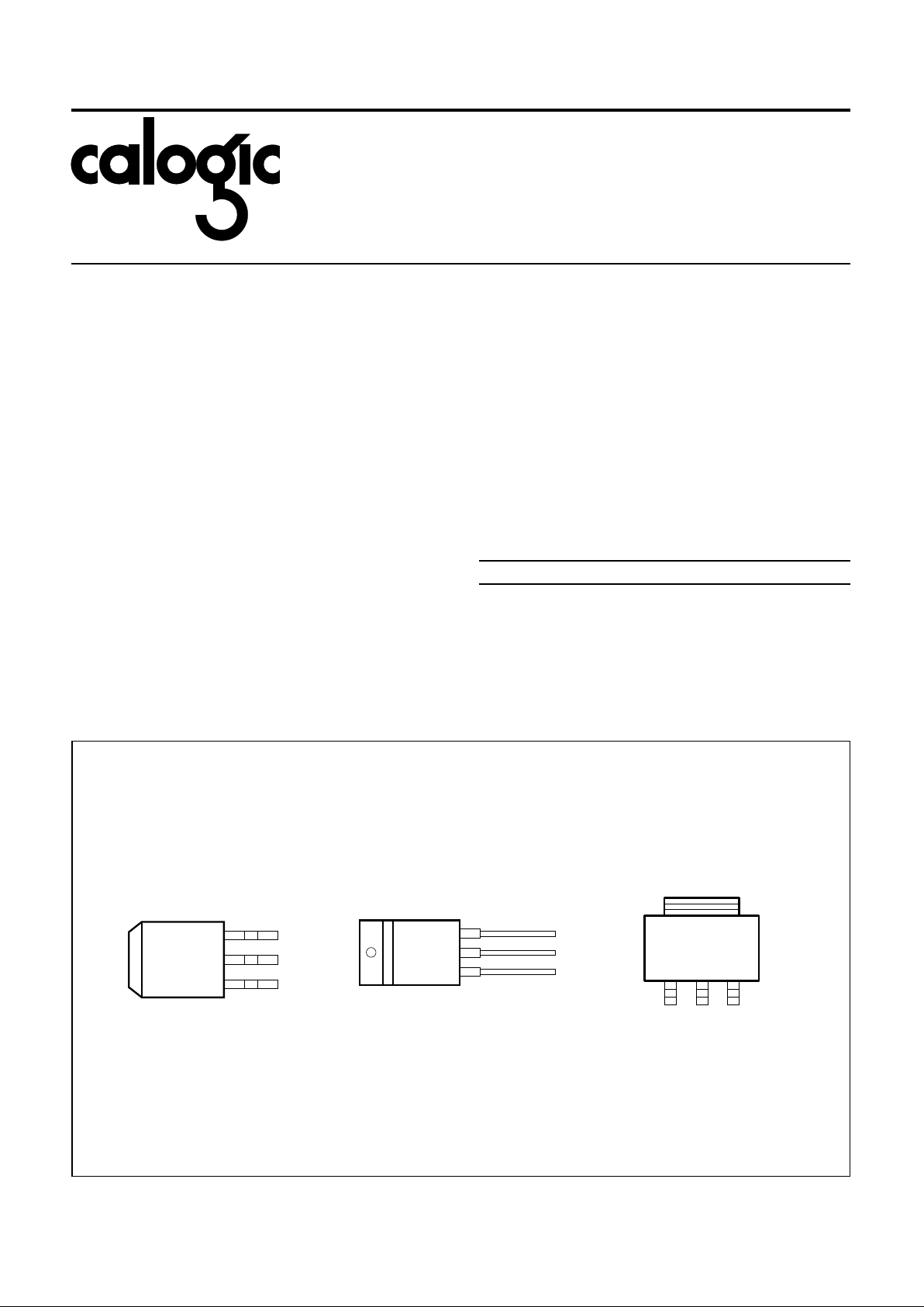
•• Surface Mou nt Packag e SO T-223, DD PAK a n d TO-22 0
APPLICATIONS
•• SCSI-II Active Terminator
•• Portable/Palm Top/Notebook Computers
•• Battery Charger s
•• Disk Driv es
•• Portable Consumer Equipment
•• Portable I nst ru me nt atio n
•• SMPS Post-Regula tor
DESCRIPTION
The CLM2810 is a low power, positive voltage regulator. The
device has been designed to provide an output current of 1A
while complying with SCSI-II specifications with a fixed output
voltage of 2.85V. Applications include battery-powered and
portable computers. The device has a low quiescent current
while providing 1.2V drop-out voltage at a full load. Pr oduct is
available as an adjustable LDO or fixed 2.85V , 3.0V, 3.3V and
5.0V output voltages.
ORDERING INFORMATION
Part Package Description Temperature
CLM2810U TO-220 Adjustable -40
o
C to +85oC
CLM2810M SOT-223 Adjustable -40
o
C to +85oC
CLM2810U-X TO-220 X = output voltage -40
o
C to +85oC
CLM2810M-X SOT-223 M = output voltage -40
o
C to +85oC
CLM2810AT DD Adjustable -40
o
C to +85oC
CLM 2 810AT-X DD X = output voltage -40
o
C to +85oC
CORPORATION
PIN CONNECTIONS
1T-29
FRONT VIEW
V
IN
V
OUT
CLM2810-3.3
PLASTIC PACKAGE TO-220
GND
1T-28
PLASTIC DD PACKAGE
FRONT VIEW
CLM2810
3
2
1V
ADJ
V
OUT
V
IN
SOT-223
TAB IS
GND
CLM2810
GND
123
1T-30
FRONT VIEW
V
OUTVIN
CALOGIC CORPORATION, 237 Whitne y Pl a ce , Fr emo n t , Califo rn i a 94 5 39 , Telephone: 510-65 6-2 900, FAX: 510-651-3025
ABSOLUTE MAXIMUM RATINGS
Power Dissipation . . . . . . . . . . . . . . . . . . . . . Internally Limited
Lead Temp. (Soldering, 5 Sec onds) . . . . . . . . . . . . . . . 26 0 °C
Storage Temper atur e Range . . . . . . . . . . . . . . -65° to +15 0°C
Operating Junct ion Tem per atur e Ran ge. . . . -4 0 C° to +125° C
Input V olt age . . . . . . . . . . . . . . . . . . . . . . . . . . . . . . 2.5V to 6V
Input Supply Vo ltag e . . . . . . . . . . . . . . . . . . . . . -20V to +20V
ESD Rating . . . . . . . . . . . . . . . . . . . . . . . . . . . . . . . . 2KV M in
CLM2810
CORPORATION
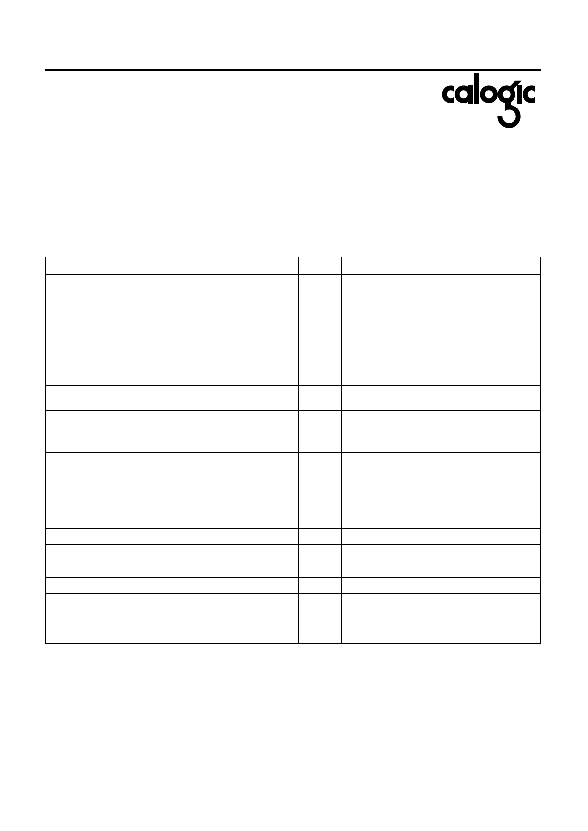
ELECTRICAL CHARACTERISTICS: VIN = V
OUT
+1, TA = 25oC, CL = 3.3µf, unless otherwise noted. Boldface apply over full
operating temperature range.
PARAMETER TYP MIN MAX UNITS CONDITIONS
Output Voltage
2.85
2.85
2.85
3.0
3.0
3.30
3.30
5.0
5.0
2.82
2.79
2.79
2.97
2.94
3.27
3.24
4.95
4.90
2.88
2.91
2.91
3.03
3.06
3.33
3.36
5.05
5.10
V
I
OUT
= 10mA, VIN = 4.85V
0 ≤ I
OUT
≤ 1A, 4.25 ≤ VIN ≤ 10V
0 ≤ I
OUT
≤ 500mA, VIN = 4.05V
I
OUT
= 10mA, VIN = 5.00V
0 ≤ I
OUT
≤ 1A, 4.50 ≤ VIN ≤ 10V
I
OUT
= 10mA, VIN = 5.30V
0 ≤ I
OUT
≤ 1A, 4.80 ≤ VIN ≤ 10V
I
OUT
= 10mA, VIN = 7.00V
0 ≤ I
OUT
≤ 1A, 6.50 ≤ VIN ≤ 12V
Output Voltage
T emperature Stability
0.05 % (Note 1)
Line Regulation
1.00
1.00
1.00
1.00
6.00
7.00
7.00
10.00
mV
4.25V ≤ V
IN
≤ 10V, V
OUT
= 2.85, I
OUT
= 0
4.50V ≤ V
IN
≤ 12V, V
OUT
= 3.00, I
OUT
= 0
4.80V ≤ V
IN
≤ 12V, V
OUT
= 3.30, I
OUT
= 0
6.50V ≤ V
IN
≤ 15V, V
OUT
= 5.00, I
OUT
= 0
Load Regulation
1.00
1.00
1.00
1.00
10.00
12.00
12.00
15.00
mV
0 ≤ I
OUT
≤ 1A, VIN = 4.25V, V
OUT
= 2.85
0 ≤ I
OUT
≤ 1A, VIN = 4.50V, V
OUT
= 3.00
0 ≤ I
OUT
≤ 1A, VIN = 4.80V, V
OUT
= 3.30
0 ≤ I
OUT
≤ 1A, VIN = 6.50V, V
OUT
= 5.00
Dropout Voltage
(Note 2)
1.00
1.05
1.10
1.10
1.15
1.20
V
I
L
= 100m A
I
L
= 500m A
I
L
= 1A
Quiescent Current 5.00 10.00 mA 4.25V ≤ V
IN
≤ 6.5V
Current Limit 800 950 1200 mA (V
IN
- V
OUT
) = 5V
Thermal Regulation 0.01 0.1 %/W 25
o
C, 30ms Pulse
Ripple Rejection 60 75 dB f
RIPPLE
= 12 0H z, (VIN - V
OUT
) = 3V, V
RIPPLE
= 1V
p-p
Long Term Stability 0.03 % 125oC, 1000Hrs
RMS Output Noise 0.003 % % of V
OUT
, 10Hz ≤ f ≤ 10kHz
Thermal Resistance 15
o
C/WoJunction to case, at tab
Note 1: Output temperature coeffic ien t is define d as the worst case volta ge change divid ed by the total tempe rature range .
Note 2: Dropout voltage is defined as the input to output differential at which the output voltage drops 100mV below its nominal value measured
at 1V differential at very low values of programmed output voltage, the minimum input supply voltage of 2V (2.3V over temperature) must be
taken input account.
Note 3: Thermal regulation is defined as the change in output voltage at a time T after a change in power dissipation is applied,
excluding load or line regulation effect.
CALOGIC CORPORATION, 237 Whitne y Pl a ce , Fr emo n t , Califo rn i a 94 5 39 , Telephone: 510-65 6-2 900, FAX: 510-651-3025
 Loading...