

Burr Brown Corporation DDC101U Datasheet
20-BIT ANALOG-TO-DIGITAL CONVERTER
DDC101
DESCRIPTION
The DDC101 is a precision, wide dynamic range, charge
digitizing A/D converter with 20-bit resolution. Low
level current output devices, such as photosensors, can be
directly connected to its input. The most stringent accuracy requirements of many unipolar output sensor applications occur at low signal levels. To meet this requirement, Burr-Brown developed the adaptive delta modulation architecture of the DDC101 to provide linearly
improving noise and linearity errors as the input signal
level decreases. The DDC101 combines the functions of
current-to-voltage conversion, integration, input programmable gain amplification, A/D conversion, and digital
filtering to produce precision, wide dynamic range results. The input signal can be a low level current connected directly into the unit or a voltage connected
through a user selected resistor. Although the DDC101 is
optimized for unipolar signals, it can also accurately
digitize bipolar input signals. The patented delta modula-
tion topology combines charge integration and digitization functions. Oversampling and digital filtering reduce
system noise dramatically. Correlated Double Sampling
(CDS) captures and eliminates steady state and conversion cycle dependent offset and switching errors that are
not eliminated with conventional analog circuits.
The DDC101 block diagram is shown below. During
conversion, the input signal is collected on the internal
integration capacitance for a user determined integration
period. A high precision, autozeroed comparator samples
the analog input node. Tracking logic updates the internal
high resolution D/A converter at a 2MHz rate to maintain
the analog input at virtual ground. A user programmable
digital filter oversamples the tracking logic’s output. The
digital filter passes a low noise, high resolution digital
output to the serial I/O register. The serial outputs of
multiple DDC101 units can be easily connected together
in series or parallel if desired to minimize interconnections.
● MONOLITHIC CHARGE INPUT ADC
● DIGITAL FILTER NOISE REDUCTION:
0.9ppm, rms
● DIGITAL ERROR CORRECTION: CDS
● CONVERSION RATE: Up to 15kHz
● USER FRIENDLY EVALUATION FIXTURE
APPLICATIONS
FEATURES
● DIRECT PHOTOSENSOR DIGITIZATION
● PRECISION INSTRUMENTATION
● INFRARED PYROMETRY
● PRECISION PROCESS CONTROL
● CT SCANNER DAS
● CHEMICAL ANALYZERS
C
INT
Digital Integration,
Tracking and
Control Logic
Digital Filter and
Error Correction
Serial I/O
Register
Serial In
Serial Out
Reset
DAC
CDAC
DDC101 Integrated Circuit
Comparator
V
REF
Analog
Input
Ground
Setup
Oversampled
Digital Out
18 Bits
20 Bits
Test In
+V
S
Test Current
©
1993 Burr-Brown Corporation PDS-1211E Printed in U.S.A. March, 1998
®
International Airport Industrial Park • Mailing Address: PO Box 11400, Tucson, AZ 85734 • Street Address: 6730 S. Tucson Blvd., Tucson, AZ 85706 • Tel: (520) 746-1111 • Twx: 910-952-1111
Internet: http://www.burr-brown.com/ • FAXLine: (800) 548-6133 (US/Canada Only) • Cable: BBRCORP • Telex: 066-6491 • FAX: (520) 889-1510 • Immediate Product Info: (800) 548-6132
DDC101
®
DDC101
2
TABLE OF CONTENTS
Section 1 ............. Basic Theory of Operation
2 ............. Specifications
3 ............. Pin Descriptions
4 ............. Timing Diagrams
5 ............. Discussion of Specifications
6 ............. Detailed Theory of Operation
7 ............. Applications Information
8 ............. Mechanical
The second block diagram, Figure 2, shows the DDC101
circuit architecture which implements these functions
monolithically. During each conversion, the input signal
current is collected on the internal integration capacitance,
C
INT
, as charge for a user determined integration period, T
INT
.
As the integration capacitor collects input charge, the tracking logic updates the internal high resolution D/A converter
at a 2MHz rate to maintain the analog input node at virtual
ground.
The digital filter oversamples the tracking logic’s output at
the beginning and end of each integration period to produce
two oversampled data points. The DDC101 measures the
charge accumulated in the integration and performs correlated double sampling (CDS) by subtracting these two data
points. CDS eliminates integration cycle dependent errors
such as charge injection, offset voltage, and reset noise since
these errors are measured with the signal at each of the two
data points. The number of oversamples, and thus the frequency response of the digital filter, is user programmable.
The digital filter passes a low noise, high resolution digital
output to the serial I/O register. Since the timing control of
the serial I/O register is independent of the DDC101 conversion process, the outputs of multiple DDC101 units can be
connected together in series or parallel to minimize interconnections.
SECTION 1
BASIC THEORY OF OPERA TION
The basic function of the DDC101 is illustrated in the
Simplified Equivalent Circuit shown in Figure 1. The operation is equivalent to the functions performed by a very high
quality, low bias current switched integrator followed by a
precision floating point programmable gain amplifier and
ending with a high resolution A/D converter.
FIGURE 1. Simplified Equivalent Circuit of DDC101 to Illustrate Function.
FIGURE 2. DDC101 Block Diagram.
C
INT
Digital Integration,
Tracking and
Control Logic
Digital Filter and
Error Correction
Serial I/O
Register
Serial In
Serial Out
Reset
DAC
CDAC
DDC101 Integrated Circuit
Comparator
V
REF
Analog
Input
Ground
Setup
Oversampled
Digital Out
18 Bits
20 Bits
Test In
+V
S
Test Current
C
INT
Data Out
Reset
Switched Integrator
Programmable Gain
Amplifier
A/D Converter
and Control Logic
Sensor
i Signal
3
DDC101
®
The information provided herein is believed to be reliable; however, BURR-BROWN assumes no responsibility for inaccuracies or omissions. BURR-BROWN
assumes no responsibility for the use of this information, and all use of such information shall be entirely at the user’s own risk. Prices and specifications are subject
to change without notice. No patent rights or licenses to any of the circuits described herein are implied or granted to any third party. BURR-BROWN does not
authorize or warrant any BURR-BROWN product for use in life support devices and/or systems.
An internal test current source is provided for basic functionality testing and diagnostics. This approximately 100nA
current source is pin activated and sums with the external
input current.
Figure 3 shows a more detailed circuit configuration of the
DDC101. The single integration capacitor, C
INT
, and the
D/A converter have been replaced with a high resolution
Capacitor Digital-to-Analog Converter (CDAC). By switching between ground and V
REF
the binary weighted capacitor
array of the CDAC accumulates the input signal’s charge to
keep the comparator input at virtual ground.
FIGURE 3. DDC101 Detailed Circuit Diagram.
Reset
Comparator
Sensor
Serial I/O
Register
DATA
INPUT
DATA
OUTPUT
High
Resolution
Digital Out
3rd Order Digital
Integration,
Tracking and
Control Logic
Digital
Filter
Oversampled
Digital Out
C
INT
Buffer
V
REF
SYSTEM
CLOCK
System Control DATA
CLOCK
DATA
TRANSMIT
CDAC
DDC101
+V
S
Test Current
TEST
In
ANALOG
In
ANALOG
COMMON
18 Bits
20 Bits
®
DDC101
4
SECTION 2
SPECIFICATIONS
ELECTRICAL
All specifications with unipolar current input range, T
INT
= 1ms, correlated double sampling enabled, System Clock = 2MHz, V
REF
= –2.5V, TA = +25°C and VS = ±5VDC,
unless otherwise noted.
DDC101
PARAMETER CONDITIONS MIN TYP MAX UNITS
INPUTS
Charge Input
(6)
Unipolar Input Range BTC Output Code –1.95 500 pC/Integration
Bipolar Input Range BTC Output Code –251.95 250 pC/Integration
Input Current Unipolar or Bipolar Range 7.8 µA
Current Input Range Examples
(10)
Unipolar Input Range T
INT
= 100µs –0.0195 5 µA
Unipolar Input Range T
INT
= 1ms –1.95 500 nA
Bipolar Input Range T
INT
= 100µs –2.5195 2.5 µA
Bipolar Input Range T
INT
= 1ms –251.95 250 nA
Voltage Input Examples
(10)
Unipolar Input Range
(2)
RIN = 10MΩ, T
INT
= 1ms –0.0195 5 V
Bipolar Input Range
(2)
RIN = 10MΩ, T
INT
= 1ms –2.5195 2.5 V
DYNAMIC CHARACTERISTICS
Conversion Time 64 256 x 10
6
µs
Integration Time 64 10
6
µs
System Clock Input 0.5 2 MHz
ACCURACY
Unipolar Mode Noise
Noise, Low Level Current Input
(1)
C
SENSOR
= 0pF, L = 8 0.9 ppm of FSR, rms
(3)
Noise, Low Level Current Input
(1)
C
SENSOR
= 0pF, L = 1 1.6 ppm of FSR, rms
Noise, Low Level Current Input
(1)
C
SENSOR
= 100pF, L = 1 2.1 3 ppm of FSR, rms
Noise, Low Level Current Input
(1)
C
SENSOR
= 500pF, L = 1 4.2 ppm of FSR, rms
Noise, Voltage Input
(1, 2)
RIN ≥ 20MΩ 1.9 ppm of FSR, rms
Differential Linearity Error
Unipolar Input Range Entire Range ±0.005% Reading ±0.5ppm FSR, max
0.1% FSR Input ±0.00006 % of FSR
1% FSR Input ±0.00010 % of FSR
10% FSR Input ±0.00055 % of FSR
Unipolar or Bipolar Input Range ±0.0015 % of FSR
Integral Linearity Error
Unipolar Input Range
(11)
0 to 500 pc/Integration ±0.0244% Reading ±2.5ppm FSR, max
–1.95 to 0 pc/Integration ±0.0244% Reading ±3.0ppm FSR, max
0.1% FSR Input ±0.00028 % of FSR
1% FSR Input ±0.00050 % of FSR
10% FSR Input ±0.0027 % of FSR
Unipolar or Bipolar Input Range
(11)
±0.003 % of FSR
No Missing Codes
Unipolar Input Range 18 Bits
Bipolar Input Range 16 Bits
Input Bias Current T
A
= +25°C310pA
DC Gain Error ±0.5 ±2 % of FSR
Output Offset Error
(8)
±0.5 ppm of FSR
Input Offset Voltage
(8)
±0.5 ±2mV
External Voltage Reference, V
REF
–2.5 VDC
Internal Test Signal 100 nA
Internal Test Signal Accuracy ±20 nA
Gain Sensitivity to V
REF
V
REF
= 2.5V ±0.1V 1:1
PSRR 80 90 dB
PERFORMANCE OVER TEMPERATURE
Output Offset Drift
(8)
not including bias current drift 0 µV/°C
Input Offset Voltage Drift
(8)
1 µV/°C
Input Bias Current Drift +25°C to +45°C 0.1 0.5 pA/°C
Input Bias Current T
A
= +85°C840pA
Gain Drift
(4)
±15 ppm/°C
DIGITAL INPUT/OUTPUT
Logic Family TTL Compatible CMOS
Logic Level: V
IH
IIH = +5µA +2.0 +V
CC
V
V
IL
IIL = +5µA –0.3 +0.8 V
V
OH
IOH = 2 TTL Loads +2.4 +V
CC
V
V
OL
IOL = 2 TTL Loads 0.0 0.4 V
Data Clock
Data I/O 8 MHz
SETUP Code I/O
(9)
4 MHz
Data Format
Straight Binary Unipolar or Bipolar Range 20 Bits
Two’s Complement Unipolar or Bipolar Range 21 Bits
5
DDC101
®
SPECIFICATIONS (CONT)
ELECTRICAL
All specifications with unipolar current input range, T
INT
= 1ms, correlated double sampling enabled, System Clock = 2MHz, V
REF
= –2.5V, TA = +25°C and VS = ±5VDC,
unless otherwise noted.
DDC101
PARAMETER CONDITIONS MIN TYP MAX UNITS
POWER SUPPLY REQUIREMENTS
Operation
(5)
±4.75 ±5 ±5.25 VDC
Quiescent Current, Positive Supply V
S
+ = +5VDC, VDD+ = +5VDC 15.6 19.5 mA
Analog, V
S
+ 8.9 mA
Digital, V
DD
+ 6.7 mA
Quiescent Current, Negative Supply V
S
– = –5VDC 18.0 22.5 mA
Operating Power 170 mW
TEMPERATURE RANGE
Operating –40 +85 °C
Storage –60 +100 °C
NOTES: (1) Input = low level (less than 1% of Full Scale); Full Scale I
IN
= 500nA; T
INT
= 1ms; Unipolar Input Range; Acquisition Time = 16 clock cycles, Oversampling = 128. (2) Voltage input is converted through user
provided input resistor, R
IN
. (3) FSR is Full Scale Range. (4) Gain Drift does not include the drift of the external reference. (5) V
DD
+ must be less than or equal to VS+. See Section 7 for recommended connections. (6)
Straight Binary output code has slightly different Charge Range. See Section 6. (8) Input offset voltage is nulled by autozero circuitry and causes no output error. See Section 6 (Internal Error Correction). (9) This is
the maximum clock frequency at which SETUP codes can be written to and read from the DDC101. (10) For other input current and voltage configurations, see Discussion of Specifications and Detailed Theory of Operation
sections. (11) A best-fit straight line method is used to determine linearity. Two different best-fit straight lines are used for the two unipolar integral linearity specifications. Acquisition Time = 16 clock cycles, Oversampling
= 128.
Analog Inputs
Input Current ............................................................ 100mA, momentary
Input Current .............................................................. 10mA, continuous
Input Voltage ................................................... V
S
+ +0.5V to VS– –0.5V
Power Supply
V
S
+ .................................................................................................. + 7V
V
S
– ....................................................................................................–7V
V
DD
+ ................................................................................. must be ≤ VS+
Maximum Junction Temperature ................................................... +165°C
ABSOLUTE MAXIMUM RATINGS
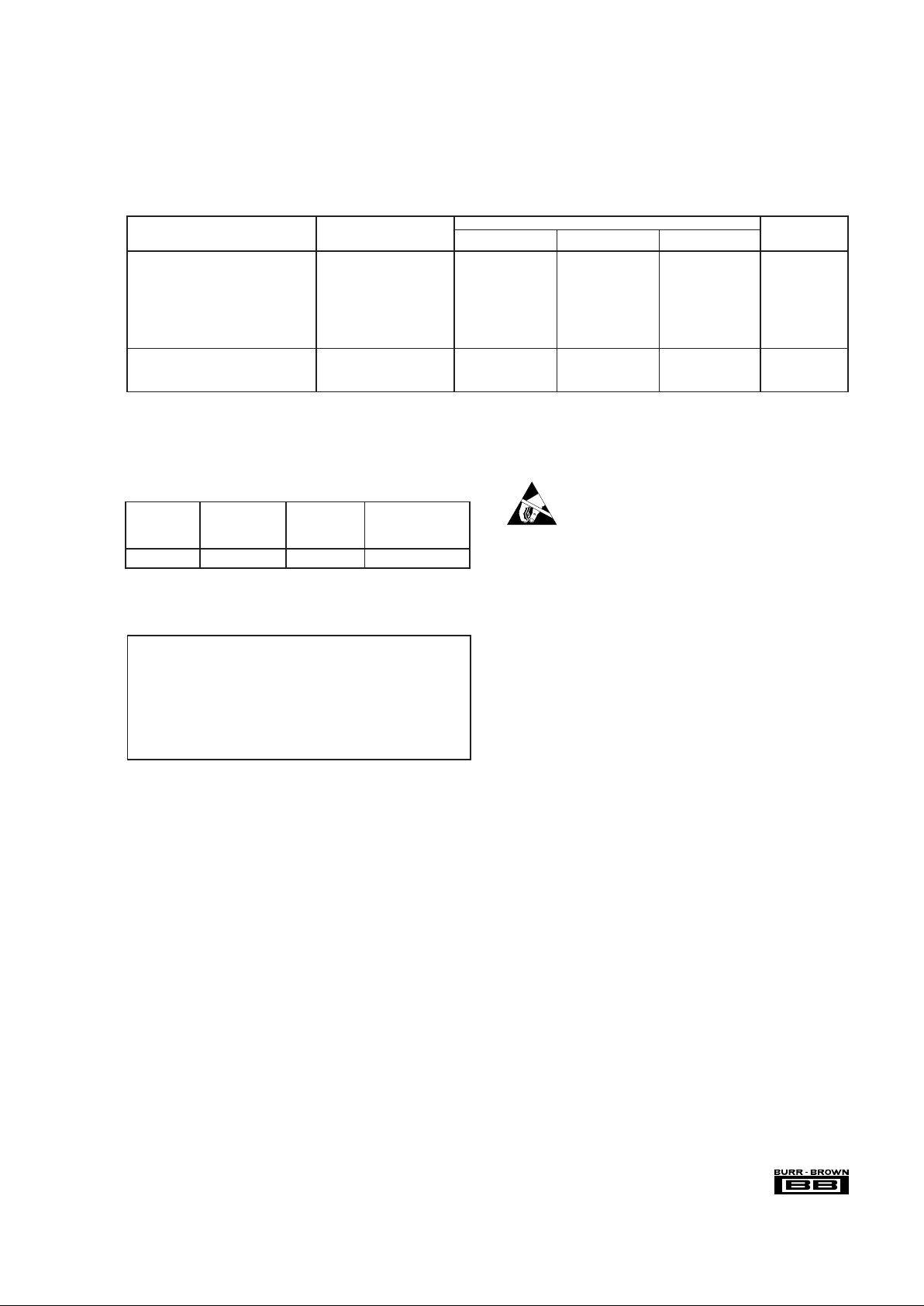
PACKAGE/ORDERING INFORMATION
PACKAGE THERMAL
DRAWING RESISTANCE (
θ
JA
)
PRODUCT PACKAGE NUMBER
(1) (°C/W)
DDC101U 24-Lead SOIC 239 100
NOTE: (1) For detailed drawing and dimension table, please see end of data
sheet, or Appendix C of Burr-Brown IC Data Book.
The information provided herein is believed to be reliable; however, BURR-BROWN assumes no responsibility for inaccuracies or omissions. BURR-BROWN assumes
no responsibility for the use of this information, and all use of such information shall be entirely at the user’s own risk. Prices and specifications are subject to change
without notice. No patent rights or licenses to any of the circuits described herein are implied or granted to any third party. BURR-BROWN does not authorize or warrant
any BURR-BROWN product for use in life support devices and/or systems.
ELECTROSTATIC
DISCHARGE SENSITIVITY
This integrated circuit can be damaged by ESD. Burr-Brown
recommends that all integrated circuits be handled with appropriate precautions. Failure to observe proper handling and
installation procedures can cause damage.
ESD damage can range from subtle performance degradation
to complete device failure. Precision integrated circuits may
be more susceptible to damage because very small parametric
changes could cause the device not to meet published
specifications.
®
DDC101
6
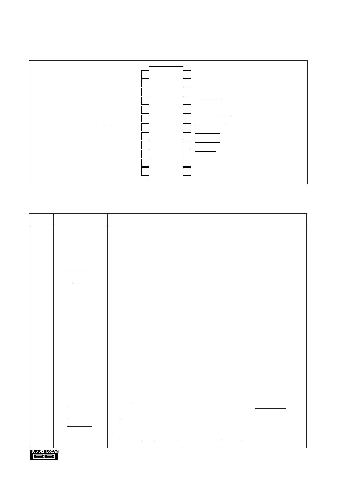
PIN CONFIGURATION
Top View 24-Lead SOIC
SECTION 3
PIN DESCRIPTIONS
1
2
3
4
5
6
7
8
9
10
11
12
24
23
22
21
20
19
18
17
16
15
14
13
REFERENCE BUFFER BYPASS
V
REF
TEST In
RESET SETUP In
SETUP
READ DATA/SETUP
DATA TRANSMIT In
OVERFLOW + Out
OVERFLOW – Out
DATA VALID Out
DATA OUTPUT
DIGITAL GROUND
V
S
–, ANALOG
ANALOG COMMON
ANALOG In
ANALOG COMMON
V
S
+, ANALOG
V
S
+, ANALOG
RESET SYSTEM In
FDS (Final Data Point Start) In
SYSTEM CLOCK
DATA CLOCK
DATA INPUT
V
DD
+, DIGITAL
PIN
NUMBER NAME DESCRIPTION
1V
S
–, ANALOG Negative analog power supply voltage, –5VDC.
2 ANALOG COMMON Analog ground point.
3 ANALOG INPUT Input for low level current signal. Photosensor can be directly connected to this input. With a resistor in series,
DDC101 will convert a voltage input.
4 ANALOG COMMON Analog ground point.
5V
S
+, ANALOG Positive analog power supply voltage, +5VDC. Hardwire to pin 6.
6V
S
+, ANALOG Positive analog power supply voltage, +5VDC. Hardwire to pin 5.
7 RESET SYSTEM In This input resets DDC101, but does not reset the SETUP register. The DDC101 system is reset when this pin
is active; reset action is removed when the pin is inactive.
8 FDS In This is Final Data point Start input. This input is the basic user control of the integration and conversion timing.
When it becomes active, the DDC101 starts collection of the M, final data point samples. The beginning of the
next integration time is exactly M system clock periods after the Final Data point Start command when operating
in the continuous mode.
9 SYSTEM CLOCK This clock input sets the basic sampling rate of the DDC101. The DDC101 is specified with a clock speed of
2MHz. The clock speed can be 0.5MHz to 2.0MHz.
10 DATA CLOCK This clock input controls the data transfer rate for the serial DATA INPUT and DATA OUTPUT ports. The DATA
CLOCK is independent of the SYSTEM CLOCK. This allows the DATA CLOCK to be operated at higher or lower
speeds than the SYSTEM CLOCK. For best noise performance, data should not be transmitted and the DATA
CLOCK should not be active during the initial and final data point collection. If data is being transmitted during
the initial and final data point collection periods, the DATA CLOCK should be synchronized to the SYSTEM
CLOCK, to minimize added noise. DATA CLOCK can be connected to SYSTEM CLOCK, so that the same clock
is used for both; however, for best noise performance, the DATA CLOCK input should be active only when data
is transmitted.
11 DATA INPUT This input can be used to “daisy chain” the output of several DDC101s together to minimize wiring. The output
register of the DDC101 acts as a shift register to pass through the output of previously connected DDC101 units.
In this way, multiple DDC101 units can convert simultaneously then sequence the data out serially on the same
data line with one common control line and one common data line for all DDC101 units.
12 V
DD
+, DIGITAL Digital power supply, +5VDC. VDD+ must be less than or equal to VS+.
13 DIGITAL GROUND Digital ground point.
14 DATA OUTPUT This output provides serial digital data clocked out at user controlled DATA CLOCK rate. Output data format
is a 21-bit Binary Two's Complement word or a 20-bit Straight Binary word. The data word is transmitted MSB
first. When DATA TRANSMIT is not active DATA OUTPUT tri-states.
15 DATA VALID This output is activated when conversion is complete and remains active until the DATA TRANSMIT input is
activated.
16 OVERFLOW– The OVERFLOW output signals each provide an open collector output so that the overflow outputs from several
17 OVERFLOW+ DDC101s can easily be connected (wire ORed) together to a common pull-up resistor. They are activated when
the input is beyond the acceptable range during conversion. Specifically, they are activated when the internal
D/A converter input or digital filter exceeds full scale. They are Cleared at the end of conversion 1/2 clock cycle
after DATA VALID high. DATA VALID can be used to capture OVERFLOW data into an external register.
7
DDC101
®
PIN DESCRIPTIONS (CONT)
PIN
NUMBER NAME DESCRIPTION
18 DATA TRANSMIT In This input controls the transmission of data from the serial I/O register of the DDC101. It can be activated
anytime after DATA VALID out becomes active. It must remain active until all data has been collected from the
serial I/O register(s) of all DDC101s in the data path.
19 READ DATA/ This input can be used to read back the current SETUP data. When this input is held high, the output from DATA
SETUP In OUTPUT is the data collected by the DDC101. When this input is pulled low, an internal shift register is loaded
with the current SETUP data on the rising edge of DATA CLOCK. This SETUP data shift register is logically
connected between DATA INPUT and DATA OUTPUT pins and can be read in the same way that the data
output is read. SETUP data read back does not invalidate data already stored in the DDC101's serial I/O register
or data being collected by the DDC101, although digital noise concerns should be considered as
discussed in DATA CLOCK.
20 SETUP In This input pin controls the DDC101 SETUP. A 12-bit digital word transmitted into this pin controls Acquisition
Time, K, Oversampling, M, Multiple Integrations, L, Input Range and Output Data Format. The DDC101 reads
the SETUP code at this pin after the RESET SETUP input transitions from active to inactive. The SETUP code
is read into the SETUP register on the 12 positive data clock transitions following that transition.
21 RESET SETUP Resets SETUP register only, does not reset balance of DDC101. The DDC101 reads SETUP input data after
this input transitions from active (reset) to inactive.
22 TEST In This is a digital input that controls the connection of an internal DC current source to the DDC101's input. TEST
In exercises the DDC101 and is intended to test for functionality only. The typical test input current is 100nA
±20nA. The quiescent current of the DDC101 increases by approximately 1mA when TEST In is active. When
TEST is HIGH, the internal current source is ON and current is flowing into the DDC101 input. When TEST is
LOW, the current source is disconnected from the input.
23 V
REF
An external –2.5V reference must be connected to the REFERENCE In pin. Use of an external reference allows
multiple DDC101s to use the same system reference for optimum channel matching. The external reference
should be filtered to minimize noise contribution (see Figure 24).
24 REFERENCE An external capacitor of 10µF should be connected to this node to provide proper operation of the internal
BUFFER BYPASS D/A converter. The REFERENCE In pin is connected to an internal reference buffer
amplifier. The internal reference buffer drives the internal CDAC. This buffer output is not intended for external
use.
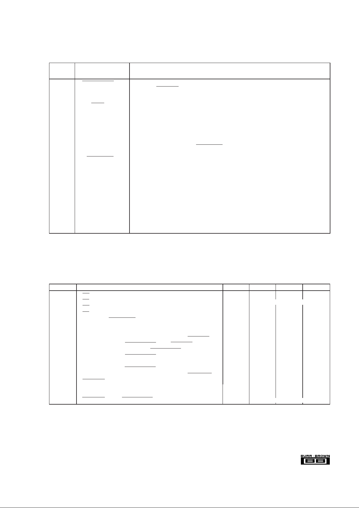
SECTION 4
TIMING CHARACTERISTICS
All specifications with Unipolar input range, T
INT
= 1ms, Current Input, Correlated Double Sampling enabled, Sys Clock = 2MHz, V
REF
= –2.5V, TA = +25°C and
V
S
= ±5VDC, unless otherwise noted.
SYMBOL DESCRIPTION MIN TYP MAX UNITS
t
1
FDS Setup 30 ns
t
2
FDS width, Continuous Conversion 50 (M–1) Clocks+t1+100ns ns
t
3
FDS width, Asynchronous Conversion M Clocks+t
1
ns
t
4
FDS HIGH to start of next integration, Asynchronous Conversion 50 ns
t
5
Setup time for RESET SETUP HIGH to DATA CLOCK HIGH 60 ns
t
6
Setup time for Setup Codes data valid before rising edge of DATA Clock 30 ns
t
7
Hold time for Setup Codes data valid after rising edge of DATA Clock 30 ns
t
8
Propagation delay from rising edge of SYSTEM CLOCK to DATA VALID LOW 50 ns
t
9
Propagation delay from DATA TRANSMIT LOW to DATA VALID HIGH 35 ns
t
10
Setup time for DATA CLOCK LOW to DATA TRANSMIT LOW 30 ns
t
11
Propagation delay from DATA TRANSMIT LOW to valid data out 30 ns
t
12
Hold time that Data output is valid after falling edge of DATA CLOCK 10 ns
t
13
Propagation delay from DATA TRANSMIT HIGH to Data Output tri-stated 40 ns
t
14
Propagation delay from falling edge of SYSTEM CLOCK to OVERFLOW+ and 25 ns
OVERFLOW–cleared
t
15
SYSTEM CLOCK pulse width HIGH 240 ns
t
16
SYSTEM CLOCK pulse width LOW 240 ns
t
17
DATA VALID LOW to DATA TRANSMIT LOW, Single DDC101 30 (LxN–21) Clocks ns
®
DDC101
8
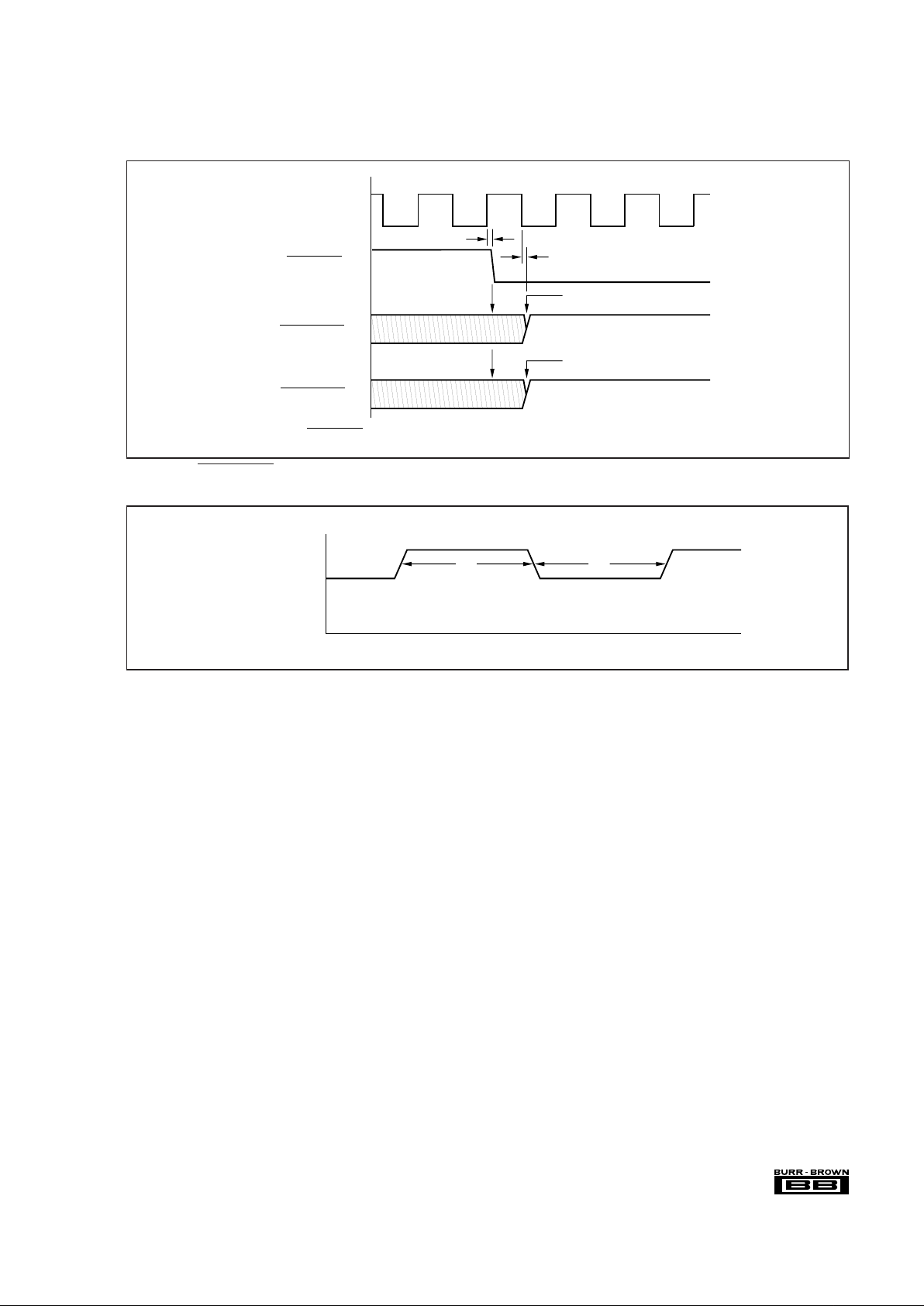
FIGURE 6. DATA TRANSMIT Timing Diagram.
FIGURE 4. Conversion Timing Diagrams.
Input
Range
Output
Format
SETUP In
DATA CLOCK
(4MHz, max for setup)
ACQ
LSB
t
5
RESET SETUP In
ACQ
MSB
Read Read Read Read
t
6
t
7
FIGURE 5. Input/Output Timing Diagram—SETUP Timing Diagram.
SYSTEM
CLOCK
DATA VALID
Out
DATA TRANSMIT
In
DATA OUTPUT
DATA CLOCK
(8MHz, max for data)
t
10
DDC(1)
Bit 1, MSB
DDC(n)
Bit 21, LSB
DDC
(n+1)
Bit 1
Output Disabled
Last DDC
Bit 21
Output Enabled
Output Disabled
t
12
Data can be read on rising or falling edge of Data Clock
DATA TRANSMIT In resets DATA VALID Out.
t
9
t
11
t
13
t
17
t
8
Continuous Integration Timing
Non-Continuous Integration Timing
SYSTEM
CLOCK
FDS In
Internal
Oversampling
Interval
Internal
Reset
SYSTEM
CLOCK
FDS In
Internal
Oversampling
Interval
Internal
Reset
FDS In should be coincident with negative clock.
FDS initiates oversampling period.
M Clock Periods
End of oversample period
initiates reset for next integration.
FDS In should be coincident with negative clock.
FDS initiates oversampling period.
End of FDS In
initiates end of Internal Reset.
End of oversample
period initiates
reset.
When Internal Reset period ends,
next integration begins.
DATA VALID
Out
t
2
t
1
t
3
DATA VALID Out
Next integration begins when 1 clock
period wide Internal Reset ends.
M Clock Periods
t
4
T
INT
'
T
INT
9
DDC101
®
TIMING DIAGRAMS (CONT)
FIGURE 7. OVERFLOW Out Monitoring Timing Diagram.
OVERFLOW – Out
OVERFLOW + Out
t
8
DATA VALID Out
Read
Read
Clear
SYSTEM CLOCK In
t
14
DATA VALID Out can be used to latch data from the overflow status outputs.
Clear
FIGURE 8. System Clock Timing.
t
15
SYSTEM CLOCK In
SYSTEM CLOCK
t
16
 Loading...