

Burr Brown Corporation DAC904E-2K5, DAC904E, DAC904U-1K, DAC904U Datasheet
®
For most current data sheet and other product
information, visit www.burr-brown.com
DAC904
DAC904
DAC904
14-Bit, 165MSPS
DIGITAL-TO-ANALOG CONVERTER
FEATURES
● SINGLE +5V OR +3V OPERATION
●
HIGH SFDR: 20MHz Output at 100MSPS: 64dBc
● LOW GLITCH: 3pV-s
● LOW POWER: 170mW at +5V
● INTERNAL REFERENCE:
Optional Ext. Reference
Adjustable Full-Scale Range
Multiplying Option
DESCRIPTION
The DAC904 is a high-speed, digital-to-analog converter (DAC)
offering a 14-bit resolution option within the SpeedPlus family
of high-performance converters. Featuring pin compatibility
among family members, the DAC908, DAC900, and DAC902
provide a component selection option to an 8-, 10-, and 12-bit
resolution, respectively. All models within this family of D/A
converters support update rates in excess of 165MSPS with
excellent dynamic performance, and are especially suited to
fulfill the demands of a variety of applications.
The advanced segmentation architecture of the DAC904 is
optimized to provide a high Spurious-Free Dynamic Range
(SFDR) for single-tone, as well as for multi-tone signals—
essential when used for the transmit signal path of communication systems.
The DAC904 has a high impedance (200kΩ) current output with
a nominal range of 20mA and an output compliance of up to
1.25V. The differential outputs allow for both a differential, or
single-ended analog signal interface. The close matching of the
current outputs ensures superior dynamic performance in the
differential configuration, which can be implemented with a
transformer.
Utilizing a small geometry CMOS process, the monolithic
DAC904 can be operated on a wide, single-supply range of
+2.7V to +5.5V. Its low power consumption allows for use in
portable and battery operated systems. Further optimization can
be realized by lowering the output current with the adjustable
full-scale option.
TM
APPLICATIONS
● COMMUNICATION TRANSMIT CHANNELS
WLL, Cellular Base Station
Digital Microwave Links
Cable Modems
● WAVEFORM GENERATION
Direct Digital Synthesis (DDS)
Arbitrary Waveform Generation (ARB)
● MEDICAL/ULTRASOUND
● HIGH-SPEED INSTRUMENTATION AND
CONTROL
● VIDEO, DIGITAL TV
For noncontinuous operation of the DAC904, a power-down
mode results in only 45mW of standby power.
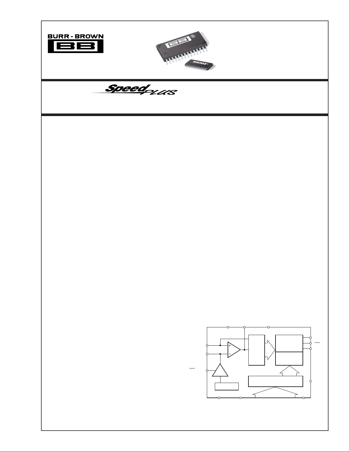
The DAC904 comes with an integrated 1.24V bandgap reference and edge-triggered input latches, offering a complete
converter solution. Both +3V and +5V CMOS logic families
can be interfaced to the DAC904.
The reference structure of the DAC904 allows for additional
flexibility by utilizing the on-chip reference, or applying an
external reference. The full-scale output current can be adjusted
over a span of 2mA to 20mA, with one external resistor, while
maintaining the specified dynamic performance.
The DAC904 is available in SO-28 and TSSOP-28 packages.
FSA
REF
INT/EXT
BW
+V
A
DAC904
IN
+1.24V Ref.
AGND CLK DGND
Current
Sources
+V
D
Switches
Segmented
Switches
Latches
14-Bit Data Input
D13...D0
LSB
I
OUT
I
OUT
BYP
PD
International Airport Industrial Park • Mailing Address: PO Box 11400, Tucson, AZ 85734 • Street Address: 6730 S. Tucson Blvd., Tucson, AZ 85706 • Tel: (520) 746-1111
Twx: 910-952-1111 • Internet: http://www.burr-brown.com/ • Cable: BBRCORP • Telex: 066-6491 • FAX: (520) 889-1510 • Immediate Product Info: (800) 548-6132
©
1999 Burr-Brown Corporation PDS-1448B Printed in U.S.A. May, 2000
1
DAC904
®

SPECIFICATIONS
At TA = full specified temperature range, +VA = +5V, +VD = +5V, differential transformer coupled output, 50Ω doubly terminated, unless otherwise specified.
DAC904U/E
PARAMETER CONDITIONS MIN TYP MAX UNITS
Resolution 14 Bits
Output Update Rate (f
Output Update Rate 2.7V to 3.3V 125 165 MSPS
Full Specified Temperature Range, Operating Ambient, T
STATIC ACCURACY
Differential Nonlinearity (DNL) f
Integral Nonlinearity (INL) ±3.0 LSB
DYNAMIC PERFORMANCE TA = +25°C
Spurious Free Dynamic Range (SFDR) To Nyquist
= 1.0MHz, f
f
OUT
= 2.1MHz, f
f
OUT
= 5.04MHz, f
f
OUT
= 5.04MHz, f
f
OUT
= 20.2MHz, f
f
OUT
= 25.3MHz, f
f
OUT
= 41.5MHz, f
f
OUT
= 27.4MHz, f
f
OUT
= 54.8MHz, f
f
OUT
Spurious Free Dynamic Range within a Window
= 5.04MHz, f
f
OUT
= 5.04MHz, f
f
OUT
Total Harmonic Distortion (THD)
= 2.1MHz, f
f
OUT
= 2.1MHz, f
f
OUT
Two Tone
f
= 13.5MHz, f
OUT1
Output Settling Time
Output Rise Time
Output Fall Time
(2)
(2)
Glitch Impulse 3 pV-s
DC-ACCURACY
Full-Scale Output Range
Output Compliance Range –1.0 +1.25 V
Gain Error With Internal Reference –10 ±1 +10 %FSR
Gain Error With External Reference –10 ±2 +10 %FSR
Gain Drift With Internal Reference ±120 ppmFSR/°C
Offset Error With Internal Reference –0.025 +0.025 %FSR
Offset Drift With Internal Reference ±0.1 ppmFSR/°C
Power Supply Rejection, +V
Power Supply Rejection, +V
Output Noise I
Output Resistance 200 kΩ
Output Capacitance I
REFERENCE
Reference Voltage +1.24 V
Reference Tolerance ±10 %
Reference Voltage Drift ±50 ppmFSR/°C
Reference Output Current 10 µA
Reference Input Resistance 1MΩ
Reference Input Compliance Range 0.1 1.25 V
Reference Small Signal Bandwidth
DIGITAL INPUTS
Logic Coding Straight Binary
Latch Command Rising Edge of Clock
Logic High Voltage, V
Logic Low Voltage, V
Logic High Voltage, V
Logic Low Voltage, V
Logic High Current
Logic Low Current, I
Input Capacitance 5pF
) 4.5V to 5.5V 165 200 MSPS
CLOCK
(1)
CLOCK
= 25MSPS 72 79 dBc
CLOCK
= 50MSPS 76 dBc
CLOCK
= 50MSPS 68 dBc
CLOCK
= 100MSPS 68 dBc
CLOCK
= 100MSPS 64 dBc
CLOCK
= 125MSPS 60 dBc
CLOCK
= 125MSPS 55 dBc
CLOCK
= 165MSPS 60 dBc
CLOCK
= 165MSPS 55 dBc
CLOCK
= 50MSPS 2MHz Span 82 dBc
CLOCK
= 100MSPS 4MHz Span 82 dBc
CLOCK
= 50MSPS –75 dBc
CLOCK
= 125MSPS –74 dBc
CLOCK
= 14.5MHz, f
OUT2
(2)
= 100MSPS
CLOCK
TA = +25°C
= 25MSPS, f
A
= 1.0MHz ±2.5 LSB
OUT
to 0.1% 30 ns
–40 +85 °C
63 dBc
10% to 90% 2 ns
10% to 90% 2 ns
(3)
(FSR) All Bits High, I
A
D
(4)
IH
IL
IH
IL
,
(5)
I
IH
IL
OUT
OUT
= 20mA, R
, I
OUT
OUT
= 50Ω 50 pA/√Hz
LOAD
to Ground 12 pF
+VD = +5V 3.5 5 V
+VD = +5V 0 1.2 V
+VD = +3V 2 3 V
+VD = +3V 0 0.8 V
+VD = +5V ±20 µA
+VD = +5V ±20 µA
2.0 20.0 mA
–0.2 +0.2 %FSR/V
–0.025 +0.025 %FSR/V
1.3 MHz
The information provided herein is believed to be reliable; however, BURR-BROWN assumes no responsibility for inaccuracies or omissions. BURR-BROWN assumes
no responsibility for the use of this information, and all use of such information shall be entirely at the user’s own risk. Prices and specifications are subject to change
without notice. No patent rights or licenses to any of the circuits described herein are implied or granted to any third party. BURR-BROWN does not authorize or warrant
any BURR-BROWN product for use in life support devices and/or systems.
®
DAC904
2
SPECIFICATIONS (Cont.)
At TA = +25°C, +VA = +5V, +VD = +5V, differential transformer coupled output, 50Ω doubly terminated, unless otherwise specified.
DAC904U/E
PARAMETER CONDITIONS MIN TYP MAX UNITS
POWER SUPPLY
Supply Voltages
+V
A
+V
D
Supply Current
I
VA
, Power-Down Mode 1.1 2 mA
I
VA
I
VD
Power Dissipation +5V, I
Power Dissipation, Power-Down Mode 45 mW
Thermal Resistance,
SO-28 75 °C/W
TSSOP-28 50 °C/W
NOTES: (1) At output I
Section for details. (4) Reference bandwidth depends on size of external capacitor at the BW pin and signal level. (5) Typically 45µA for the PD pin, which has an
internal pull-down resistor. (6) Measured at f
(6)
= 20mA 170 230 mW
OUT
= 2mA 50 mW
+3V, I
OUT
θ
JA
, while driving a virtual ground. (2) Measured single-ended into 50Ω Load. (3) Nominal full-scale output current is 32x I
OUT
= 50MSPS and f
CLOCK
= 1.0MHz.
OUT
+2.7 +5 +5.5 V
+2.7 +5 +5.5 V
24 30 mA
815mA
; see Application
REF
ABSOLUTE MAXIMUM RATINGS
+VA to AGND ........................................................................ –0.3V to +6V
+VD
to DGND........................................................................ –0.3V to +6V
AGND to DGND ................................................................. –0.3V to +0.3V
+VA to +VD .............................................................................. –6V to +6V
CLK, PD to DGND ...................................................... –0.3V to VD + 0.3V
D0-D13 to DGND ........................................................ –0.3V to VD + 0.3V
, I
to AGND............................................................–1V to VA + 0.3V
I
OUT
OUT
BW, BYP to AGND.......................................................–0.3V to VA + 0.3V
REFIN, FSA to AGND..................................................–0.3V to VA + 0.3V
INT/EXT to AGND........................................................ –0.3V to VA + 0.3V
Junction Temperature .................................................................... +150°C
Case Temperature ......................................................................... +100°C
Storage Temperature..................................................................... +125°C
This integrated circuit can be damaged by ESD. Burr-Brown
recommends that all integrated circuits be handled with
appropriate precautions. Failure to observe proper handling
and installation procedures can cause damage.
ESD damage can range from subtle performance degradation
to complete device failure. Precision integrated circuits may
be more susceptible to damage because very small parametric
changes could cause the device not to meet its published
specifications.
ELECTROSTATIC
DISCHARGE SENSITIVITY
PACKAGE/ORDERING INFORMATION
PACKAGE SPECIFIED
PRODUCT PACKAGE NUMBER RANGE MARKING NUMBER
DRAWING TEMPERATURE PACKAGE ORDERING TRANSPORT
DAC904U SO-28 217 –40°C to +85°C DAC904U DAC904U Rails
"""""DAC904U/1K Tape and Reel
DAC904E TSSOP-28 360 –40°C to +85°C DAC904E DAC904E Rails
"""""DAC904E/2K5 Tape and Reel
NOTE: (1) Models with a slash (/) are available only in Tape and Reel in the quantities indicated (e.g., /2K5 indicates 2500 devices per reel). Ordering 2500 pieces
of “DAC904E/2K5” will get a single 2500-piece Tape and Reel.
(1)
MEDIA
DEMO BOARD ORDERING INFORMATION
PRODUCT ORDERING NUMBER COMMENT
DAC904U DEM-DAC90xU Populated evaluation board without D/A converter. Order sample of desired DAC90x model separately.
DAC904E DEM-DAC904E Populated evaluation board including the DAC904E.
DEMO BOARD
3
DAC904
®
Top View SO/TSSOP
Bit 1
Bit 2
Bit 3
Bit 4
Bit 5
Bit 6
Bit 7
Bit 8
Bit 9
Bit 10
Bit 11
Bit 12
Bit 13
Bit 14
1
2
3
4
5
6
7
DAC904
8
9
10
11
12
13
14
28
27
26
25
24
23
22
21
20
19
18
17
16
15
CLK
+V
D
DGND
NC
+V
A
BYP
I
OUT
I
OUT
AGND
BW
FSA
REF
IN
INT/EXT
PD
PIN DESCRIPTIONSPIN CONFIGURATION
PIN DESIGNATOR DESCRIPTION
1 Bit 1 Data Bit 1 (D13), MSB
2 Bit 2 Data Bit 2 (D12)
3 Bit 3 Data Bit 3 (D11)
4 Bit 4 Data Bit 4 (D10)
5 Bit 5 Data Bit 5 (D9)
6 Bit 6 Data Bit 6 (D8)
7 Bit 7 Data Bit 7 (D7)
8 Bit 8 Data Bit 8 (D6)
9 Bit 9 Data Bit 9 (D5)
10 Bit 10 Data Bit 10 (D4)
11 Bit 11 Data Bit 11 (D3)
12 Bit 12 Data Bit 12 (D2)
13 Bit 13 Data Bit 13 (D1)
14 Bit 14 Data Bit 14 (D0), LSB
15 PD Power Down, Control Input; Active
16 INT/EXT Reference Select Pin; Internal ( = 0) or
17 REF
IN
18 FSA Full-Scale Output Adjust
19 BW Bandwidth/Noise Reduction Pin:
20 AGND Analog Ground
21 I
22 I
23 BYP Bypass Node: Use 0.1µF to AGND
24 +V
25 NC No Connection
OUT
OUT
A
26 DGND Digital Ground
27 +V
28 CLK Clock Input
D
High.
Contains internal pull-down circuit;
may be left unconnected if not used.
External ( = 1) Reference Operation.
Reference Input/Ouput. See Applications
section for further details.
Bypass with 0.1µF to +V
Performance.
for Optimum
A
Complementary DAC Current Output
DAC Current Output
Analog Supply Voltage, 2.7V to 5.5V
Digital Supply Voltage, 2.7V to 5.5V
TYPICAL CONNECTION CIRCUIT
+5V +5V
0.1µF
+V
A
DAC904
FSA
REF
IN
R
SET
0.1µF
INT/EXT
+1.24V Ref.
AGND CLK DGND
BW
Current
Sources
+V
D
Switches
Segmented
Switches
Latches
14-Bit Data Input
D13.......D0
LSB
MSB
I
OUT
I
OUT
BYP
PD
0.1µF
50Ω
20pF
50Ω
1:1
20pF
®
DAC904
4
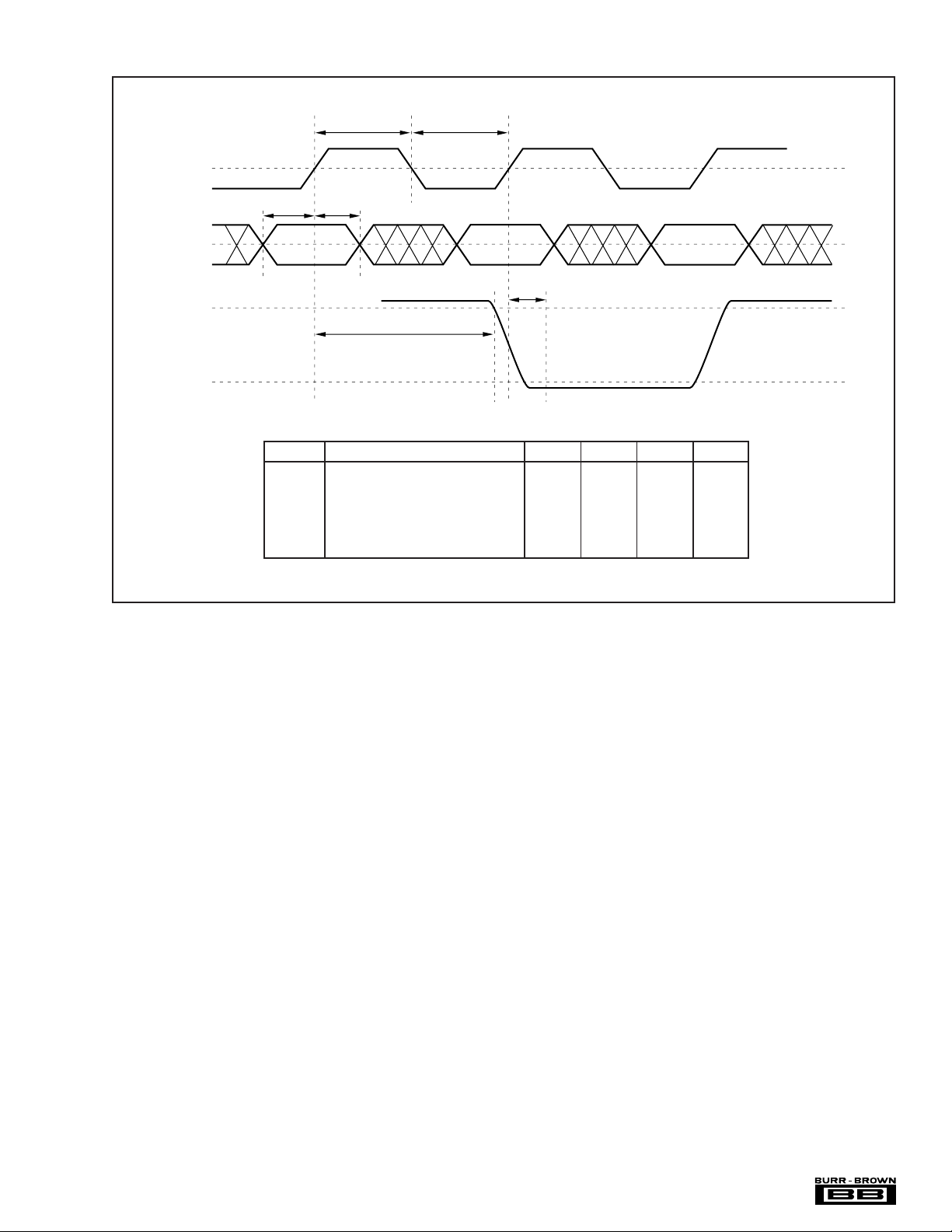
TIMING DIAGRAM
CLK
D13- D0
I
OUT
t
1
t
t
S
H
t
PD
t
2
t
SET
SYMBOL DESCRIPTION MIN TYP MAX UNITS
t
1
t
2
t
S
t
H
t
PD
t
SET
Clock Pulse High Time 6.25 ns
Clock Pulse Low Time 6.25 ns
Data Setup Time 2 ns
Data Hold Time 2 ns
Propagation Delay Time (t1+t2)+1 ns
Output Settling Time to 0.1% 25 ns
®
5
DAC904
 Loading...