

Burr Brown Corporation DAC813KU-1K, DAC813KU, DAC813KP, DAC813JU-1K, DAC813AU-1K Datasheet
...
1
®
DAC813
25kΩ
25kΩ
24.9kΩ
BPO
20V Span
20V Span
V
OUT
V
REF IN
V
REF OUT
10V
Reference
12-Bit D/A
Converter
D/A Latch
Input Latch Input Latch
Reset 4 MSBs 8 LSBs
49.5kΩ
48
12
®
International Airport Industrial Park • Mailing Address: PO Box 11400, Tucson, AZ 85734 • Street Address: 6730 S. Tucson Blvd., Tucson, AZ 85706 • Tel: (520) 746-1111 • Twx: 910-952-1111
Internet: http://www.burr-brown.com/ • FAXLine: (800) 548-6133 (US/Canada Only) • Cable: BBRCORP • Telex: 066-6491 • FAX: (520) 889-1510 • Immediate Product Info: (800) 548-6132
DAC813
DAC813
DAC813
Microprocessor-Compatible
12-BIT DIGITAL-TO-ANALOG CONVERTER
FEATURES
● ±1/2LSB NONLINEARITY OVER
TEMPERATURE
● GUARANTEED MONOTONIC OVER
TEMPERATURE
● LOW POWER: 270mW typ
● DIGITAL INTERFACE DOUBLE
BUFFERED: 12 AND 8 + 4 BITS
● SPECIFIED AT
±12V AND ±15V POWER
SUPPLIES
● RESET FUNCTION TO BIPOLAR ZERO
● 0.3" WIDE DIP AND SO PACKAGES
DESCRIPTION
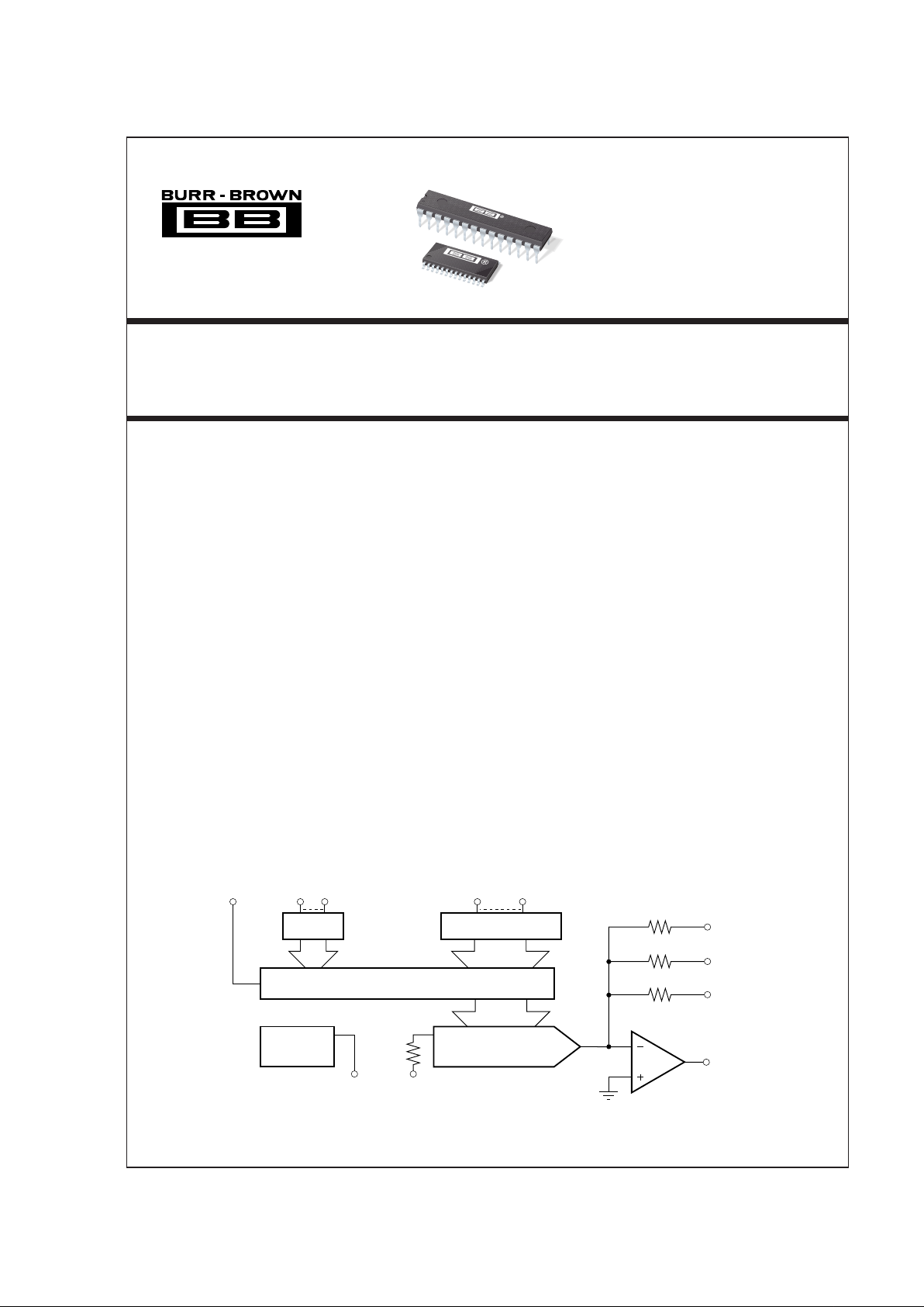
The DAC813 is a complete monolithic 12-bit digitalto-analog converter with a flexible digital interface.
It includes a precision +10V reference, interface control logic, double-buffered latch and a 12-bit D/A
converter with voltage output operational amplifier.
Fast current switches and laser-trimmed thin-film
resistors provide a highly accurate, fast D/A converter.
Digital interfacing is facilitated by a double buffered
latch. The input latch consists of one 8-bit byte and
one 4-bit nibble to allow interfacing to 8-bit (right
justified format) or 16-bit data buses. Input gating
logic is designed so that the last nibble or byte to be
loaded can be loaded simultaneously with the transfer
of data to the D/A latch saving computer instructions.
A reset control allows the DAC813 D/A latch to
asynchronously reset the D/A output to bipolar zero,
a feature useful for power-up reset, recalibration, or
for system re-initialization upon system failure.
The DAC813 is specified to ±1/2LSB maximum linearity error (J, A grades) and ±1/4LSB (K grade).
It is packaged in 28-pin 0.3" wide plastic DIP and
28-lead plastic SOIC
© 1990 Burr-Brown Corporation PDS-1077G Printed in U.S.A. March, 1998
®
2
DAC813
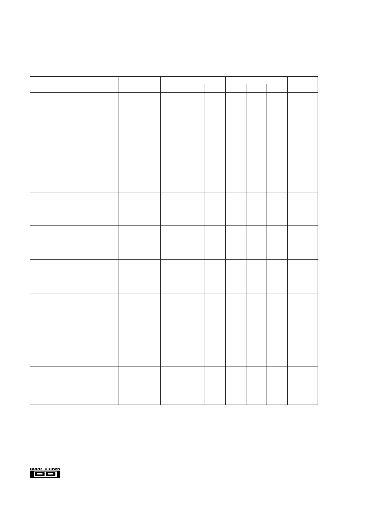
DAC813JP, JU, AU DAC813KP, KU
PARAMETER CONDITIONS MIN TYP MAX MIN TYP MAX UNITS
DIGITAL INPUTS
Resolution 12 ✻ Bits
Codes
(1)
USB, BOB ✻
Digital Inputs Over Temperature Range
(2)
V
IH
(3)
+2 +5.5 ✻✻VDC
V
IL
0 +0.8 ✻✻VDC
DATA Bits, WR, Reset, LDAC, LMSB, LLSB ±10 ✻ µA
I
IH
VIN = +2.7V ±10 ✻ µA
I
IL
VIN = +0.4V
ACCURACY
Linearity Error ±1/4 ±1/2 ±1/8 ±1/4 LSB
Differential Linearity Error ±1/2 ±3/4 ±1/4 ±1/2 LSB
Gain Error
(4)
±0.05 ±0.2 ✻✻ %
Unipolar Offset Error
(5)
±0.01 ±0.02 ✻✻% of FSR
(7)
Bipolar Zero Error
(6)
±0.02 ±0.2 ✻✻% of FSR
Monotonicity Guaranteed ✻
Power Supply Sensitivity: +V
CC
20V Range 5 10 ✻✻ppm of FSR/%
–V
CC
110 ✻✻ppm of FSR/%
DRIFT Over Specification
Gain Temperature Range ±5 ±30 ✻ ±15 ppm/°C
Unipolar Offset ±1 ±3 ✻ ±3 ppm of FSR/°C
Bipolar Zero ±3 ±10 ✻ ±5 ppm of FSR/°C
Linearity Error Over Temperature Range ±1/2 ±3/4 ±1/4 ±1/2 LSB
Monotonicity Over Temperature Range Guaranteed ✻
SETTLING TIME
(8)
(To Within ±0.01% of
FSR of Final Value; 5kΩ || 500pF load)
For Full Scale Range Change 20V Range 4.5 6 ✻✻ µs
10V Range 3.3 5 ✻✻ µs
For 1LSB Change at Major Carry
(9)
2 ✻ µs
Slew Rate 10 ✻ V/µs
ANALOG OUTPUT
Voltage Range: Unipolar ±V
CC
> ±11.4V 0 to +10 ✻ V
Bipolar ±V
CC
> ±11.4V ±5, ±10 ✻ V
Output Current ±5 ✻ mA
Output Impedance At DC 0.2 ✻ Ω
Short Circuit to Common Duration Indefinite ✻
REFERENCE VOLTAGE
Voltage +9.95 +10 +10.05 ✻✻✻ V
Source Current Available for External Loads 5 ✻ mA
Impedance 2 ✻ Ω
Temperature Coefficient ±5 ±25 ✻✻ppm/°C
Short Circuit to Common Duration Indefinite ✻
POWER SUPPLY REQUIREMENTS
Voltage: +V
CC
+11.4 +15 +16.5 ✻✻✻ VDC
–V
CC
–11.4 –15 –16.5 ✻✻✻ VDC
Current: +V
CC
+ V
L
No Load 13 15 ✻✻ mA
–V
CC
No Load –5 –7 ✻✻ mA
Potential at DCOM with Respect to ACOM
(10)
–3 +3 ✻✻V
Power Dissipation 270 330 ✻✻ mW
TEMPERATURE RANGE
Specification: J, K 0 +70 ✻✻°C
A –40 +85 ✻✻°C
Operating: J, K –40 +85 ✻✻°C
A –55 +125 ✻✻°C
Storage: J, K –60 +100 ✻✻°C
A –65 +150 ✻✻°C
✻ Same as specification for DAC813AU, JP, JU.
NOTES: (1) USB = Unipolar Straight Binary; BOB = Bipolar Offset Binary. (2) TTL and 5V CMOS compatible. (3) Open DATA input lines will be pulled above +5.5V.
See discussion under LOGIC INPUT COMPATIBILITY in the OPERATION section. (4) Specified with 500Ω Pin 6 to 7. Adjustable to zero with external trim
potentiometer. (5) Error at input code 000
HEX
for unipolar mode, FSR = 10V. (6) Error at input code 800
HEX
for bipolar range. Specified with 100Ω Pin 6 to 4 and
with 500Ω pin 6 to 7. See page 9 for zero adjustment procedure. (7) FSR means Full Scale Range and is 20V for the ±10V range. (8) Maximum represents the
3σ limit. Not 100% tested for this parameter. (9) At the major carry, 7FF
HEX
to 800
HEX
and 800
HEX
to 7FF
HEX
. (10) The maximum voltage at which ACOM and DCOM
may be separated without affecting accuracy specifications.
SPECIFICATIONS
At TA = +25°C, ±VCC = ±12V or ±15V and load on V
OUT
= 5kΩ || 500pF to common, unless otherwise noted.
3
®
DAC813
The information provided herein is believed to be reliable; however, BURR-BROWN assumes no responsibility for inaccuracies or omissions. BURR-BROWN assumes
no responsibility for the use of this information, and all use of such information shall be entirely at the user’s own risk. Prices and specifications are subject to change
without notice. No patent rights or licenses to any of the circuits described herein are implied or granted to any third party. BURR-BROWN does not authorize or warrant
any BURR-BROWN product for use in life support devices and/or systems.
+V
CC
to ACOM .......................................................................... 0 to +18V
–V
CC
to ACOM .......................................................................... 0 to –18V
+V
CC
to –VCC............................................................................ 0 to +36V
DCOM with respect to ACOM ............................................................. ±4V
Digital Inputs (Pins 11–15, 17–28) to DCOM ....................–0.5V to +V
CC
External Voltage Applied to BPO Span Resistor .............................. ±V
CC
V
REF OUT
........................................................... Indefinite Short to ACOM
V
OUT
................................................................. Indefinite Short to ACOM
Power Dissipation .......................................................................... 750mW
Lead Temperature (soldering, 10s) ............................................... +300°C
Max Junction Temperature ............................................................ +165°C
Thermal Resistance,
θ
J-A
:Plastic DIP and SOIC ........................130°C/W
Ceramic DIP......................................... 85 °C/W
NOTE: (1) Stresses above those listed under “Absolute Maximum Ratings”
may cause permanent damage to the device. Exposure to absolute maximum
conditions for extended periods may affect device reliability.
ABSOLUTE MAXIMUM RATINGS
(1)
PIN NAME DESCRIPTION
1+V
L
Positive supply pin for logic circuits. Connect to +VCC.
2, 3 20V Range Connect Pin 2 or Pin 3 to Pin 9 (V
OUT
) for a 20V
FSR. Connect both to Pin 9 for a 10V FSR.
4 BPO Bipolar offset. Connect to Pin 6 (V
REF OUT
) through
100Ω resistor or 200Ω potentiometer for bipolar
operation.
5 ACOM Analog common, ±V
CC
supply return.
6V
REF OUT
+10V reference output referred to ACOM.
7V
REF IN
Connected to V
REF OUT
through a 1kΩ gain
adjustment potentiometer or a 500Ω resistor.
8+V
CC
Analog supply input, nominally +12V to +15V
referred to ACOM.
9V
OUT
D/A converter voltage output.
10 –V
CC
Analog supply input, nominally –12V or –15V
referred to ACOM.
11 WR Master enable for LDAC, LLSB, and LMSB. Must
be low for data transfer to any latch.
12 LDAC Load DAC. Must be low with WR for data transfer
to the D/A latch and simultaneous update of the
D/A converter.
13 Reset When low, resets the D/A latch such that a Bipolar
Zero output is produced. This control overrides all
other data input operations.
14 LMSB Enable for 4-bit input latch of D
8-D11
data inputs.
NOTE: This logic path is slower than the WR path.
15 LLSB Enable for 8-bit input latch of D
0-D7
data inputs.
NOTE: This logic path is slower than the WR path.
16 DCOM Digital common.
17 D0 Data Bit 1, LSB.
18 D1 Data Bit 2.
19 D2 Data Bit 3.
20 D3 Data Bit 4.
21 D4 Data Bit 5.
22 D5 Data Bit 6.
23 D6 Data Bit 7.
24 D7 Data Bit 8.
25 D8 Data Bit 9.
26 D9 Data Bit 10.
27 D10 Data Bit 11.
28 D11 Data Bit 12, MSB, positive true.
PIN DESCRIPTIONS
ELECTROSTATIC
DISCHARGE SENSITIVITY
Electrostatic discharge can cause damage ranging from performance degradation to complete device failure. BurrBrown Corporation recommends that all integrated circuits
be handled and stored using appropriate ESD protection
methods.
ESD damage can range from subtle performance degradation to complete device failure. Precision integrated circuits
may be more susceptible to damage because very small
parametric changes could cause the device not to meet
published specifications.
PACKAGE/ORDERING INFORMATION
PACKAGE LINEARITY GAIN
DRAWING TEMPERATURE ERROR, MAX DRIFT
PRODUCT PACKAGE NUMBER
(1)
RANGE AT +25°C (LSB) (ppm/°C)
DAC813JP 28-Pin Plastic DIP 246 0°C to +70°C ±1/2 ±30
DAC813JU 28-Lead Plastic SOIC 217 0°C to +70°C ±1/2 ±30
DAC813KP 28-Pin Plastic DIP 246 0°C to +70°C ±1/4 ±15
DAC813KU 28-Lead Plastic SOIC 217 0°C to +70°C ±1/4 ±15
DAC813AU 28-Lead Plastic SOIC 217 –40°C to +85°C ±1/2 ±30
NOTE: (1) For detailed drawing and dimension table, please see end of data sheet, or Appendix C of Burr-Brown IC Data Book.

®
4
DAC813
MINIMUM TIMING DIAGRAMS
WRITE CYCLE #1
>5ns
> 50ns
> 50ns
(Load first rank from Data Bus: LDAC = 1)
DB11–DB0
WR
LLSB, LMSB
> 50ns
WRITE CYCLE #2
t
SETTLING
(Load second rank from first rank: LLSB, LMSB = 1)
WR
±1/2LSB
LDAC
> 50ns
> 50ns
RESET COMMAND (Bipolar Mode)
±1/2LSB
Reset
> 50ns
+10V
–10V
0V
t
SETTLING
V
OUT
LLSB, LMSB, LDAC, WR = Don’t Care
 Loading...