

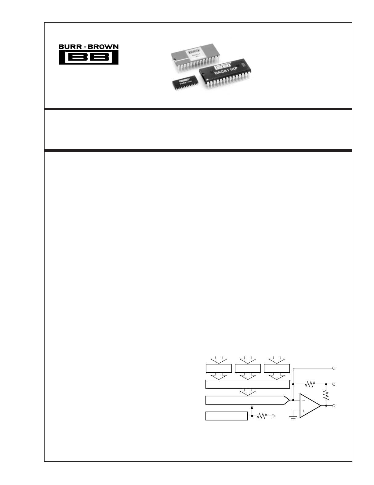
Burr Brown Corporation DAC811KU, DAC811KP, DAC811JU-1K, DAC811JU, DAC811JP Datasheet
...
®
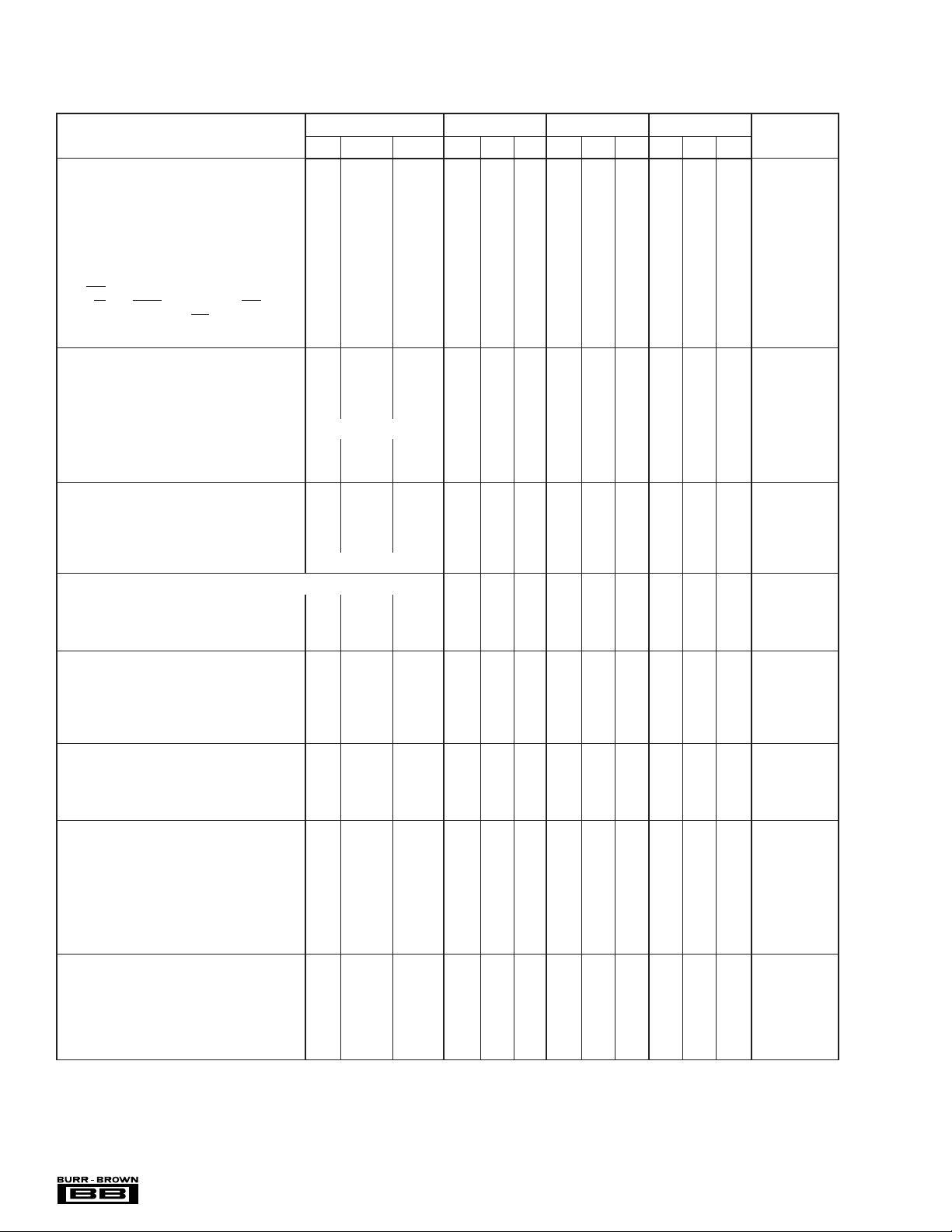
BPO
V
OUT
D/A Latch
Input Latch
4 MSBs
Input Latch Input Latch
4 LSBs
12-Bit D/A Converter
Voltage Reference
10V
R
F
S
J
R
F
R
BPO
For most current data sheet and other product
information, visit www.burr-brown.com
Microprocessor-Compatible
12-BIT DIGITAL-TO-ANALOG CONVERTER
DAC811
FEATURES
● SINGLE INTEGRATED CIRCUIT CHIP
● MICROCOMPUTER INTERFACE:
DOUBLE-BUFFERED LATCH
● VOLTAGE OUTPUT: ±10V, ±5V, +10V
● MONOTONICITY GUARANTEED OVER
TEMPERATURE
● ±1/2LSB MAXIMUM NONLINEARITY OVER
TEMPERATURE
● GUARANTEED SPECIFICATIONS AT ±12V
AND ±15V SUPPLIES
● TTL/5V CMOS-COMPATIBLE LOGIC
INPUTS
Input gating logic is designed so that loading the last
nibble or byte of data can be accomplished simultaneously with the transfer of data (previously stored in
adjacent latches) from adjacent input latches to the
D/A latch. This feature avoids spurious analog output
values while using an interface technique that saves
computer instructions.
The DAC811 is laser trimmed at the wafer level and
is specified to ±1/4LSB maximum linearity error (B,
K, and S grades) at 25°C and ±1/2LSB maximum over
the temperature range. All grades are guaranteed monotonic over the specification temperature range.
The DAC811 is available in six performance grades
and three package types. DAC811J and K are specified over the temperature ranges of 0°C to +70°C;
DAC811A and B are specified over –25°C to +85°C;
DAC811R and S are specified over –55°C to +125°C.
DESCRIPTION
The DAC811 is a complete, single-chip integratedcircuit, microprocessor-compatible, 12-bit digital-toanalog converter. The chip combines a precision voltage reference, microcomputer interface logic, and
DAC811J and K are packaged in a reliable 28-pin
plastic DIP or plastic SOIC package, while DAC811A,
B, R and S are available in a 28-pin 0.6" wide dualinline hermetically sealed ceramic side-brazed package (H package).
double-buffered latch, in a 12-bit D/A converter with
a voltage output amplifier. Fast current switches and a
laser-trimmed thin-film resistor network provide a
highly accurate and fast D/A converter.
Microcomputer interfacing is facilitated by a doublebuffered latch. The input latch is divided into three
4-bit nibbles to permit interfacing to 4-, 8-, 12-, or
16-bit buses and to handle right-or left-justified data.
The 12-bit data in the input latches is transferred to the
D/A latch to hold the output value.
International Airport Industrial Park • Mailing Address: PO Box 11400, Tucson, AZ 85734 • Street Address: 6730 S. Tucson Blvd., Tucson, AZ 85706 • Tel: (520) 746-1111
Twx: 910-952-1111 • Internet: http://www.burr-brown.com/ • Cable: BBRCORP • Telex: 066-6491 • FAX: (520) 889-1510 • Immediate Product Info: (800) 548-6132
© 1983 Burr-Brown Corporation PDS-503K Printed in U.S.A. January, 2000
1
DAC811
®
SPECIFICATIONS
At TA = +25°C. ±VCC = 12V or 15V, unless otherwise noted.
DAC811AH, JP, JU DAC811BH, KP, KU
DAC811RH DAC811SH
PARAMETER MIN TYP MAX MIN TYP MAX MIN TYP MAX MIN TYP MAX UNITS
DIGITAL INPUT
Resolution 12 ✻✻✻Bits
(1)
Codes
Digital Inputs Over Temperature Range
V
IH
V
IL
I
, VI = +2.7V +10 ✻✻✻µA
IH
I
, VI = +0.4V ±20 ✻✻✻µA
IL
Digital Interface Timing Over Temperature Range
(2)
USB, BOB
✻✻✻
+2 +15 ✻✻✻✻✻✻VDC
0 +0.8 ✻✻✻✻✻✻VDC
tWP, WR Pulse Width 50 ✻✻✻ ns
t
1, NX and LDAC Valid to End of WR 50 ✻✻✻
AW
, Data Valid to End of WR 80 ✻✻✻ ns
DW
t
, Data Valid Hold Time 0 ✻ +10 ✻ ns
DH
nst
ACCURACY
Linearity Error ±1/4 ±1/2 ±1/8 ±1/4 ±1/4 ±1/2 ±1/8 ±1/4 LSB
Differential Linearity Error ±1/2 ±3/4 ±1/4 ±1/2 ±1/2 ±3/4 ±1/4 ±1/2 LSB
Gain Error
Offset Error
(3)
(3, 4)
±0.1 ±0.2 ✻✻ ✻✻ ✻✻ %
±0.05 ±0.15 ✻✻ ✻✻ ✻✻ % of FSR
(5)
Monotonicity Guaranteed ✻✻✻
Power Supply Sensitivity: +V
–V
CC
V
DD
CC
±0.001 ±0.003 ✻✻ ✻✻ ✻ ✻% of FSR/%V
±0.002 ±0.006 ✻✻ ✻✻ ✻ ✻% of FSR/%V
±0.0005 ±0.0015 ✻✻ ✻✻ ✻✻% of FSR/%V
CC
CC
DD
DRIFT (Over Specification Temperature Range)
Gain ±10 ±30 ±10 ±20 ±15 ±30 ±15 ±30 ppm/°C
Unipolar Offset ±5 ±10 ±5 ±7 ±5 ±10 ±5 ±7 ppm of FSR/°C
Bipolar Zero ±5 ±10 ±5 ±7 ±5 ±10 ±5 ±7 ppm of FSR/°C
Linearity Error Over Temperature Range ±1/2 ±3/4 ±1/4 ±1/2 ±1/2 ±3/4 ±1/4 ±1/2 LSB
Monotonicity Over Temperature Range Guaranteed ✻✻✻
SETTLING TIME
(6)
(to within ±0.01% of FSR of Final Value; 2kΩ load)
For Full Scale Range Change, 20V Range 3 4 ✻✻ ✻✻ ✻✻ µs
10V Range 3 4 ✻✻ ✻✻ ✻✻ µs
For 1LSB Change at Major Carry
Slew Rate
(6)
ANALOG OUTPUT
Voltage Range (±V
Bipolar ±5, ±10 ✻✻✻V
= 15V)
CC
(7)
1 ✻✻✻µs
812 ✻✻ ✻✻ ✻✻ V/µs
(8)
: Unipolar 0 to +10 ✻✻✻V
Output Current ±5 ✻✻✻ mA
Output Impedance (at DC) 0.2 ✻✻✻Ω
Short Circuit to Common Duration Indefinite ✻✻✻
REFERENCE VOLTAGE
Voltage +6.2 +6.3 +6.4 ✻✻✻✻✻✻✻✻✻ V
Source Current Available for External Loads +2 ✻✻✻ mA
Temperature Coefficient ±10 ±30 ±10 ±20 ±10 ±30 ±10 ±20 ppm/°C
Short Circuit to Common Duration Indefinite ✻✻✻
POWER SUPPLY REQUIREMENTS
Voltage: +V
–V
V
DD
Current (no load): +V
–V
V
DD
Potential at DCOM with Respect to ACOM
CC
CC
CC
CC
+11.4 +15 +16.5 ✻✻✻✻✻✻✻✻✻ VDC
–11.4 –15 –16.5 ✻✻✻✻✻✻✻✻✻ VDC
+4.5 +5 +5.5 ✻✻✻✻✻✻✻✻✻ VDC
+16 +25 ✻✻ ✻✻ ✻✻ mA
–23 –35 ✻✻ ✻✻ ✻✻ mA
(9)
+8 +15 ✻✻ ✻✻ ✻✻ mA
±0.5 ✻✻✻V
Power Dissipation 625 800 ✻✻ ✻✻ ✻✻ mW
TEMPERATURE RANGE
Specification: J, K 0 +70 ✻✻✻✻✻✻°C
A, B –25 +85 ✻✻✻✻✻✻°C
R, S –65 +150 ✻✻✻✻✻✻°C
–55 +125 ✻✻°C
Storage: J, K –60 +100 ✻✻✻✻✻✻°C
A, B, R, S –65 +150 ✻✻✻✻✻✻°C
✻ Specification same as DAC811AH.
NOTES: (1) USB = unipolar straight binary; BOB = bipolar offset binary. (2) TTL, LSTTL and 54/74 HC compatible. (3) Adjustable to zero with external trim
potentiometer. (4) Error at input code 000
represents the 3σ limit. Not 100% tested for this parameter. (7) At the major carry, 7FF
output swing is ±13.5V. Output swing for ±11.4V supplies is at least –8V to +8V. (9) The maximum voltage at which ACOM and DCOM may be separated without
for both unipolar and bipolar ranges. (5) FSR means full scale range and is 20V for the ±10V range. (6) Maximum
16
to 80016 and 80016 to 7FF16. (8) Minimum supply voltage required for ±10V
16
affecting accuracy specifications.
®
DAC811
2
PIN DESCRIPTIONS
PIN
NAME FUNCTION
1+V
DD
2 WR Write, command signal to load latches. Logic low
3 LDAC Load D/A converter, enables WR to load the D/A
4N
A
5N
B
6N
C
7D
11
8D
10
9D
9
10 D
8
11 D
7
12 D
6
13 D
5
14 D
4
15 DCOM Digital common, V
16 D
0
17 D
1
18 D
2
19 D
3
20 +V
CC
21 –V
CC
22 Gain Adj To externally adjust gain.
23 ACOM Analog common, ±V
24 V
OUT
25 10V Range Connect to pin 24 for 10V range.
26 SJ Summing junction of output amplifier.
27 BPO Bipolar offset. Connect to pin 26 for bipolar
28 Ref Out 6.3V reference output.
Logic supply, +5V.
loads latches.
latch. Logic low enables.
Nibble A, enables WR to load input latch A (the
most significant nibble). Logic low enables.
Nibble B, enables WR to load input latch B. Logic
low enables.
Nibble C, enables WR to load input latch C (the
least significant nibble). Logic low enables.
Data bit 12, MSB, positive true.
Data bit 11.
Data bit 10.
Data bit 9.
Data bit 8.
Data bit 7.
Data bit 6.
Data bit 5.
supply return.
Data bit 1, LSB.
Data bit 2.
Data bit 3.
Data bit 4.
Analog supply input, +15V or +12V.
Analog supply input, –15V or –12V.
D/A converter voltage output.
operation.
DD
supply return.
CC
ABSOLUTE MAXIMUM RATINGS
+V
................................................................................................................................ 0 to +18V
CC
–V
to ACOM .......................................................................... 0 to –18V
CC
V
to DCOM .............................................................................. 0 to +7V
DD
V
to ACOM ......................................................................................±7V
DD
ACOM to DCOM .................................................................................. ±7V
Digital Inputs (Pins 2–14, 16–19) to DCOM ......................–0.4V to +18V
External Voltage Applied to 10V Range Resistor ............................ ±12V
Ref Out ............................................................. Indefinite Short to ACOM
External Voltage Applied to DAC Output ................................ –5V to +5V
Power Dissipation ........................................................................ 1000mW
Lead Temperature (soldering, 10s) ............................................... +300°C
Max Junction Temperature ............................................................ +165°C
Thermal Resistance,
Ceramic DIP .................................................................................. 65°C/W
NOTE: Stresses above those listed above may cause permanent damage to
the device. Exposure to absolute maximum conditions for extended periods
may affect device reliability.
θ
: Plastic DIP and SOIC ....................... 100°C/W
J-A
ELECTROSTATIC
DISCHARGE SENSITIVITY
This integrated circuit can be damaged by ESD. Burr-Brown
recommends that all integrated circuits be handled with
appropriate precautions. Failure to observe proper handling
and installation procedures can cause damage.
ESD damage can range from subtle performance degradation
to complete device failure. Precision integrated circuits may
be more susceptible to damage because very small parametric
changes could cause the device not to meet its published
specifications.
PACKAGE/ORDERING INFORMATION
MINIMUM
RELATIVE DIFFERENTIAL PACKAGE SPECIFICATION
PRODUCT (LSB) (LSB) PACKAGE NUMBER RANGE NUMBER
ACCURACY LINEARITY DRAWING TEMPERATURE ORDERING TRANSPORT
DAC811AH ±1/2 LSB 3/4 CerDIP-28 149 –25°C to +85°C DAC811AH Rails
DAC811JP ±1/2 LSB 3/4 DIP-28 215 0°C to +70°C DAC811JP Rails
DAC811JU ±1/2 LSB 3/4 SOIC-28 217 0°C to +70°C DAC811JU Rails
"" """ "DAC811JU/1K Tape and Reel
DAC811KP ±1/4 LSB 1/2 DIP-28 215 0°C to +70°C DAC811KP Rails
DAC811KU ±1/4 LSB 1/2 SOIC-28 217 0°C to +70°C DAC811KU Rails
NOTE: (1) Models with a slash (/) are available only in Tape and Reel in the quantities indicated (e.g., /1K indicates 1000 devices per reel). Ordering 1000 pieces
of “DAC811JU/1K” will get a single 1000-piece Tape and Reel.
The information provided herein is believed to be reliable; however, BURR-BROWN assumes no responsibility for inaccuracies or omissions. BURR-BROWN assumes
no responsibility for the use of this information, and all use of such information shall be entirely at the user’s own risk. Prices and specifications are subject to change
without notice. No patent rights or licenses to any of the circuits described herein are implied or granted to any third party. BURR-BROWN does not authorize or warrant
any BURR-BROWN product for use in life support devices and/or systems.
(1)
MEDIA
®
3
DAC811
 Loading...