Burr Brown Corporation DAC8043UC, DAC8043U Datasheet

®
12-Bit
D/A
Converter
12-Bit
DAC Register
12-Bit Input
Shift Register
12
12
V
REF
LD
CLK
SRI
R
FB
I
OUT
V
DD
GND
1
5
7
6
2
3
8
4
R
FB
DAC8043
DAC8043
CMOS 12-Bit Serial Input Multiplying
DIGITAL-TO-ANALOG CONVERTER
FEATURES
● 12-BIT ACCURACY IN 8-PIN SOIC
● FAST 3-WIRE SERIAL INTERFACE
● LOW INL AND DNL:
● GAIN ACCURACY TO
● LOW GAIN TEMPCO: 5ppm/
● OPERATES WITH +5V SUPPLY
±1/2 LSB max
±1LSB max
°C max
APPLICATIONS
● AUTOMATIC CALIBRATION
● MOTION CONTROL
● MICROPROCESSOR CONTROL SYSTEMS
● PROGRAMMABLE AMPLIFIER/
ATTENUATORS
● DIGITALLY CONTROLLED FILTERS
● TTL/CMOS COMPATIBLE
● ESD PROTECTED
DESCRIPTION
The DAC8043 is a 12-bit current output multiplying
digital-to-analog converter (DAC) that is packaged in a
space-saving, surface-mount 8-pin SOIC. Its 3-wire serial interface saves additional circuit board space which
results in low power dissipation. When used with microprocessors having a serial port, the DAC8043 minimizes
the digital noise feedthrough from its input to output.
The serial port can be used as a dedicated analog bus and
kept inactive while the DAC8043 is in use. Serial interfacing reduces the complexity of opto or transformer
isolation applications.
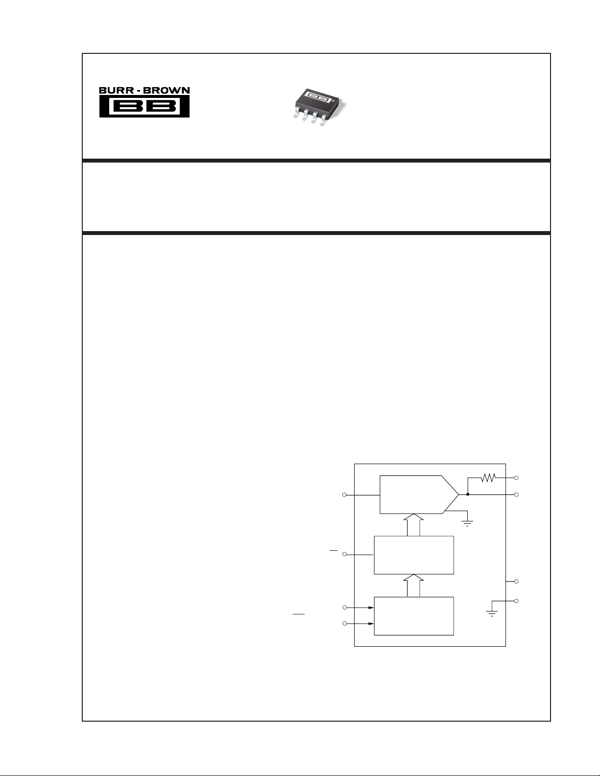
The DAC8043 contains a 12-bit serial-in, parallel-out
shift register, a 12-bit DAC register, a 12-bit CMOS
DAC, and control logic. Serial input (SRI) data is clocked
into the input register on the rising edge of the clock
(CLK) pulse. When the new data word had been clocked
in, it is loaded into the DAC register by taking the LD
input low. Data in the DAC register is converted to an
output current by the D/A converter.
The DAC8043 operates from a single +5V power supply
which makes the DAC8043 an ideal low power, small
size, high performance solution for several applications.
International Airport Industrial Park • Mailing Address: PO Box 11400, Tucson, AZ 85734 • Street Address: 6730 S. Tucson Blvd., Tucson, AZ 85706 • Tel: (520) 746-1111 • Twx: 910-952-1111
Internet: http://www.burr-brown.com/ • FAXLine: (800) 548-6133 (US/Canada Only) • Cable: BBRCORP • Telex: 066-6491 • FAX: (520) 889-1510 • Immediate Product Info: (800) 548-6132
©
1993 Burr-Brown Corporation PDS-1197B Printed in U.S.A. March, 1998
1
DAC8043
®

SPECIFICATIONS
ELECTRICAL CHARACTERISTICS
At VDD = +5V; V
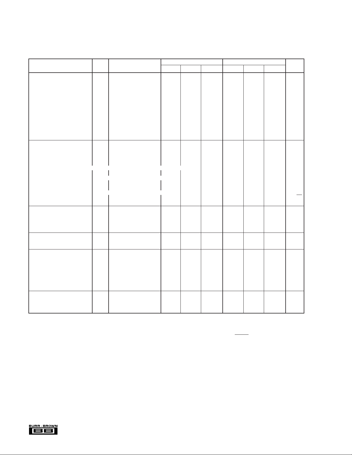
PARAMETER SYMBOL CONDITIONS MIN TYP MAX MIN TYP MAX UNITS
STATIC PERFORMANCE
Resolution N 12 12 Bits
Nonlinearity
Differential Nonlinearity
Gain Error
Gain Tempco
Power Supply Rejection Ratio PSRR ∆V
Output Leakage Current
Zero Scale Error
Input Resistance
AC PERFORMANCE
Output Current Settling Time
Digital-to-Analog Glitch V
Energy
Feedthrough Error
(V
to I
REF
Total Harmonic Distortion
Output Noise Voltage Density
DIGITAL INPUTS
Digital Input High V
Digital Input Low V
Input Leakage Current
Input Capacitance
ANALOG OUTPUTS
Output Capacitance
TIMING CHARACTERISTICS
Data Setup Time tDSTA = Full Temperature Range 40 40 ns
Data Hold Time t
Clock Pulse Width High t
Clock Pulse Width Low t
Load Pulse Width t
LSB Clock into Input Register
to Load DAC Register Time t
POWER SUPPLY
Supply Voltage V
Supply Current I
NOTES: (1) ±1/2 LSB = ±0.012% of Full Scale. (2) All grades are monotonic to 12-bits over temperature. (3) Using internal feedback resistor. (4) Applies to I
digital inputs = 0V. (5) Guaranteed by design and not tested. (6) I
t
= propagation delay (tPD) + 9τ where τ = measured time constant of the final RC decay. (7) V
S
is less than ±50ppm/°C. (9) Digital inputs are CMOS gates: I
inputs = 0V. (12) Calculated from worst case R
J/°K, R = resistance, Ω. T = Resistor temperature, °K, B = bandwidth, Hz. (14) Tested at V
= +10V; I
REF
(1)
(3)
(5)
(7, 12)
(8)
(5, 10)
(5, 11)
) Digital Input = 0000 0000 0000
OUT
(5, 11)
= GND = 0V; TA = Full Temperature Range specified under Absolute Maximum Ratings, unless otherwise noted.
OUT
(2)
INL ±1 ±1/2 LSB
DNL ±1 ±1/2 LSB
FSE TA = +25°C ±2 ±1 LSB
T
= Full Temp Range ±2 ±2 LSB
TC
FSE
(4)
(5, 6)
I
LKG
I
ZSE
R
IN
t
S
QI
DAC Register Loaded Alternately with all 0s and all 1s
FT V
(5)
(9)
(5)
(5, 13)
(5, 14)
THD V
e
N
IH
IL
I
IL
C
IN
C
OUT
DHTA
CHTA
CLTA
LDTA
ASBTA
DD
DD
A
= ±5% ±0.0006 ±0.002 ±0.0006 ±0.002 %/%
DD
TA = +25°C ±5 ±5nA
T
= Full Temp Range ±100 ±25 nA
A
TA = +25°C 0.03 0.03 LSB
T
= Full Temp Range 0.60 0.15 LSB
A
TA = +25°C 0.25 1 0.25 1 µs
= 0V 2 20 2 20 nVs
REF
= Load = 100Ω
OUT
C
= 13pF
EXT
= 20Vp-p at f = 10kHz 0.7 1 0.7 1 mVp-p
REF
T
= +25°C
A
= 6V
REF
DAC Register Loaded with all 1s
at 1kHz –85 –85 dB
RMS
10Hz to 100kHz 17 17 nV/√Hz
Between R
FB
and I
VIN = 0V to +5V ±1 ±1 µA
VIN = 0V 8 8 pF
Digital Inputs = V
Digital Inputs = V
= Full Temperature Range 80 80 ns
= Full Temperature Range 90 90 ns
= Full Temperature Range 120 120 ns
= Full Temperature Range 120 120 ns
= Full Temperature Range 0 0 ns
Digital Inputs = VIH or V
Digital Inputs = 0V or V
is typically 1nA at +25°C. (10) V
(in LSBs) = (R
ZSE
IN
: I
REF
OUT
IH
IL
IL
DD
Load = 100Ω, C
OUT
X I
X 4096)/V
REF
LKG
DAC8043U DAC8043UC
±5 ±5 ppm/°C
7 11 15 7 11 15 kΩ
2.4 2.4 V
0.8 0.8 V
110 110 pF
80 80 pF
4.75 5 5.25 4.75 5 5.25 V
500 500 µA
100 100 µA
= 13pF, digital input = 0V to VDD or VDD to 0V. Extrapolated to 1/2 LSB:
EXT
= +10V, all digital inputs = 0V. (8) Absolute temperature coefficient
REF
= 0V, all digital inputs = 0V to VDD or VDD to 0V. (11) All digital
REF
. (13) Calculations from en = √4K TRB where: K = Boltzmann constant,
REF
= 0V or VDD.
IN
OUT
; All
The information provided herein is believed to be reliable; however, BURR-BROWN assumes no responsibility for inaccuracies or omissions. BURR-BROWN assumes
no responsibility for the use of this information, and all use of such information shall be entirely at the user’s own risk. Prices and specifications are subject to change
without notice. No patent rights or licenses to any of the circuits described herein are implied or granted to any third party. BURR-BROWN does not authorize or warrant
any BURR-BROWN product for use in life support devices and/or systems.
®
DAC8043
2

WAFER TEST LIMITS
At VDD = +5V; V
REF
= +10V; I
= GND = 0V; TA = +25°C.
OUT
PARAMETER SYMBOL CONDITIONS LIMIT UNITS
STATIC ACCURACY
Resolution N 12 Bits min
Integral Nonlinearity INL ±1 LSB max
Differential Nonlinearity DNL ±1 LSB max
Gain Error G
Power Supply Rejection Ratio PSRR ∆V
Output Leakage Current (I
REFERENCE INPUT
Input Resistance R
DIGITAL INPUTS
Digital Input HIGH V
Digital Input LOW V
Input Leakage Current I
POWER SUPPLY
Supply Current I
NOTE: Electrical tests are performed at wafer probe to the limits shown. Due to variations in assembly methods and normal yield loss, yield after packaging is not
guaranteed for standard product dice. Consult factory to negotiate specifications based on dice lot qualifications through sample lot assembly and testing.
)I
OUT
FSE
LKG
IN
IH
IL
IL
DD
ABSOLUTE MAXIMUM RATINGS
VDD to GND .................................................................................. 0V, +7V
V
to GND ...................................................................................... ±25V
REF
V
to GND ...................................................................................... ±25V
RFB
Digital Input Voltage Range ................................................. –0.3V to V
Output Voltage (Pin 3) ......................................................... –0.3 V to V
Operating Temperature Range
AD ........................................................................................0°C to +70°C
U, UC ............................................................................... –40°C to +85°C
Junction Temperature.................................................................... +150°C
Storage Temperature .................................................... –65°C to + 150°C
Lead Temperature (soldering, 10s).............................................. +300° C
θ
..........................................................................................................................
JA
θ
...........................................................................................+42°C/W
JC
CAUTION: 1. Do not apply voltages higher than V
potential on any terminal except V
control inputs are ESD protected: however, permanent damage may occur on
unprotected units from high-energy electrostatic fields. Keep units in conductive foam at all times until ready to use. 3. Use proper anti-static handling
procedures. 4. Absolute Maximum Ratings apply to both packaged devices.
Stresses above those listed under Absolute Maximum Ratings may cause
permanent damage to the device.
(Pin 1) and R
REF
or less than GND
DD
(Pin 2). 2. The digital
FB
Using Internal Feedback Resistor ±2 LSB max
Digital Inputs = VIH or V
Digital Inputs = 0V to V
= ±5% ±0.002 %/% max
DD
Digital Inputs = V
VIN = 0V to V
IL
DD
IL
DD
±5 nA max
7/15 kΩ min/max
2.4 V min
0.8 V max
±1 µA max
500 µA max
100 µA max
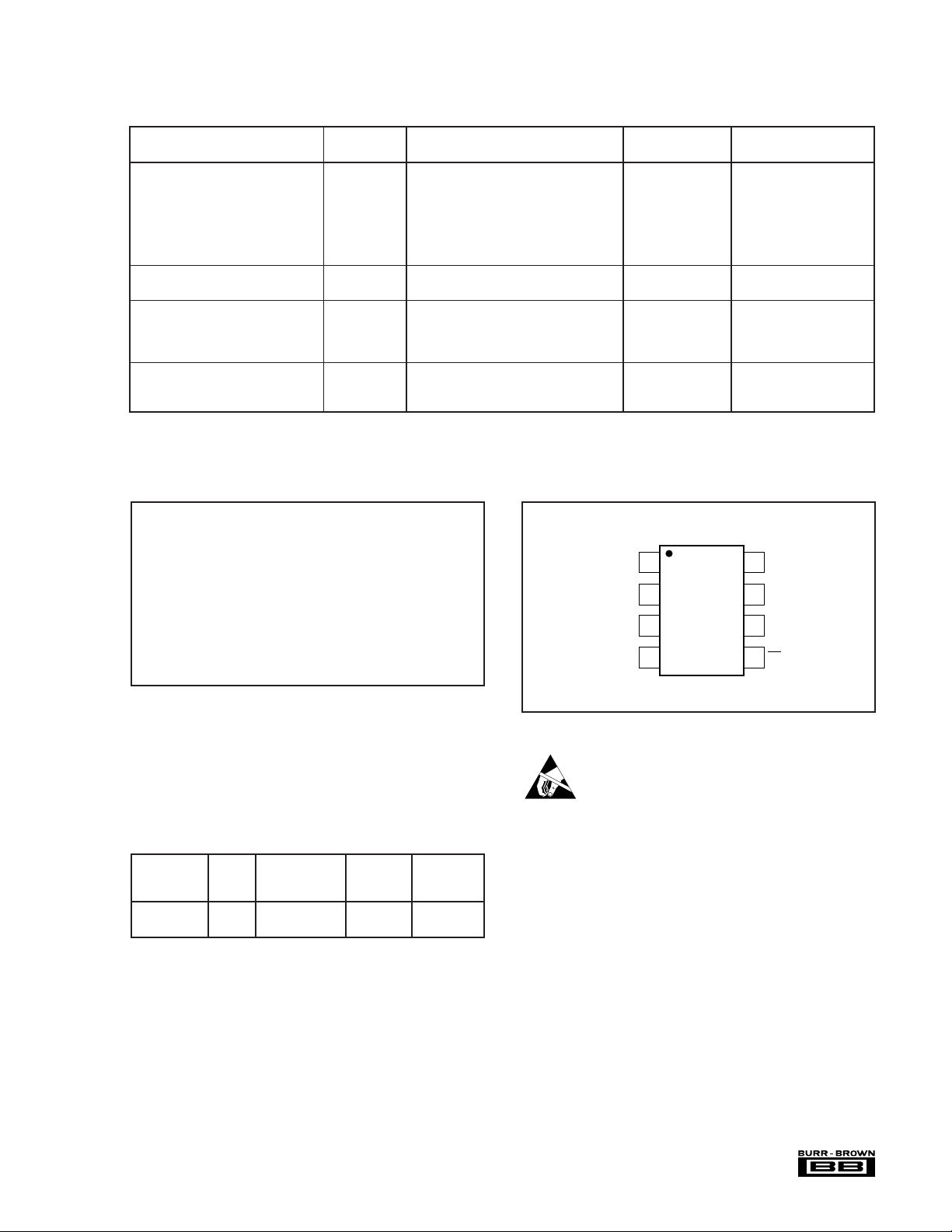
PIN CONFIGURATION
Top View 8-Pin SOIC
DD
DD
+100°C/W
V
REF
R
I
OUT
GND
1
2
FB
3
4
ELECTROSTATIC
DISCHARGE SENSITIVITY
DAC8043
V
8
DD
7
CLK
SRI
6
LD
5
PACKAGE/ORDERING INFORMATION
PRODUCT INL RANGE PACKAGE NUMBER
TEMPERATURE DRAWING
DAC8043U 1LSB –40°C to +85°C 8-pin SOIC 182
DAC8043UC 1/2LSB –40°C to +85°C 8-pin SOIC 182
NOTE: (1) For detailed drawing and dimension table, please see end of data
sheet, or Appendix C of Burr-Brown IC Data Book.
PACKAGE
(1)
Any integrated circuit can be damaged by ESD. Burr-Brown
recommends that all integrated circuits be handled with
appropriate precautions. Failure to observe proper handling
and installation procedures can cause damage.
ESD damage can range from subtle performance degradation to complete device failure. Precision integrated circuits
may be more susceptible to damage because very small
parametric changes could cause the device not to meet
published specifications.
Digital Inputs: All digital inputs of the DAC8043 incorporate on-chip ESD protection circuitry. This protection is
designed and has been tested to withstand five 2500V
positive and negative discharges (100pF in series with 1500Ω)
applied to each digital input.
Analog Pins: Each analog pin has been tested to BurrBrown’s analog ESD test consisting of five 1000V positive
and negative discharges (100pF in series with 1500Ω) applied to each pin. V
3
and RFB show some sensitivity.
REF
DAC8043
®
 Loading...