Burr Brown Corporation ADS7800KU-1K, ADS7800KU, ADS7800KP, ADS7800JU-1K, ADS7800JU Datasheet
...
© 1989 Burr-Brown Corporation PDS-1018E Printed in U.S.A. October, 1993
12-Bit 3µs Sampling
ANALOG-TO-DIGITAL CONVERTER
FEATURES
● 333k SAMPLES PER SECOND
● STANDARD
±10V AND ±5V INPUT
RANGES
● DC PERFORMANCE OVER TEMP:
No Missing Codes
1/2LSB Integral Linearity Error
3/4LSB Differential Linearity Error
● AC PERFORMANCE OVER TEMP:
72dB Signal-to-Noise Ratio
80dB Spurious-free Dynamic Range
–80dB Total Harmonic Distortion
● INTERNAL SAMPLE/HOLD, REFERENCE,
CLOCK, AND 3-STATE OUTPUTS
● POWER DISSIPATION: 215mW max
● PACKAGE: 24-Pin Single-wide DIP
24-Lead SOIC
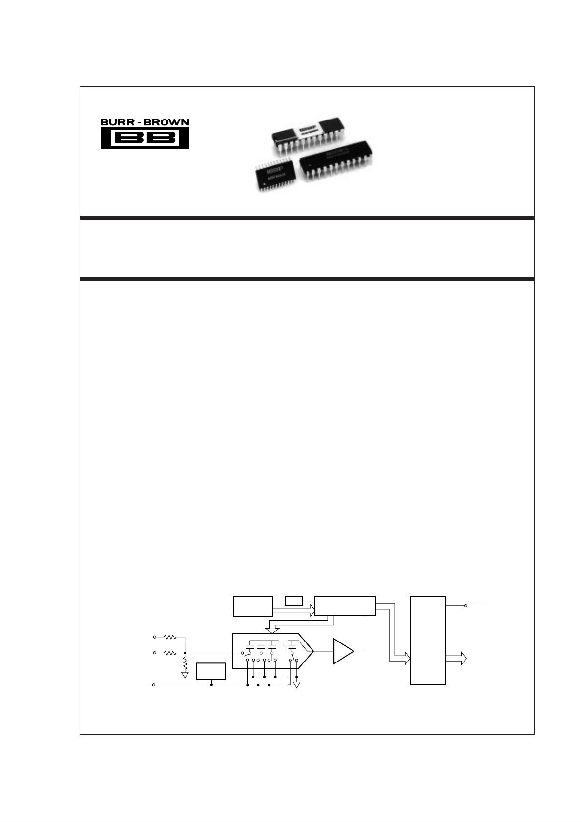
Comparator
Control
Logic
Internal
Ref
2V
Reference
Out
±5V
IN
±10V
IN
CDAC
SAR
BUSY
Three
State
Parallel
Output
Data
Bus
Clock
Output
Latches
And
Three
State
Drivers
®
ADS7800
DESCRIPTION
The ADS7800 is a complete 12-bit sampling analogto-digital converter using state-of-the-art CMOS structures. It contains a complete 12-bit successive approximation A/D converter with internal sample/hold,
reference, clock, digital interface for microprocessor
control, and three-state output drivers.
The ADS7800 is specified at a 333kHz sampling rate.
Conversion time is factory set for 2.70µs max over
temperature, and the high speed sampling input stage
insures a total acquisition and conversion time of 3µs
max over temperature. Precision, laser-trimmed scaling resistors provide industry-standard input ranges of
±5V or ±10V.
AC and DC performance are completely specified.
Two grades based on linearity and dynamic performance are available to provide the optimum price/
performance fit in a wide range of applications.
The 24-pin ADS7800 is available in plastic and sidebraze hermetic 0.3" wide DIPs, and in an SOIC
package. It operates from a +5V supply and either a
–12V or –15V supply. The ADS7800 is available in
grades specified over 0°C to +70°C and –40°C to
+85°C temperature ranges.
International Airport Industrial Park • Mailing Address: PO Box 11400, Tucson, AZ 85734 • Street Address: 6730 S. Tucson Blvd., Tucson, AZ 85706 • Tel: (520) 746-1111 • Twx: 910-952-1111
Internet: http://www.burr-brown.com/ • FAXLine: (800) 548-6133 (US/Canada Only) • Cable: BBRCORP • Telex: 066-6491 • FAX: (520) 889-1510 • Immediate Product Info: (800) 548-6132

®
ADS7800
2
SPECIFICATIONS
ELECTRICAL
At TA = T
MIN
to T
MAX
, Sampling Frequency, fS, = 333kHz, –VS = –15V, VS = +5V, unless otherwise specified.
ADS7800JP/JU/AH ADS7800KP/KU/BH
PARAMETER CONDITIONS MIN TYP MAX MIN TYP MAX UNITS
RESOLUTION 12 * Bits
ANALOG INPUT
Voltage Ranges ±10V/±5V * V
Impedance ±10V Range 4.4 6.3 8.1 * * * kΩ
±5V Range 2.9 4.2 5.4 * * * kΩ
THROUGHPUT SPEED
Conversion Time Conversion Alone 2.5 2.7 * * µs
Complete Cycle Acquisition + Conversion 2.6 3.0 * * µs
Throughput Rate 333 380 * * kHz
DC ACCURACY
Full Scale Error
(1)
±0.50 ±0.35 %
Full Scale Error Drift 6 * ppm/°C
Integral Linearity Error ±1 ±1/2 LSB
(2)
Differential Linearity Error ±1 ±3/4 LSB
No Missing Codes Guaranteed Guaranteed
Bipolar Zero
(1)
±4 ±2 LSB
Bipolar Zero Drift 1 * ppm/°C
Power Supply Sensitivity
–16.5V < –V
S
< –13.5V ±1/2 * LSB
–12.6V < –V
S
< –11.4V ±1/2 * LSB
+4.75V < V
S
< +5.25V ±1 ±1/2 LSB
Transition Noise
(3)
0.1 * LSB
AC ACCURACY
Spurious-Free Dynamic Range f
IN
= 47kHz 74 77 77 80 dB
(4)
Total Harmonic Distortion fIN = 47kHz –77 –74 –80 –77 dB
Two-tone Intermodulation Distortion f
IN1
= 24.4kHz (–6dB) –77 –74 –80 –77 dB
f
IN2
= 28.5kHz (–6dB)
Signal-to-(Noise + Distortion) Ratio f
IN
= 47kHz 67 70 69 72 dB
Signal-to-Noise Ratio (SNR) f
IN
= 47kHz 68 71 70 73 dB
SAMPLING DYNAMICS
Aperture Delay 13 * ns
Aperture Jitter 150 * ps, rms
Transient Response
(5)
130 * ns
Overvoltage Recovery
(6)
150 * ns
INTERNAL REFERENCE VOLTAGE
Voltage 1.9 2.0 2.1 * * * V
Source Current Available 10 * µA
for External Loads
DIGITAL INPUTS
Logic Levels
V
IL
–0.3 +0.8 * * V
V
IH
+2.4 +5.3 * * V
I
IL
–5 * µA
I
IH
+5 * µA
DIGITAL OUTPUTS
Data Format Parallel, 12-bit or 8-bit/4-bit
Data Coding Binary Offset Binary
V
OL
I
SINK
= 1.6mA 0.0 +0.4 * * V
V
OH
I
SOURCE
= 500µA +2.4 +5.0 * * V
I
LEAKAGE
(High-Z State) ±0.1 ±5**µA
POWER SUPPLIES
Rated Voltage
–V
S
–11.4 –15 –16.5 * * * V
V
S
(VSA and VSD) +4.75 +5.0 +5.25 * * * V
Current
–I
S
3.5 6 * * mA
I
S
18 25 * * mA
Power Consumption 135 215 * * mW

®
3
ADS7800
SPECIFICATIONS (CONT)
ELECTRICAL
At TA = T
MIN
to T
MAX
, Sampling Frequency, fS, = 333kHz, –VS = –15V, VS = +5V, unless otherwise specified.
ADS7800JP/JU/AH ADS7800KP/KU/BH
PARAMETER CONDITIONS MIN TYP MAX MIN TYP MAX UNITS
TEMPERATURE RANGE
Specification JP/JU/KP/KU 0 +70 * * °C
AH/BH –40 +85 * * °C
Operating JP/KP/JU/KU –40 +85 * * °C
Storage –65 +150 * * °C
* Same as specification for ADS7800JP/JU/AH.
NOTES: (1) Adjustable to zero with external potentiometer. (2) LSB means Least Significant Bit. For ADS7800, 1LSB = 2.44mV for the ±5V range, 1LSB =
4.88mV for the ±10V range. (3) Noise was characterized over temperature near full scale, 0V, and negative full scale. 0.1LSB represents a typical rms level of
noise at the worst case, which was near full scale input at +125°C. (4) All specifications in dB are referred to a full-scale input, either ±10V or ±5V. (5) For full
scale step input, 12-bit accuracy attained in specified time. (6) Recovers to specified performance in specified time after 2 x F
S
input overvoltage.
The information provided herein is believed to be reliable; however, BURR-BROWN assumes no responsibility for inaccuracies or omissions. BURR-BROWN assumes
no responsibility for the use of this information, and all use of such information shall be entirely at the user's own risk. Prices and specifications are subject to change
without notice. No patent rights or licenses to any of the circuits described herein are implied or granted to any third party. BURR-BROWN does not authorize or warrant
any BURR-BROWN product for use in life support devices and/or systems.
ABSOLUTE MAXIMUM RATINGS
–VS to ANALOG COMMON ............................................................ –16.5V
V
S
to DIGITAL COMMON .................................................................... +7V
Pin 23 (V
SD
) to Pin 24 (VSA)........................................................... ±0.3V
ANALOG COMMON to DIGITAL COMMON........................................±1V
Control Inputs to DIGITAL COMMON ............................. –0.3 to V
S
+ 0.3V
Analog Input Voltage.......................................................................... ±20V
Maximum Junction Temperature ..................................................... 160°C
Internal Power Dissipation ............................................................. 750mW
Lead Temperature (soldering, 10s)................................................ +300°C
Thermal Resistance,
θ
JA
:
Plastic DIP ................................................................................ 100°C/W
SOIC ......................................................................................... 100°C/W
Ceramic ...................................................................................... 50°C/W
ELECTROSTATIC
DISCHARGE SENSITIVITY
The ADS7800 is an ESD (electrostatic discharge) sensitive
device. The digital control inputs have a special FET structure, which turns on when the input exceeds the supply by
18V, to minimize ESD damage. However, permanent damage
may occur on unconnected devices subject to high energy
electrostatic fields. When not in use, devices must be stored in
conductive foam or shunts. The protective foam should be
discharged to the destination socket before devices are removed.
PACKAGE/ORDERING INFORMATION
INTEGRAL SIGNAL-TO- SPECIFICATION
LINEARITY (NOISE+DISTORTION) TEMPERATURE PACKAGE DRAWING
PRODUCT ERROR (LSB) RATIO (dB min) RANGE (
°C) PACKAGE NUMBER
(1)
ADS7800JP ±1 67 0 to +70 24-Pin Plastic DIP 243
ADS7800KP ±1/2 69 0 to +70 24-Pin Plastic DIP 243
ADS7800JU ±1 67 0 to +70 24-Pin Plastic SOIC 239
ADS7800KU ±1/2 69 0 to +70 24-Pin Plastic SOIC 239
ADS7800AH ±1 67 –40 to +85 24-Pin Ceramic DIP 245
ADS7800BH ±1/2 69 –40 to +85 24-Pin Ceramic DIP 245
NOTE: (1) For detailed drawing and dimension table, please see end of data sheet, or Appendix C of Burr-Brown IC Data Book.

®
ADS7800
4
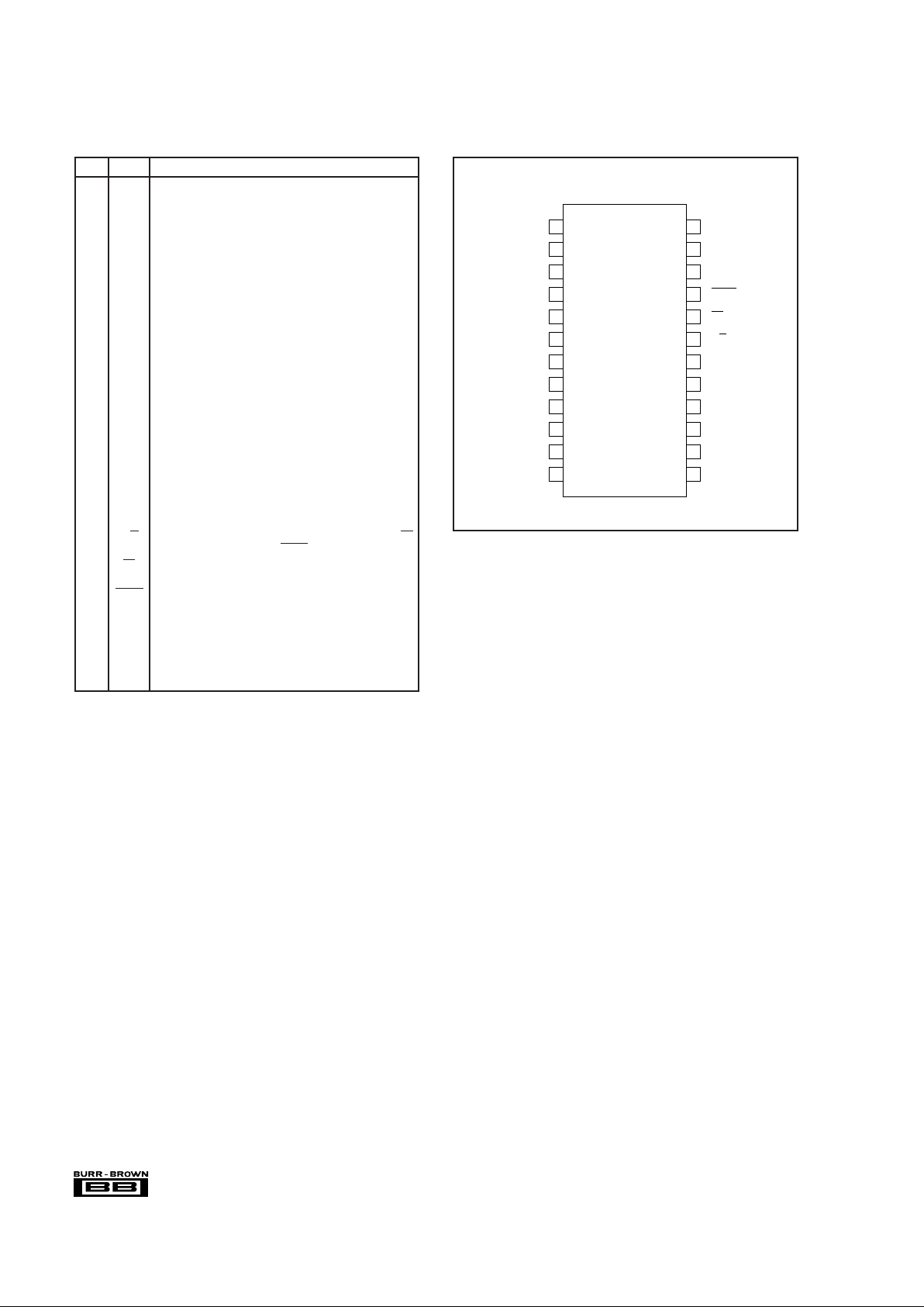
PIN ASSIGNMENTS
PIN # NAME DESCRIPTION
1 IN1 ±10V Analog Input. Connected to GND for ±5V range.
2 IN2 ±5V Analog Input. Connected to GND for ±10V range.
3 REF +2V Reference Output. Bypass to GND with 22µF to
47µF Tantalum. Buffer for external loads.
4 AGND Analog Ground. Connect to pin 13.
5 D11 Data Bit 11. Most Significant Bit (MSB).
6 D10 Data Bit 10.
7 D9 Data Bit 9.
8 D8 Data Bit 8.
9 D7 Data Bit 7 if HBE is LOW; LOW if HBE is HIGH.
10 D6 Data Bit 6 if HBE is LOW; LOW if HBE is HIGH.
11 D5 Data Bit 5 if HBE is LOW; LOW if HBE is HIGH.
12 D4 Data Bit 4 if HBE is LOW; LOW if HBE is HIGH.
13 DGND Digital Ground. Connect to pin 4.
14 D3 Data Bit 3 if HBE is LOW; Data Bit 11 if HBE is HIGH.
15 D2 Data Bit 2 if HBE is LOW; Data Bit 10 if HBE is HIGH.
16 D1 Data Bit 1 if HBE is LOW; Data Bit 9 if HBE is HIGH.
17 D0 Data Bit 0 if HBE is LOW. Least Significant Bit (LSB);
Data Bit 8 if HBE is HIGH.
18 HBE High Byte Enable. When held LOW, data output as 12-
bits in parallel. When held HIGH, four MSBs presented on
pins 14-17, pins 9-12 output LOWs. Must be LOW to
initiate conversion.
19 R/C Read/Convert. Falling edge initiates conversion when CS
is LOW, HBE is LOW, and BUSY is HIGH.
20 CS Chip Select. Outputs in Hi-Z state when HIGH. Must be
LOW to initiate conversion or read data.
21 BUSY Busy. Output LOW during conversion. Data valid on rising
edge in Convert Mode.
22 –V
S
Negative Power Supply. –12V or –15V. Bypass to GND.
23 V
SD
Positive Digital Power Supply. +5V. Connect to pin 24,
and bypass to GND.
24 V
SA
Positive Analog Power Supply. +5V. Connect to pin 23,
and bypass to GND.
PIN CONFIGURATION
Top View DIP/SOIC
1
2
3
4
5
6
7
8
9
10
11
12
IN1
IN2
REF
AGND
D11
D10
D9
D8
D7
D6
D5
D4
24
23
22
21
20
19
18
17
16
15
14
13
V
V
–V
BUSY
CS
R/C
HBE
D0
D1
D2
D3
DGND
SA
SD
S
 Loading...