Burr Brown Corporation ADS1286UB-2K5, ADS1286UB, ADS1286UA-2K5, ADS1286UA, ADS1286U-2K5 Datasheet
...
ADS1286
DESCRIPTION
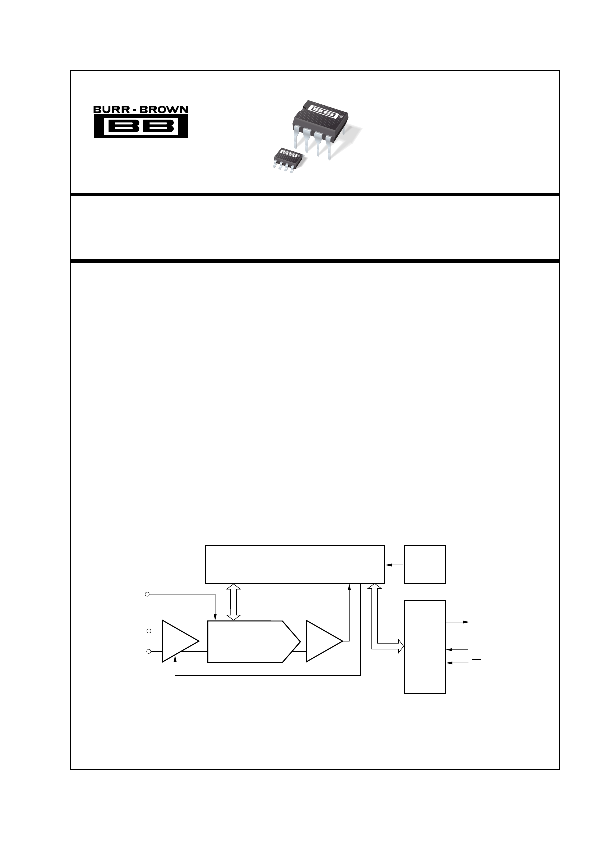
The ADS1286 is a 12-bit, 20kHz analog-to-digital
converter with a differential input and sample and hold
amplifier and consumes only 250µA of supply current. The ADS1286 offers an SPI and SSI compatible
serial interface for communications over a two or three
wire interface. The combination of a serial two wire
interface and micropower consumption makes the
ADS1286 ideal for remote applications and for those
requiring isolation.
The ADS1286 is available in a 8-pin plastic mini DIP
and a 8-lead SOIC.
12-Bit Micro Power Sampling
ANALOG-TO-DIGITAL CONVERTER
®
FEATURES
● SERIAL INTERFACE
● GUARANTEED NO MISSING CODES
● 20kHz SAMPLING RATE
● LOW SUPPLY CURRENT: 250µA
SAR
Control
Serial
Interface
D
OUT
Comparator
S/H Amp
CS/SHDN
DCLOCK
+In
V
REF
–In
CDAC
ADS1286
ADS1286
APPLICATIONS
● REMOTE DATA ACQUISITION
● ISOLATED DATA ACQUISITION
● TRANSDUCER INTERFACE
● BATTERY OPERATED SYSTEMS
©
1996 Burr-Brown Corporation PDS-1335B Printed in U.S.A. October, 1998
International Airport Industrial Park • Mailing Address: PO Box 11400, Tucson, AZ 85734 • Street Address: 6730 S. Tucson Blvd., Tucson, AZ 85706 • Tel: (520) 746-1111
Twx: 910-952-1111 • Internet: http://www.burr-brown.com/ • Cable: BBRCORP • Telex: 066-6491 • FAX: (520) 889-1510 • Immediate Product Info: (800) 548-6132

2
®
ADS1286
SPECIFICATIONS
At TA = T
MIN
to T
MAX
, +VCC = +5V, V
REF
= +5V, f
SAMPLE
= 12.5kHz, , f
CLK
= 16 • f
SAMPLE
, unless otherwise specified.
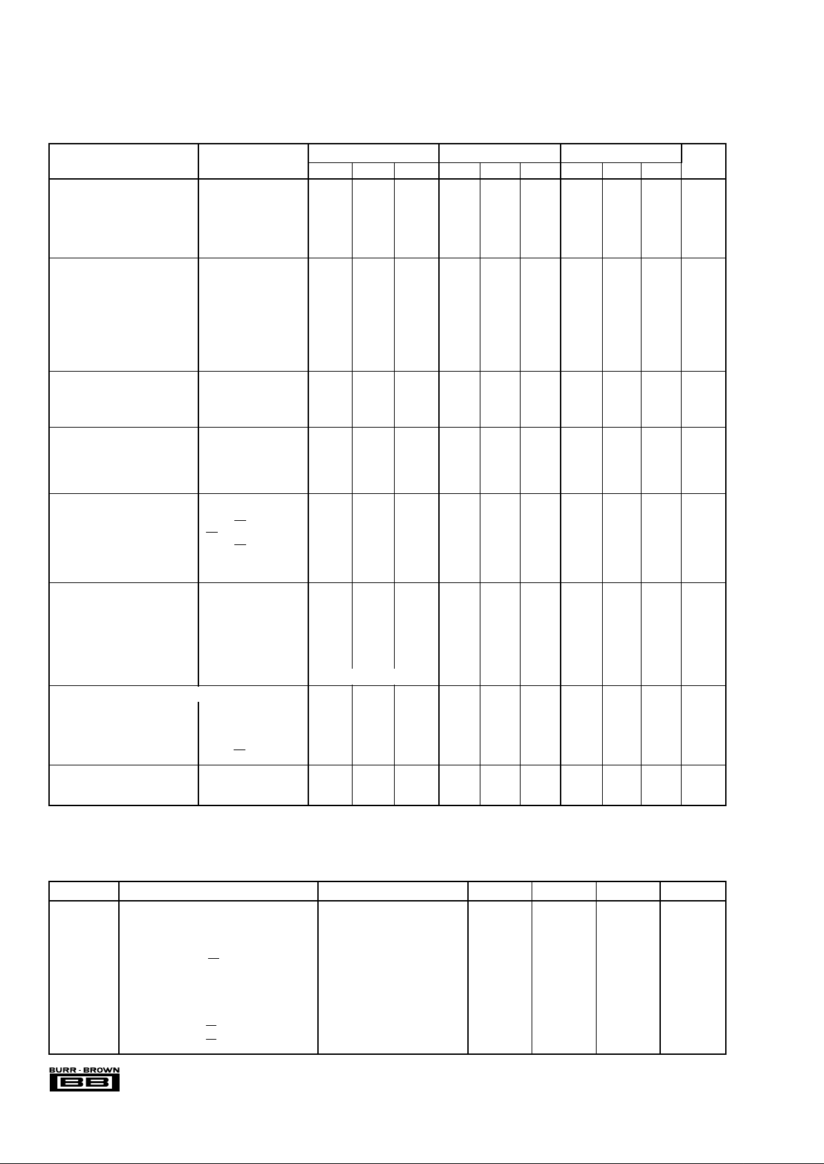
TIMING CHARACTERISTICS
f
CLK
= 200kHz, TA = T
MIN
to T
MAX
.
SYMBOL PARAMETER CONDITIONS MIN TYP MAX UNITS
t
SMPL
Analog Input Sample Time See Operating Sequence 1.5 2.0 Clk Cycles
t
SMPL (MAX)
Maximum Sampling Frequency ADS1286 20 kHz
t
CONV
Conversion Time See Operating Sequence 12 Clk Cycles
t
dDO
Delay TIme, DCLOCK↓ to D
OUT
Data Valid See Test Circuits 85 150 ns
t
dis
Delay TIme, CS↑ to D
OUT
Hi-Z See Test Circuits 25 50 ns
t
en
Delay TIme, DCLOCK↓ to D
OUT
Enable See Test Circuits 50 100 ns
t
hDO
Output Data Remains Valid After DCLOCK↓ C
LOAD
= 100pF 15 30 ns
t
f
D
OUT
Fall Time See Test Circuits 70 100 ns
t
r
D
OUT
Rise Time See Test Circuits 60 100 ns
t
CSD
Delay Time, CS↓ to DCLOCK↓ See Operating Sequence 0 ns
t
SUCS
Delay Time, CS↓ to DCLOCK↑ See Operating Sequence 30 ns
ADS1286, ADS1286A ADS1286K, ADS1286B ADS1286C, ADS1286L
PARAMETER CONDITIONS MIN TYP MAX MIN TYP MAX MIN TYP MAX UNITS
ANALOG INPUT
Full-Scale Input Range +In – (–In) 0 V
REF
✻✻✻✻V
Absolute Input Voltage +In –0.2 V
CC
+0.2 ✻✻✻✻V
–In –0.2 +0.2 ✻✻✻✻V
Capacitance 25 ✻✻pF
Leakage Current ±1 ✻✻µA
SYSTEM PERFORMANCE
Resolution 12 ✻✻Bits
No Missing Codes 12 ✻✻Bits
Integral Linearity ±1 ±2 ✻✻ ±0.5 ±1 LSB
Differential Linearity ±0.5 ±1.0 ✻ ±0.75 ±0.25 ±0.75 LSB
Offset Error 0.75 ±3 ✻✻ ✻✻LSB
Gain Error ±2 ±8 ✻✻ ✻✻LSB
Noise 50 ✻✻µVrms
Power Supply Rejection 82 ✻✻dB
SAMPLING DYNAMICS
Conversion Time 12 ✻✻
Clk Cycles
Acquisition Time 1.5 ✻✻
Clk Cycles
Small Signal Bandwidth 500 ✻✻kHz
DYNAMIC CHARACTERISTICS
Total Harmonic Distortion V
IN
= 5.0Vp-p at 1kHz –85 ✻✻dB
V
IN
= 5.0Vp-p at 5kHz –83 ✻✻dB
SINAD V
IN
= 5.0Vp-p at 1kHz 72 ✻✻dB
Spurious Free Dynamic Range V
IN
= 5.0Vp-p at 1kHz 90 ✻✻dB
REFERENCE INPUT
REF Input Range 1.25 2.5
VCC+0.05V
✻✻✻✻✻✻V
Input Resistance CS = V
CC
5000 ✻✻MΩ
CS = GND, f
CLK
= 0Hz 5000 ✻✻MΩ
Current Drain CS = V
CC
0.01
2.5
✻✻ ✻✻µA
t
CYC
≥ 640µs, f
CLK
≤ 25kHz
2.4
20
✻✻ ✻✻µA
t
CYC
= 80µs, f
CLK
= 200kHz
2.4
20
✻✻ ✻✻µA
DIGITAL INPUT/OUTPUT
Logic Family CMOS ✻✻
Logic Levels:
V
IH
IIH = +5µA3 +VCC✻✻✻✻V
V
IL
IIL = +5µA 0.0 0.8 ✻✻✻✻V
V
OH
IOH = 250µA3 +VCC✻✻✻✻V
V
OL
IOL = 250µA 0.0 0.4 ✻✻✻✻V
Data Format Straight Binary ✻✻
POWER SUPPLY REQUIREMENTS
Power Supply Voltage
V
CC
+4.50 5 5.25 ✻✻✻✻✻✻V
Quiescent Current, V
ANA
t
CYC
≥ 640µS, f
CLK
≤ 25kHz
200 400 ✻✻ ✻✻µA
t
CYC
= 90µS, f
CLK
= 200kHz
250 500 ✻✻ ✻✻µA
Power Down CS = V
CC
3 ✻✻µA
TEMPERATURE RANGE
Specified Performance ADS1286, K, L 0 +70 ✻✻✻✻°C
ADS1286A, B, C –40 +85 ✻✻✻✻°C
✻ Specifications same as grade to the left.

3
®
ADS1286
ELECTROSTATIC
DISCHARGE SENSITIVITY
Electrostatic discharge can cause damage ranging from performance degradation to complete device failure. BurrBrown Corporation recommends that all integrated circuits
be handled and stored using appropriate ESD protection
methods.
ESD damage can range from subtle performance degradation to complete device failure. Precision integrated circuits
may be more susceptible to damage because very small
parametric changes could cause the device not to meet
published specifications.
ABSOLUTE MAXIMUM RATINGS
(1)
+VCC.....................................................................................................+6V
Analog Input....................................................... –0.3V to (+V
CC
+ 300mV)
Logic Input .........................................................–0.3V to (+V
CC
+ 300mV)
Case Temperature ......................................................................... +100°C
Junction Temperature .................................................................... +150°C
Storage Temperature..................................................................... +125°C
External Reference Voltage .............................................................. +5.5V
NOTE: (1) Stresses above these ratings may permanently damage the device.
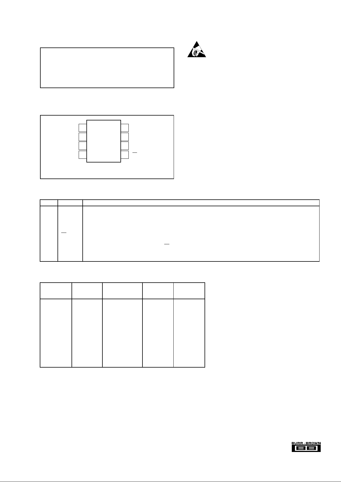
PIN CONFIGURATION
1
2
3
4
8
7
6
5
+V
CC
DCLOCK
D
OUT
CS/SHDN
V
REF
+In
–In
GND
ADS1286
8-Pin Mini PDIP
8-Lead SOIC
PIN ASSIGNMENTS
PIN NAME DESCRIPTION
1V
REF
Reference Input.
2 +In Non Inverting Input.
3 –In Inverting Input. Connect to ground or remote ground sense point.
4 GND Ground.
5 CS/SHDN Chip Select when low, Shutdown Mode when high.
6D
OUT
The serial output data word is comprised of 12 bits of data. In operation the data is valid on the falling edge of DCLOCK. The
second clock pulse after the falling edge of CS enables the serial output. After one null bit the data is valid for the next 12 edges.
7 DCLOCK Data Clock synchronizes the serial data transfer and determines conversion speed.
8+V
CC
Power Supply.
PACKAGE
INTEGRAL TEMPERATURE DRAWING
PRODUCT LINEARITY RANGE PACKAGE NUMBER
(1)
ADS1286P ±20°C to +70°C Plastic DIP 006
ADS1286PK ±20°C to +70°C Plastic DIP 006
ADS1286PL ±10°C to +70°C Plastic DIP 006
ADS1286U ±20°C to +70°C SOIC 182
ADS1286UK ±20°C to +70°C SOIC 182
ADS1286UL ±10°C to +70°C SOIC 182
ADS1286PA ±2 –40°C to +85°C Plastic DIP 006
ADS1286PB ±2 –40°C to +85°C Plastic DIP 006
ADS1286PC ±1 –40°C to +85°C Plastic DIP 006
ADS1286UA ±2 –40°C to +85°C SOIC 182
ADS1286UB ±2 –40°C to +85°C SOIC 182
ADS1286UC ±1 –40°C to +85°C SOIC 182
PACKAGE/ORDERING INFORMATION
NOTE: (1) For detailed drawing and dimension table, please see end of data sheet, or Appendix
C of Burr-Brown IC Data Book.
The information provided herein is believed to be reliable; however, BURR-BROWN assumes no responsibility for inaccuracies or omissions. BURR-BROWN
assumes no responsibility for the use of this information, and all use of such information shall be entirely at the user’s own risk. Prices and specifications are subject
to change without notice. No patent rights or licenses to any of the circuits described herein are implied or granted to any third party. BURR-BROWN does not
authorize or warrant any BURR-BROWN product for use in life support devices and/or systems.

4
®
ADS1286
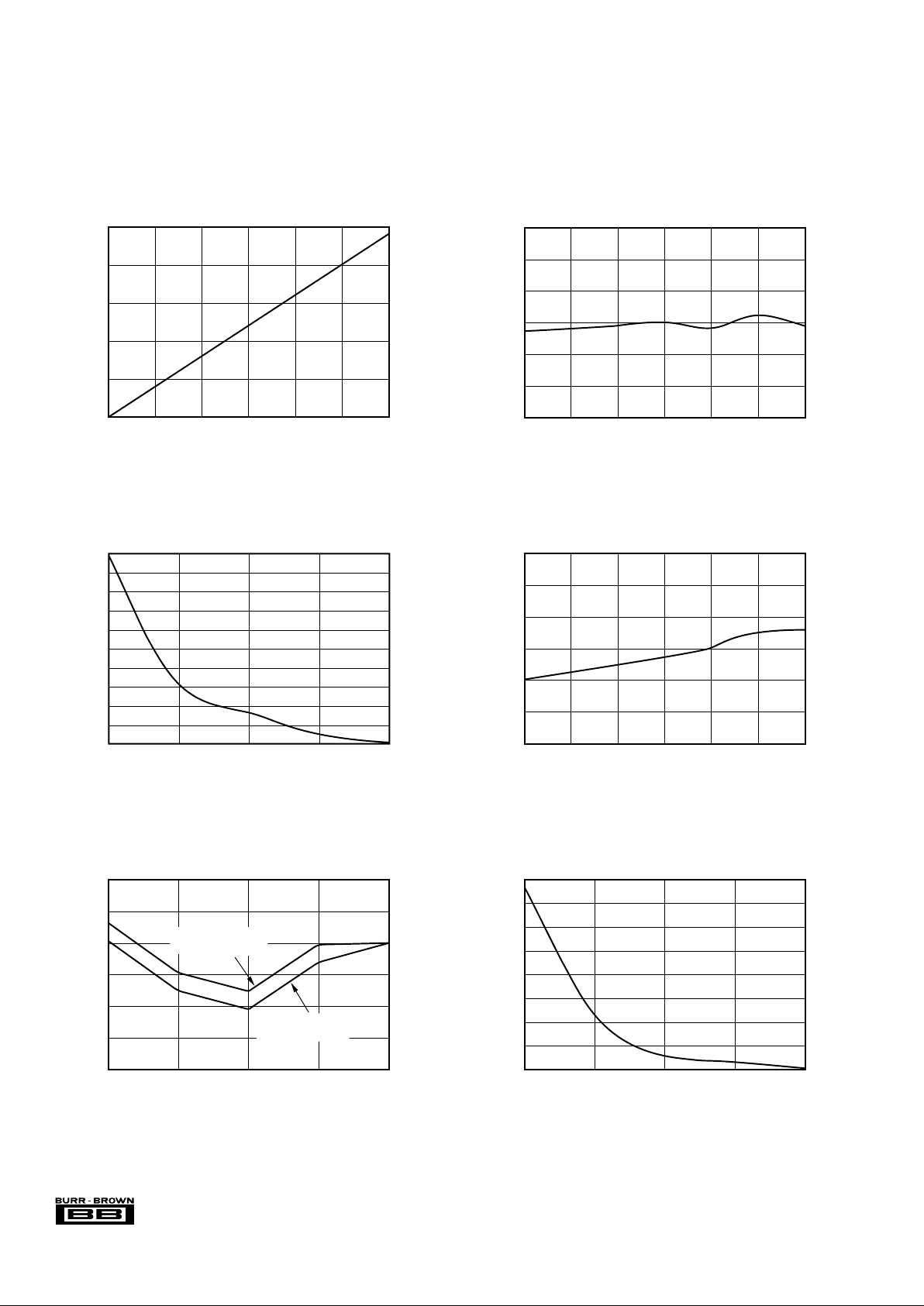
TYPICAL PERFORMANCE CURVES
At TA = +25, VCC = +5V, V
REF
= +5V, f
SAMPLE
= 12.5kHz, f
CLK
= 16 • f
SAMPLE
, unless otherwise specified.
REFERENCE CURRENT vs TEMPERATURE
4.0
3.5
3.0
2.5
2.0
1.5
1.0
Reference Current (µA)
–55 –40 –25 0 25 70 85
Temperature (°C)
CHANGE IN OFFSET vs REFERENCE VOLTAGE
5
4.5
4
3.5
3
2.5
2
1.5
1
0.5
0
Change in Offset (LSB)
12345
Reference Voltage (V)
CHANGE IN OFFSET vs TEMPERATURE
0.6
0.4
0.2
0
–0.2
–0.4
–0.6
Delta from 25°C (LSB)
–55 –40 –25 0 25 70 85
Temperature (°C)
CHANGE IN INTEGRAL LINEARITY AND DIFFERENTIAL
LINEARITY vs REFERENCE VOLTAGE
0.10
0.05
0.00
–0.05
–0.10
–0.15
–0.20
Delta from +5V Reference (LSB)
12345
Reference Voltage (V)
Change in Differential
Linearity (LSB)
Change in Integral
Linearity (LSB)
CHANGE IN GAIN vs REFERENCE VOLTAGE
4
3.5
3
2.5
2
1.5
1
0.5
0
Change in Gain (LSB)
12345
Reference Voltage (V)
REFERENCE CURRENT vs SAMPLE RATE
2.5
2.0
1.5
1.0
0.5
0
Reference Current (µA)
024681012
Sample Rate (kHz)
 Loading...