

Burr Brown Corporation ADS1250U, ADS1250U-1K Datasheet
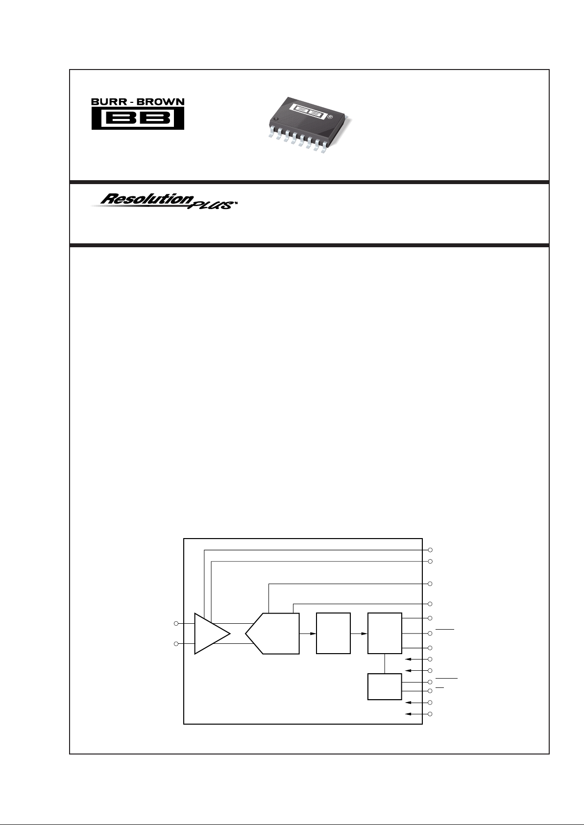
20-Bit Data Acquisition System
ANALOG-TO-DIGITAL CONVERTER
ADS1250
®
FEATURES
● 20 BITS NO MISSING CODES
● 18 BITS EFFECTIVE RESOLUTION UP TO
25kHz DATA RATE
● LOW NOISE: 2.8ppm at PGA = 1
● DIFFERENTIAL INPUTS
● INL: 0.002% (MAX)
● PROGRAMMABLE FULL SCALE
● I/O CONTROLLED PGA: 1, 2, 4, 8
● EXTERNAL REFERENCE
DESCRIPTION
The ADS1250 is a precision, wide dynamic range,
delta-sigma, analog-to-digital converter with 20-bit
resolution operating from a single +5V supply. The
delta-sigma architecture is used for wide dynamic
range and to guarantee 20 bits of no missing code
performance. An effective resolution of 18 bits (2.8ppm
of rms noise) is achieved for conversion rates up to
25kHz. The dynamic range of the converter is further
increased by providing a low-noise Programmable
Gain Amplifier (PGA) with gain stages of 1, 2, 4, or
8 for low level input signals.
The ADS1250 is designed for high-resolution measurement applications in cardiac diagnostics, smart
transmitters, industrial process control, weigh scales,
chromatography and portable instrumentation. The
converter includes a flexible synchronous serial interface and offers a three-wire control mode for low-cost
isolation.
The ADS1250 is a single-channel converter and is
offered in an SOL-16 package.
APPLICATIONS
● CARDIAC DIAGNOSTICS
● DIRECT THERMOCOUPLE INTERFACE
● BLOOD ANALYSIS
● INFRARED PYROMETER
● LIQUID/GAS CHROMATOGRAPHY
● PRECISION PROCESS CONTROL
©
1999 Burr-Brown Corporation PDS-1520B Printed in U.S.A. December, 1999
International Airport Industrial Park • Mailing Address: PO Box 11400, Tucson, AZ 85734 • Street Address: 6730 S. Tucson Blvd., Tucson, AZ 85706 • Tel: (520) 746-1111
Twx: 910-952-1111 • Internet: http://www.burr-brown.com/ • Cable: BBRCORP • Telex: 066-6491 • FAX: (520) 889-1510 • Immediate Product Info: (800) 548-6132
4th-Order
∆Σ
Modulator
Digital
Filter
Serial
Output
Control
PGA
+V
IN
G0
G1
CLK
V
REF
SCLK
DRDY
DOUT
+V
S
AGND
DSYNC
CS
+V
D
DGND
–V
IN
+
–
ADS1250
ADS1250
For most current data sheet and other product
information, visit www.burr-brown.com

2
ADS1250
®
SPECIFICATIONS
All specifications at T
MIN
to T
MAX
, VD = VS = +5V, CLK = 9.6MHz, PGA = 1, and V
REF
= 4.096, unless otherwise specified.
ADS1250U
PARAMETER CONDITIONS MIN TYP MAX UNITS
ANALOG INPUT
Input Voltage Range
(1)
G = Gain AGND ±V
REF
/G V
Programmable Gain Amplifier 1 8
Input Impedance (differential) G = Gain 104/G kΩ
Input Capacitance G = Gain 6 • G pF
Input Leakage At +25°C550pA
At T
MIN
to T
MAX
1nA
DYNAMIC CHARACTERISTICS
Data Rate 25 kHz
Bandwidth 3dB 5.4 kHz
Serial Clock (SCLK) 9.6 MHz
System Clock Input (CLK) 9.6 MHz
ACCURACY
Integral Linearity Error
(2)
±0.0012 ±0.0020 % of FSR
THD 1kHz Input; 0.1dB below FS 97 dB
Noise 2.8 3.8 ppm of FSR, rms
Resolution 20 Bits
No Missing Codes 20 Bits
Common-Mode Rejection
(3)
at DC 90 105 dB
Gain Error 1 % of FSR
Offset Error ±100 ±200 ppm of FSR
Gain Sensitivity to V
REF
V
REF
= 4.096V ±0.1V 1:1
Power Supply Rejection Ratio 60 78 dB
PERFORMANCE OVER TEMPERATURE
Offset Drift 0.25 ppm/°C
Gain Drift 5.0 ppm/°C
VOLTAGE REFERENCE
V
REF
3.996V 4.096 4.196 V
Load Current 125 µA
DIGITAL INPUT/OUTPUT
Logic Family CMOS
Logic Level: V
IH
+4.0 +VD + 0.3 V
V
IL
–0.3 +0.8 V
V
OH
IOH = –500µA +4.5 V
V
OL
IOL = 500µA 0.4 V
Data Format Binary Two’s Complement
POWER SUPPLY REQUIREMENTS
Operation +4.75 +5 +5.25 VDC
Quiescent Current, Analog V = +5VDC 14 mA
Quiescent Current, Digital V = +5VDC 1 mA
Operating Power 75 100 mW
TEMPERATURE RANGE
Operating –40 +85 °C
Storage –60 +100 °C
NOTES: (1) In order to achieve the converter’s full-scale range, the input must be fully differential. If the input is single-ended (+V
IN
or –VIN is fixed), then the
full-scale range is one-half that of the differential range. (2) Applies to full-differential signals. (3) The common-mode rejection test is performed with a 100mV
differential input.
3
®
ADS1250
PACKAGE SPECIFIED
DRAWING TEMPERATURE PACKAGE ORDERING TRANSPORT
PRODUCT PACKAGE NUMBER RANGE MARKING NUMBER
(1)
MEDIA
ADS1250U SOL-16 211 –40°C to +85°C ADS1250U ADS1250U Rails
" " " " " ADS1250U/1K Tape and Reel
NOTE: (1) Models with a slash (/) are available only in Tape and Reel in the quantities indicated (e.g., /1K indicates 1000 devices per reel). Ordering 1000 pieces
of “ADS1250U/1K” will get a single 1000-piece Tape and Reel.
PACKAGE/ORDERING INFORMATION
ELECTROSTATIC
DISCHARGE SENSITIVITY
This integrated circuit can be damaged by ESD. Burr-Brown
recommends that all integrated circuits be handled with appropriate precautions. Failure to observe proper handling and
installation procedures can cause damage.
Electrostatic discharge can cause damage ranging from
performance degradation to complete device failure. BurrBrown Corporation recommends that all integrated circuits be
handled and stored using appropriate ESD protection
methods.
Analog Input: Current................................................ ±100mA, Momentary
±10mA, Continuous
Voltage ....................................... AGND –0.3V to V
S
+ 0.3V
V
S
to VD....................................................................................–0.3V to 6V
V
S
to AGND ............................................................................ –0.3V to 6V
V
D
to DGND ............................................................................ –0.3V to 6V
AGND to DGND ................................................................................±0.3V
V
REF
Voltage to AGND ................................................. –0.3V to VS + 0.3V
Digital Input Voltage to DGND ..................................... –0.3V to V
D
+ 0.3V
Digital Output Voltage to DGND .................................. –0.3V to V
D
+ 0.3V
Lead Temperature (soldering, 10s) .............................................. +300°C
Power Dissipation (any package) .................................................. 500mW
ABSOLUTE MAXIMUM RATINGS
The information provided herein is believed to be reliable; however, BURR-BROWN assumes no responsibility for inaccuracies or omissions. BURR-BROWN assumes
no responsibility for the use of this information, and all use of such information shall be entirely at the user’s own risk. Prices and specifications are subject to change
without notice. No patent rights or licenses to any of the circuits described herein are implied or granted to any third party. BURR-BROWN does not authorize or warrant
any BURR-BROWN product for use in life support devices and/or systems.
4
ADS1250
®
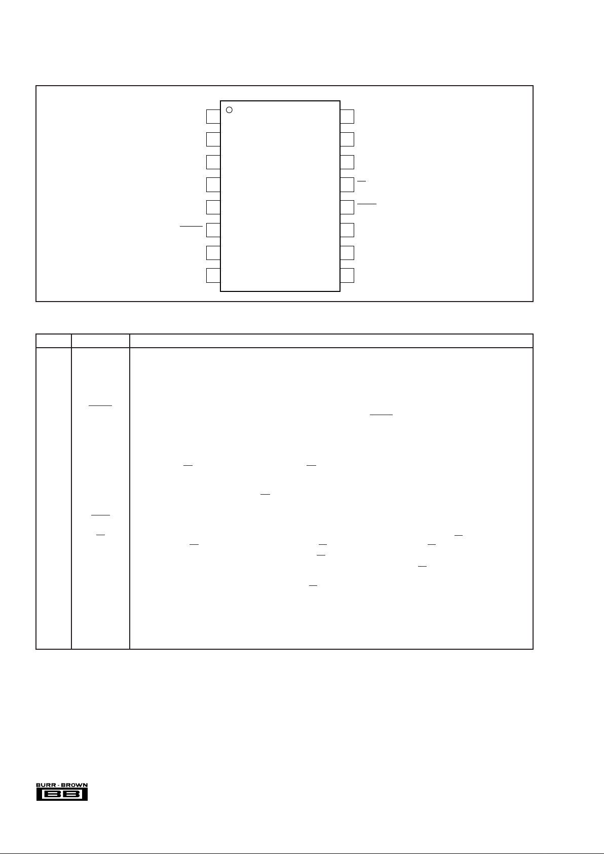
PIN DESCRIPTIONS
PIN NAME PIN DESCRIPTION
1+V
IN
Analog Input: Positive Input of the Differential Analog Input.
2–V
IN
Analog Input: Negative Input of the Differential Analog Input.
3 AGND Analog Input: Analog Ground.
4+V
S
Analog Input: Analog Power Supply Voltage, +5V.
5V
REF
Analog Input: Reference Voltage Input.
6 DSYNC Digital Input: Data Synchronization. A falling edge on this input will reset the modulator count and place the modulator in a hold
state. The modulator is released from the hold state on the rising edge of DSYNC. This can be used to synchronize multiple
ADS1250s.
7+V
D
Digital Input: Digital Power Supply Voltage, +5V.
8 DGND Digital Input: Digital Ground.
9 DOUT Digital Output: Serial Data Output. The serial data is clocked out of the serial data output shift register through this pin. The pin
is driven when CS is LOW, and high impedance when CS is HIGH.
10 SCLK Digital Input: Serial Clock. The serial clock is in the form of a CMOS-compatible clock. The serial clock can operate up to the
device’s system clock frequency. The serial clock can be either a free-running clock or noncontinuous clock, with either type of
clock; the serial data output is gated by CS.
11 CLK Digital Input: Device System Clock. The system clock is in the form of a CMOS-compatible clock.
12 DRDY Digital Output: Data Ready. A falling edge on this output indicates that a new output word is available from the ADS1250 data output
register.
13 CS Digital Input: Chip Select. Active LOW logic input used to enable serial data output from the ADS1250. CS controls the state of
the DOUT pin. If CS is HIGH, DOUT is high impedance; if CS is LOW, DOUT drives the bus. CS can be used in three ways:
(1)If the ADS1250 shares the bus with other devices, CS is used as serial data output enable for communications.
(2)If the ADS1250 shares the bus with other devices and SCLK is a free-running clock, CS is used to gate serial data
out of the device.
(3) If the ADS1250 is the only device on the bus, CS can be tied LOW to always enable serial data output for a
two-wire interface.
Refer to the Serial Communications section of this data sheet for more detail.
14 G0 Digital Input: Gain Selection Control (LSB).
15 G1 Digital Input: Gain Selection Control (MSB).
16 DGND Digital Input: Digital Ground.
PIN CONFIGURATION
1
2
3
4
5
6
7
8
16
15
14
13
12
11
10
9
+V
IN
ADS1250
AGND
–V
IN
+V
S
V
REF
DSYNC
+V
D
DGND
DGND
G0 (LSB)
G1 (MSB)
CS
DRDY
CLK
SCLK
DOUT
Top View SOL-16
5
®
ADS1250
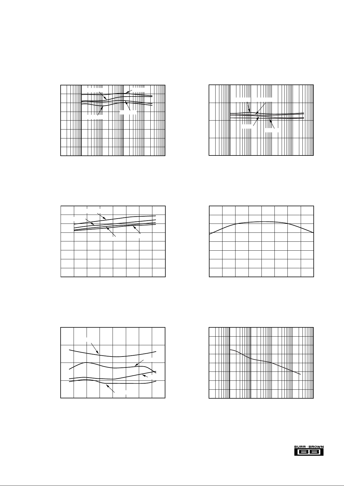
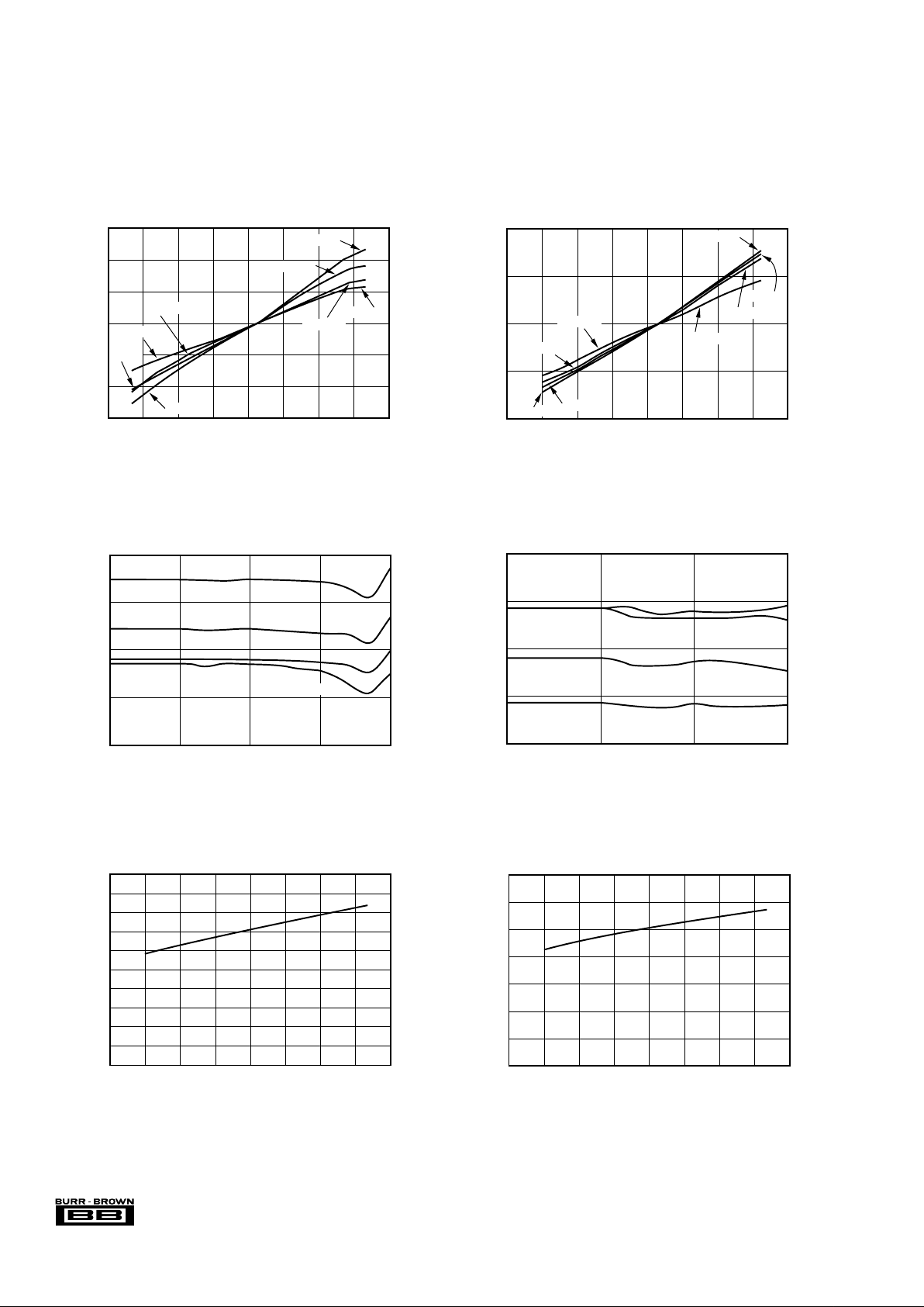
TYPICAL PERFORMANCE CURVES
At TA = +25°C, VD = VS = +5V, CLK = 9.6MHz, PGA = 1, and V
REF
= 4.096, unless otherwise specified.
4.0
3.5
3.0
2.5
2.0
1.5
1.0
0.5
0.0
RMS NOISE vs INPUT VOLTAGE (PGA = 1)
Differential Analog Input Voltage (V)
–4.0 –3.0 –2.0 –1.0 0.0 1.0 2.0 3.0 4.0
RMS Noise (ppm of FS)
20
15
10
5
0
INTEGRAL NON-LINEARITY vs TEMPERATURE
Temperature (°C)
–60 –40 –20 0 20 40 60 80 100
INL (ppm of FS)
PGA = 8
PGA = 2
PGA = 4
PGA = 1
4.0
3.5
3.0
2.5
2.0
1.5
1.0
0.5
0.0
RMS NOISE vs TEMPERATURE
Temperature (°C)
–60 –40 –20 0 20 40 60 80 100
RMS Noise (ppm of FS)
PGA = 1
PGA = 8
PGA = 2
PGA = 4
RMS NOISE vs DATA OUTPUT RATE
4.0
3.5
3.0
2.5
2.0
1.5
1.0
0.5
0.0
10 100 1000 10000 100001
Data Output Rate (Hz)
RMS Noise (ppm of FS)
PGA = 1
PGA = 8
PGA = 2
PGA = 4
EFFECTIVE RESOLUTION
vs DATA OUTPUT RATE
20.0
19.0
18.0
17.0
16.0
10 100 1000 10000 100001
Data Output Rate (Hz)
Effective Resolution Bits (rms)
PGA = 1
PGA = 8
PGA = 2
PGA = 4
INTEGRAL NON-LINEARITY
vs DATA OUTPUT RATE (PGA = 1)
14.0
13.5
13.0
12.5
12.0
11.5
11.0
10.5
10.0
10 100 1000 10000 100001
Data Output Rate (Hz)
INL (ppm of FS)
6
ADS1250
®
TYPICAL PERFORMANCE CURVES (Cont.)
At TA = +25°C, VD = VS = +5V, CLK = 9.6MHz, PGA = 1, and V
REF
= 4.096, unless otherwise specified.
30
20
10
0
–10
–20
–30
OFFSET DRIFT vs TEMPERATURE
Temperature (°C)
–60 –40 0–20 4020 60 10080
Offset Drift (ppm of FS)
PGA = 2
PGA = 2
PGA = 4
PGA = 1
PGA = 4
PGA = 8
PGA = 8
PGA = 1
400
200
0
–200
–400
GAIN DRIFT vs TEMPERATURE
Temperature (°C)
–60 –40 0–20 4020 60 10080
Gain Drift (ppm of FS)
PGA = 2
PGA = 4
PGA = 1
PGA = 8
PGA = 2
PGA = 4
PGA = 8
PGA = 1
20.0
18.0
16.0
14.0
12.0
10.0
8.0
6.0
4.0
2.0
0.0
ANALOG CURRENT vs TEMPERATURE
(PGA = 1)
Temperature (°C)
–60 –40 0–20 4020 60 10080
Analog Current (mA)
1.4
1.2
1.0
0.8
0.6
0.4
0.2
0.0
DIGITAL CURRENT vs TEMPERATURE
(PGA = 1)
Temperature (°C)
–60 –40 0–20 4020 60 10080
Digital Current (mA)
100
90
80
70
60
POWER SUPPLY REJECTION RATIO
vs FREQUENCY
PGA = 8
Frequency (Hz)
1 10 100 1k 10k
PSRR (dB)
PGA = 4
PGA = 2
PGA = 1
COMMON-MODE REJECTION RATIO
vs FREQUENCY
120
115
110
105
100
PGA = 1
Frequency (Hz)
1 10 100 1000
CMRR (dB)
PGA = 2
PGA = 4
PGA = 8
 Loading...