Burr Brown Corporation ADS1213E, ADS1212U-1K, ADS1212U, ADS1212P, ADS1213U-1K Datasheet
...
ADS1213
ADS1213
ADS1212
ADS1213
ADS1212
ADS1212
ADS1213
PATENTS PENDING
®
22-Bit ANALOG-TO-DIGITAL CONVERTER
FEATURES
● DELTA-SIGMA A/D CONVERTER
● 22 BITS NO MISSING CODES
● 20 BITS EFFECTIVE RESOLUTION AT 10Hz
AND 16 BITS AT 1000Hz
● LOW POWER: 1.4mW
● DIFFERENTIAL INPUTS
● PROGRAMMABLE GAIN AMPLIFIER
● SPI COMPATIBLE SSI INTERFACE
● PROGRAMMABLE CUT-OFF FREQUENCY
UP TO 6.25kHz
● INTERNAL/EXTERNAL REFERENCE
● ON CHIP SELF-CALIBRATION
● ADS1213 INCLUDES 4 CHANNEL MUX
APPLICATIONS
● INDUSTRIAL PROCESS CONTROL
● INSTRUMENTATION
● BLOOD ANALYSIS
● SMART TRANSMITTERS
● PORTABLE INSTRUMENTS
● WEIGH SCALES
● PRESSURE TRANSDUCERS
AGND AVDDREF
OUT
DESCRIPTION
The ADS1212 and ADS1213 are precision, wide
dynamic range, delta-sigma analog-to-digital converters
with 24-bit resolution operating from a single +5V
supply. The differential inputs are ideal for direct
connection to transducers or low level voltage signals. The delta-sigma architecture is used for wide
dynamic range and to guarantee 22 bits of no missing
code performance. An effective resolution of 20 bits
is achieved through the use of a very low-noise input
amplifier at conversion rates up to 10Hz. Effective
resolutions of 16 bits can be maintained up to a
sample rate of 1kHz through the use of the unique
Turbo modulator mode of operation. The dynamic
range of the converters is further increased by providing a low-noise programmable gain amplifier with a
gain range of 1 to 16 in binary steps.
The ADS1212 and ADS1213 are designed for high
resolution measurement applications in smart transmitters, industrial process control, weigh scales, chromatography and portable instrumentation. Both converters include a flexible synchronous serial interface
which is SPI compatible and also offers a two-wire
control mode for low cost isolation.
The ADS1212 is a single channel converter and is
offered in both 18-pin DIP and 18-lead SOIC packages. The ADS1213 includes a 4 channel input multiplexer and is available in 24-pin DIP, 24-lead SOIC,
and 28-lead SSOP packages.
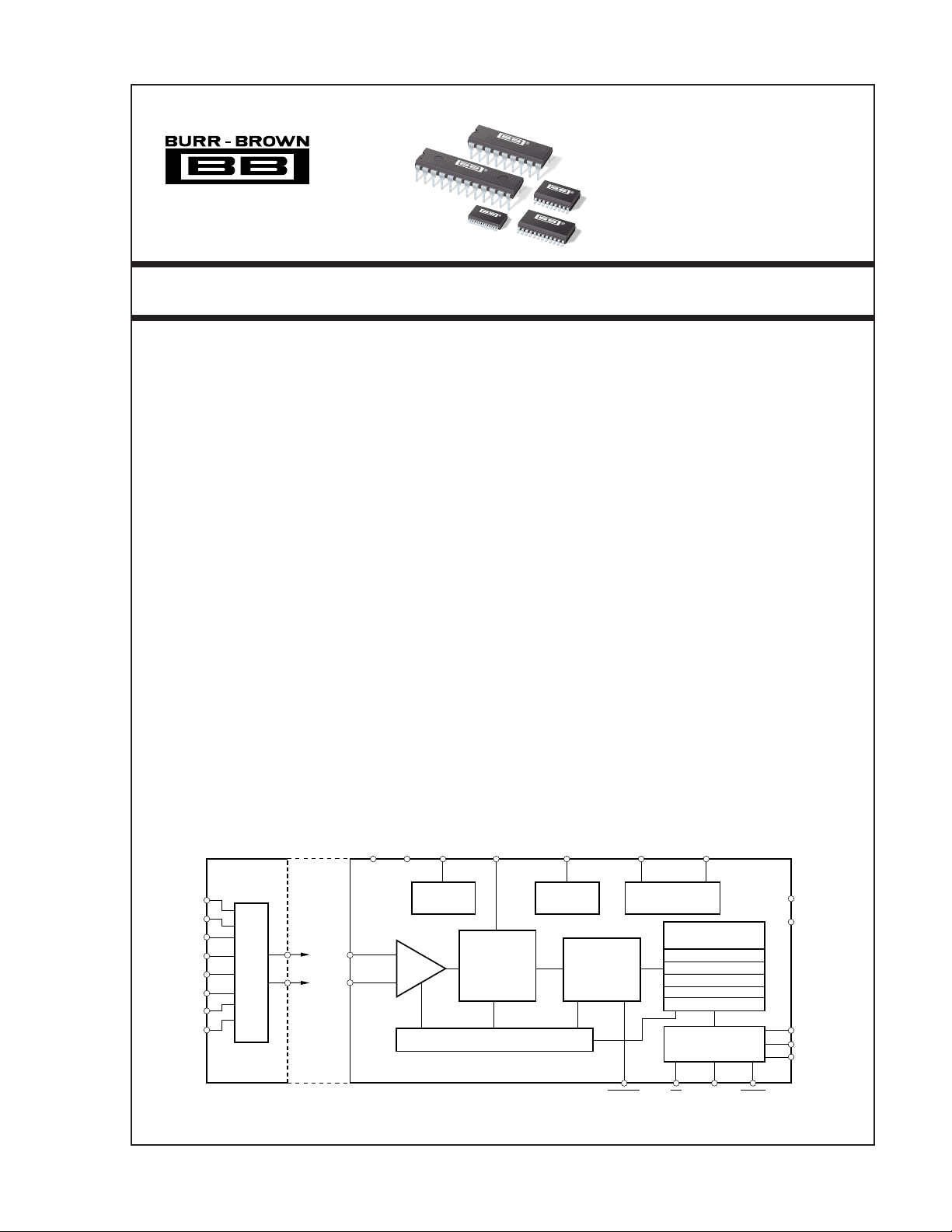
REF
IN
V
BIAS
X
IN
X
OUT
PGA
+2.5V
Reference
Second-Order
∆∑
Modulator
Modulator Control
A
1P
IN
1N
A
IN
2P
A
IN
2N
A
IN
AIN3P
3N
A
IN
4P
A
IN
4N
A
IN
International Airport Industrial Park • Mailing Address: PO Box 11400, Tucson, AZ 85734 • Street Address: 6730 S. Tucson Blvd., Tucson, AZ 85706 • Tel: (520) 746-1111 • Twx: 910-952-1111
Internet: http://www.burr-brown.com/ • FAXLine: (800) 548-6133 (US/Canada Only) • Cable: BBRCORP • Telex: 066-6491 • FAX: (520) 889-1510 • Immediate Product Info: (800) 548-6132
©
1996 Burr-Brown Corporation PDS-1360C Printed in U.S.A. April, 1998
MUX
ADS1213 Only ADS1212/13
AINP
A
IN
N
+3.3V Bias
Generator
Third-Order
Digital Filter
Clock Generator
Micro Controller
Instruction Register
Command Register
Data Output Register
Offset Register
Full-Scale Register
Serial Interface
DSYNC CS DRDY
MODE
1 ADS1212, 1213
DGND
DV
DD
SCLK
SDIO
SDOUT
®

SPECIFICATIONS
All specifications T
and external 2.5V reference, unless otherwise specified.
PARAMETER CONDITIONS MIN TYP MAX UNITS
ANALOG INPUT
Input Voltage Range
Input Impedance G = Gain, TMR = Turbo Mode Rate 20/(G • TMR)
Programmable Gain Amplifier User Programmable: 1, 2, 4, 8, or 16 1 16
Input Capacitance 5pF
Input Leakage Current At +25°C550pA
SYSTEMS PERFORMANCE
No Missing Codes f
Integral Linearity f
Unipolar Offset Error
Unipolar Offset Drift
Gain Error
Gain Error Drift
Common-Mode Rejection
Normal-Mode Rejection 50Hz, f
Output Noise See Typical Performance Curves
Power Supply Rejection DC, 50Hz, and 60Hz 60 dB
VOLTAGE REFERENCE
Internal Reference (REF
Drift 25 ppm/°C
Noise 50 µVp-p
Load Current Source or Sink 1 mA
Output Impedance 2 Ω
External Reference (REF
Load Current 2.5 µA
V
Output Using Internal Reference 3.15 3.3 3.45 V
BIAS
Drift 50 ppm/°C
Load Current Source or Sink 10mA
DIGITAL INPUT/OUTPUT
Logic Family TTL Compatible CMOS
Logic Level: (all except X
X
Input Levels: V
IN
X
Frequency Range (f
IN
Output Data Rate (f
Data Format User Programmable
SYSTEM CALIBRATION
Offset and Full-Scale Limits V
VFS – | VOS |V
to T
MIN
, AVDD = DVDD = +5V, f
MAX
= 1MHz, programmable gain amplifier setting of 1, Turbo Mode Rate of 1, REF
XIN
disabled, V
OUT
BIAS
disabled,
ADS1212U, P/ADS1213U, P, E
(1)
With V
T
DATA
f
DATA
f
= 100Hz, TMR of 4 21 Bits
DATA
f
= 250Hz, TMR of 8 20 Bits
DATA
f
= 500Hz, TMR of 16 20 Bits
DATA
f
= 1000Hz, TMR of 16 18 Bits
DATA
DATA
f
= 1000Hz, TMR of 16 ±0.0015 %FSR
(4)
(6)
(4)
(6)
(9)
DATA
At DC, T
50Hz, f
60Hz, f
60Hz, f
) 2.4 2.5 2.6 V
OUT
) 2.0 3.0 V
IN
)
V
IH
V
IL
V
OH
V
OL
IN
IOH = 2 TTL Loads 2.4 V
IOL = 2 TTL Loads 0.4 V
IH
V
IL
) 0.5 2.5 MHz
XIN
) User Programmable and TMR = 1 to 16 0.96 6,250 Hz
DATA
f
XIN
f
XIN
(2)
BIAS
to T
MIN
MAX
= 10Hz 22 Bits
= 60Hz 19 Bits
= 60Hz ±0.0015 %FSR
to T
MIN
MAX
(7)
= 50Hz
DATA
DATA
DATA
DATA
= 60Hz
= 50Hz
= 60Hz
(7)
(7)
(7)
IIH = +5µA 2.0 DV
IIL = +5µA –0.3 0.8 V
= 500kHz 0.48 3,125 Hz
= 2.5MHz 2.4 15,625 Hz
0+5V
–10 +10 V
(3)
MΩ
1nA
See Note 5
1 ppm/°C
See Note 5
4 ppm/°C
90 100 dB
160 dB
160 dB
100 dB
100 dB
+0.3 V
DD
3.5 DV
–0.3 0.8 V
+0.3 V
DD
Two’s Complement
or Offset Binary
= Full-Scale Differential Voltage
FS
= Offset Differential Voltage
OS
(8)
0.7 • (2 • REFIN)/G
(8)
1.3 • (2 • REFIN)/G
The information provided herein is believed to be reliable; however, BURR-BROWN assumes no responsibility for inaccuracies or omissions. BURR-BROWN assumes
no responsibility for the use of this information, and all use of such information shall be entirely at the user’s own risk. Prices and specifications are subject to change
without notice. No patent rights or licenses to any of the circuits described herein are implied or granted to any third party. BURR-BROWN does not authorize or warrant
any BURR-BROWN product for use in life support devices and/or systems.
®
ADS1212, 1213
2

SPECIFICATIONS (CONT)
All specifications T
and external 2.5V reference, unless otherwise specified.
PARAMETER CONDITIONS MIN TYP MAX UNITS
POWER SUPPLY REQUIREMENTS
Power Supply Voltage 4.75 5.25 V
Power Supply Current:
Analog Current 95 µA
Digital Current 185 µA
Additional Analog Current with
REF
V
BIAS
Power Dissipation At +25°C 1.4 mW
TEMPERATURE RANGE
Specified –40 +85 °C
Storage –60 +125 °C
NOTES: (1) In order to achieve the converter’s full-scale range, the input must be fully differential (A
A
P is fixed), then the full scale range is one-half that of the differential range. (2) This range is set with external resistors and V
IN
Other ranges are possible. (3) Input impedance is higher with lower f
of the effective resolution of the converter. Refer to the Typical Performance Curves which apply to the desired mode of operation. (6) Recalibration can remove
these errors. (7) The specification also applies at f
mode rejection test is performed with 100mV differential input.
to T
MIN
Enabled 1.8 mA
OUT
Enabled No Load 1 mA
, AVDD = DVDD = +5V, f
MAX
= 1MHz, programmable gain amplifier setting of 1, Turbo Mode Rate of 1, REF
XIN
ADS1212U, P/ADS1213U, P, E
T
to T
MIN
MAX
TMR of 16 6 8.5 mW
f
= 2.5MHz 2.2 mW
XIN
f
= 2.5MHz, TMR of 16 7.5 mW
XIN
Sleep Mode 0.45 mW
N = 2 • REFIN – AINP). If the input is single-ended (AINN or
IN
. (4) Applies after calibration. (5) After system calibration, these errors will be of the order
XIN
/i, where i is 2, 3, 4, etc. (8) Voltages at the analog inputs must remain within AGND to AVDD. (9) The common-
DATA
disabled, V
OUT
1.8 mW
(as described in the text).
BIAS
BIAS
disabled,
ABSOLUTE MAXIMUM RATINGS
Analog Input: Current................................................ ±100mA, Momentary
AV
DD
AV
DD
DV
DD
AGND to DGND ................................................................................ ±0.3V
REF
Digital Input Voltage to DGND ..................................–0.3V to DV
Digital Output Voltage to DGND ...............................–0.3V to DV
Lead Temperature (soldering, 10s)............................................... +300°C
Power Dissipation (Any package) .................................................. 500mW
Voltage ................................... AGND –0.3V to AV
to DVDD.......................................................................... –0.3V to 6V
to AGND ........................................................................ –0.3V to 6V
to DGND........................................................................ –0.3V to 6V
Voltage to AGND............................................–0.3V to AVDD +0.3V
IN
±10mA, Continuous
DD
DD
DD
+0.3V
+0.3V
+0.3V
ELECTROSTATIC
DISCHARGE SENSITIVITY
This integrated circuit can be damaged by ESD. Burr-Brown
recommends that all integrated circuits be handled with appropriate precautions. Failure to observe proper handling and
installation procedures can cause damage.
Electrostatic discharge can cause damage ranging from
performance degradation to complete device failure. BurrBrown Corporation recommends that all integrated circuits be
handled and stored using appropriate ESD protection
methods.
PACKAGE/ORDERING INFORMATION
PACKAGE
DRAWING TEMPERATURE
PRODUCT PACKAGE NUMBER
ADS1212P 18-Pin Plastic DIP 218 –40°C to +85°C
ADS1212U 18-Lead SOIC 219 –40°C to +85°C
ADS1213P 24-Pin Plastic DIP 243 –40°C to +85°C
ADS1213U 24-Lead SOIC 239 –40°C to +85°C
ADS1213E 28-Lead SSOP 324 –40°C to +85°C
NOTE: (1) For detailed drawing and dimension table, please see end of data
sheet, or Appendix C of Burr-Brown IC Data Book.
(1)
RANGE
3 ADS1212, 1213
®
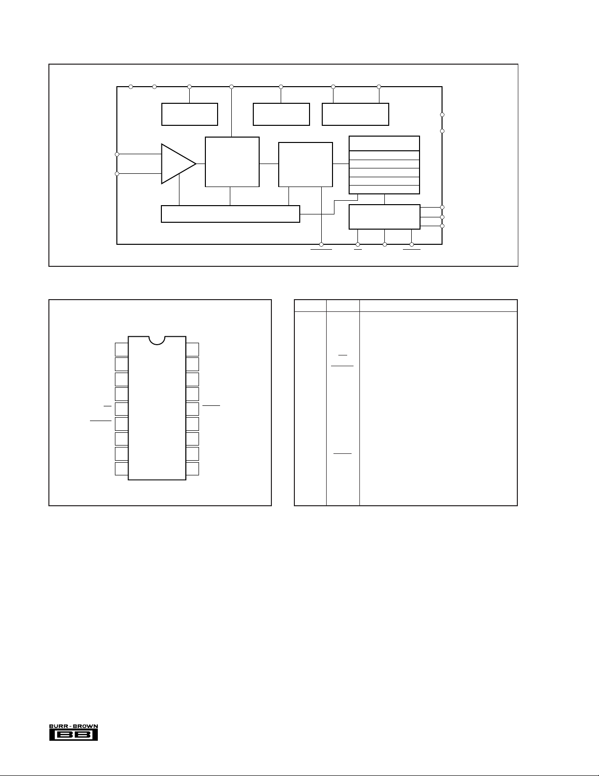
ADS1212 SIMPLIFIED BLOCK DIAGRAM
AGND AV
3
REF
DD
OUT
REF
IN
16 17 18 4 7 8
+2.5V
Reference
1
AINP
A
2
N
IN
PGA
Second-Order
∆Σ
Modulator
Modulator Control
ADS1212 PIN CONFIGURATION
TOP VIEW DIP/SOIC
A
IN
A
IN
AGND
V
BIAS
CS
DSYNC
X
X
OUT
DGND
1
P
2
N
3
4
ADS1212
5
6
7
IN
8
9
18
17
16
15
14
13
12
11
10
REF
IN
REF
OUT
AV
DD
MODE
DRDY
SDOUT
SDIO
SCLK
DV
DD
V
BIAS
+3.3V Bias
Generator
X
IN
Clock Generator
Third-Order
Digital Filter
65 1415
DSYNC CS DRDYMODE
ADS1212 PIN DEFINITIONS
PIN NO NAME DESCRIPTION
1A
2A
3 AGND Analog Ground.
4V
5 CS Chip Select Input.
6 DSYNC Control Input to Synchronize Serial Output Data.
7X
8X
9 DGND Digital Ground.
10 DV
11 SCLK Clock Input/Output for serial data transfer.
12 SDIO Serial Data Input (can also function as Serial Data
13 SDOUT Serial Data Output.
14 DRDY Data Ready.
15 MODE SCLK Control Input (Master = 1, Slave = 0).
16 AV
17 REF
18 REF
P Noninverting Input.
IN
N Inverting Input.
IN
BIAS
IN
OUT
DD
DD
OUT
IN
X
OUT
9
10
Micro Controller
Instruction Register
Command Register
Data Output Register
Offset Register
Full-Scale Register
11
Serial Interface
12
13
Bias Voltage Output, +3.3V nominal.
System Clock Input.
System Clock Output.
Digital Supply, +5V nominal.
Output).
Analog Supply, +5V nominal.
Reference Output, +2.5V nominal.
Reference Input.
DGND
DV
DD
SCLK
SDIO
SDOUT
®
ADS1212, 1213
4

ADS1213 SIMPLIFIED BLOCK DIAGRAM
AGND AV
REF
DD
OUT
REF
IN
6 19 20 21 7 10 11
+2.5V
4
A
1P
IN
5
A
1N
IN
2
A
2P
IN
3
A
2N
IN
A
3P
IN
A
3N
IN
A
4P
IN
A
4N
IN
MUX
24
1
22
23
Reference
PGA
Second-Order
∆∑
Modulator
Modulator Control
ADS1213P AND ADS1213U PIN CONFIGURATION
TOP VIEW DIP/SOIC
3N
A
IN
2P
A
IN
2N
A
IN
1P
A
IN
1N
A
IN
AGND
V
BIAS
CS
DSYNC
X
X
OUT
DGND
1
2
3
4
5
6
ADS1213P
7
ADS1213U
8
9
10
IN
11
12
24
23
22
21
20
19
18
17
16
15
14
13
A
3P
IN
4N
A
IN
4P
A
IN
REF
IN
REF
OUT
AV
DD
MODE
DRDY
SDOUT
SDIO
SCLK
DV
DD
V
BIAS
+3.3V Bias
Generator
X
IN
Clock Generator
X
OUT
12
13
Micro Controller
Third-Order
Digital Filter
Instruction Register
Command Register
Data Output Register
Offset Register
Full-Scale Register
14
Serial Interface
15
16
98 1718
DSYNC CS DRDYMODE
ADS1213P AND ADS1213U PIN DEFINITIONS
PIN NO NAME DESCRIPTION
1A
2A
3A
4A
5A
6 AGND Analog Ground.
7V
8 CS Chip Select Input.
9 DSYNC Control Input to Synchronize Serial Output Data.
10 X
11 X
12 DGND Digital Ground.
13 DV
14 SCLK Clock Input/Output for serial data transfer.
15 SDIO Serial Data Input (can also function as Serial Data
16 SDOUT Serial Data Output.
17 DRDY Data Ready.
18 MODE SCLK Control Input (Master = 1, Slave = 0).
19 AV
20 REF
21 REF
22 A
23 A
24 A
3N Inverting Input Channel 3.
IN
2P Noninverting Input Channel 2.
IN
2N Inverting Input Channel 2.
IN
1P Noninverting Input Channel 1.
IN
1N Inverting Input Channel 1.
IN
Bias Voltage Output, +3.3V nominal.
BIAS
System Clock Input.
IN
System Clock Output.
OUT
Digital Supply, +5V nominal.
DD
Output).
Analog Supply, +5V nominal.
DD
Reference Output: +2.5V nominal.
OUT
Reference Input.
IN
4P Noninverting Input Channel 4.
IN
4N Inverting Input Channel 4.
IN
3P Noninverting Input Channel 3.
IN
DGND
DV
DD
SCLK
SDIO
SDOUT
5 ADS1212, 1213
®
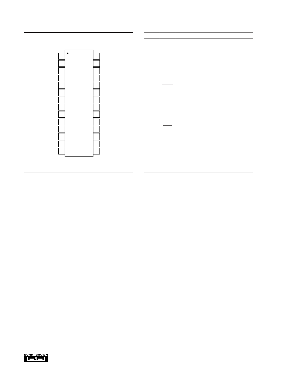
ADS1213E PIN CONFIGURATION
TOP VIEW SSOP
3N
A
IN
2P
A
IN
2N
A
IN
1P
A
IN
1N
A
IN
AGND
V
BIAS
NIC
NIC
CS
DSYNC
X
X
OUT
DGND
1
2
3
4
5
6
7
ADS1213E
8
9
10
11
12
IN
13
14
28
27
26
25
24
23
22
21
20
19
18
17
16
15
A
3P
IN
4N
A
IN
4P
A
IN
REF
IN
REF
OUT
AV
DD
MODE
NIC
NIC
DRDY
SDOUT
SDIO
SCLK
DV
DD
ADS1213E PIN DEFINITIONS
PIN NO NAME DESCRIPTION
1A
2A
3A
4A
5A
6 AGND Analog Ground.
7V
8 NIC Not Internally Connected.
9 NIC Not Internally Connected.
10 CS Chip Select Input.
11 DSYNC Control Input to Synchronize Serial Output Data.
12 X
13 X
14 DGND Digital Ground.
15 DV
16 SCLK Clock Input/Output for serial data transfer.
17 SDIO Serial Data Input (can also function as Serial Data
18 SDOUT Serial Data Output.
19 DRDY Data Ready.
20 NIC Not Internally Connected.
21 NIC Not Internally Connected.
22 MODE SCLK Control Input (Master = 1, Slave = 0).
23 AV
24 REF
25 REF
26 A
27 A
28 A
3N Inverting Input Channel 3.
IN
2P Noninverting Input Channel 2.
IN
2N Inverting Input Channel 2.
IN
1P Noninverting Input Channel 1.
IN
1N Inverting Input Channel 1.
IN
Bias Voltage Output, +3.3V nominal.
BIAS
System Clock Input.
IN
System Clock Output.
OUT
Digital Supply, +5V nominal.
DD
Output).
Analog Supply, +5V nominal.
DD
Reference Output: +2.5V nominal.
OUT
Reference Input.
IN
4P Noninverting Input Channel 4.
IN
4N Inverting Input Channel 4.
IN
3P Noninverting Input Channel 3.
IN
®
ADS1212, 1213
6
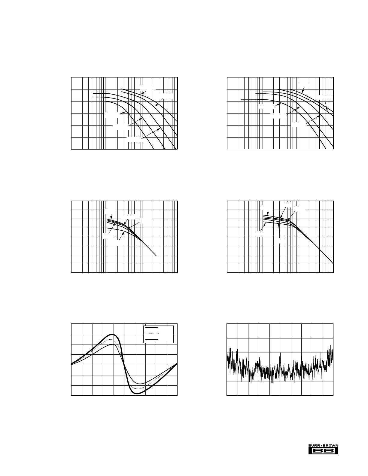
TYPICAL PERFORMANCE CURVES
RMS NOISE vs INPUT VOLTAGE LEVEL
(60Hz Data Rate)
Analog Input Differential Voltage (V)
–5.0 –4.0 –3.0 –2.0 –1.0 0 1.0 2.0 3.0 4.0 5.0
RMS Noise (ppm)
14
12
10
8
6
4
At TA = +25°C, AVDD = DV
2.5V reference, unless otherwise noted.
DD =
+5V, f
= 1MHz, programmable gain amplifier setting of 1, Turbo Mode Rate of 1, REF
XIN
disabled, V
OUT
disabled, and external
BIAS
EFFECTIVE RESOLUTION vs DATA RATE
24
22
20
18
16
14
Effective Resolution in Bits (rms)
12
1 10 100 1k
EFFECTIVE RESOLUTION vs DATA RATE
24
22
20
18
16
14
12
10
Effective Resolution in Bits (rms)
8
1 10 100 1k
(1MHz Clock)
Turbo 1
Turbo 2
Data Rate (Hz)
(1MHz Clock)
PGA 1
PGA 2
PGA 16
Data Rate (Hz)
Turbo 4
PGA 4
Turbo 16
PGA 8
Turbo 8
EFFECTIVE RESOLUTION vs DATA RATE
24
22
20
18
16
14
Effective Resolution in Bits (rms)
12
1 10 100 1k
EFFECTIVE RESOLUTION vs DATA RATE
24
22
20
18
16
14
12
10
Effective Resolution in Bits (rms)
8
1 10 100 1k
Turbo 1
PGA 1
PGA 16
(2.5MHz Clock)
Turbo 2
Data Rate (Hz)
(2.5MHz Clock)
PGA 2
PGA 8
Data Rate (Hz)
Turbo 16
Turbo 4
PGA 4
Turbo 8
LINEARITY vs TEMPERATURE
8
6
4
2
0
–2
Integral Nonlinearity (ppm)
–4
–6
–5 –4 –3 –2 –1 0 1 2 3 4 5
Analog Input Differential Voltage (V)
(60Hz Data Rate)
–40°C
+25°C
+85°C
®
7 ADS1212, 1213
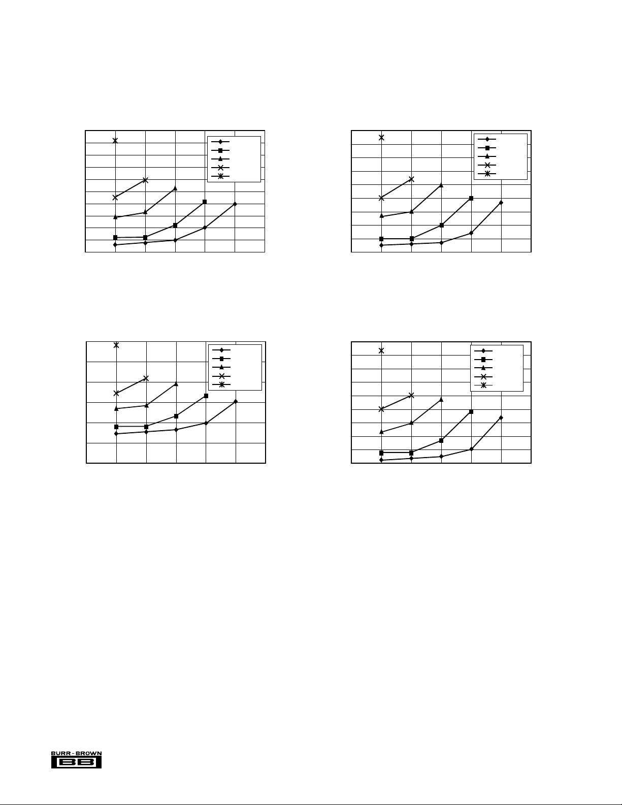
TYPICAL PERFORMANCE CURVES (CONT)
At TA = +25°C, AVDD = DV
2.5V reference, unless otherwise noted.
DD =
+5V, f
= 1MHz, programmable gain amplifier setting of 1, Turbo Mode Rate of 1, REF
XIN
disabled, V
OUT
disabled, and external
BIAS
POWER DISSIPATION vs PGA SETTING
15
14.5
14
13.5
13
12.5
12
11.5
Power Dissipation (mW)
11
10.5
10
124816
POWER DISSIPATION vs PGA SETTING
(External Reference; REF
6
5
4
3
2
Power Dissipation (mW)
1
0
124816
(REF
OUT
PGA Setting
PGA Setting
Enabled)
OUT
Disabled)
Turbo 1
Turbo 2
Turbo 4
Turbo 8
Turbo 16
Turbo 1
Turbo 2
Turbo 4
Turbo 8
Turbo 16
2700
2600
2500
2400
(µA)
2300
DD
2200
2100
Analog I
2000
1900
1800
980
880
780
680
(µA)
580
DD
480
380
Analog I
280
180
80
ANALOG CURRENT vs PGA SETTING
Enabled)
(REF
OUT
Turbo 1
Turbo 2
Turbo 4
Turbo 8
Turbo 16
124816
PGA Setting
ANALOG CURRENT vs PGA SETTING
(External Reference; REF
Disabled)
OUT
Turbo 1
Turbo 2
Turbo 4
Turbo 8
Turbo 16
124816
PGA Setting
®
ADS1212, 1213
8

THEORY OF OPERATION
The ADS1212 and ADS1213 are precision, high dynamic
range, self-calibrating, 24-bit, delta-sigma A/D converters
capable of achieving very high resolution digital results.
Each contains a programmable gain amplifier (PGA); a
second-order delta-sigma modulator; a programmable digital filter; a microcontroller including the Instruction, Command and Calibration registers; a serial interface; a clock
generator circuit; and an internal 2.5V reference. The
ADS1213 includes a 4-channel input multiplexer.
In order to provide low system noise, common-mode rejection of 100dB and excellent power supply rejection, the
design topology is based on a fully differential switched
capacitor architecture. Turbo Mode, a unique feature of the
ADS1212/13, can be used to boost the sampling rate of the
input capacitor, which is normally 7.8kHz with a 1MHz
clock. By programming the Command Register, the sampling rate can be increased to 15.6kHz, 31.2kHz, 62.5kHz,
or 125kHz. Each increase in sample rate results in an
increase in performance when maintaining the same output
data rate.
The programmable gain amplifier (PGA) of the ADS1212/
13 can be set to a gain of 1, 2, 4, 8 or 16—substantially
increasing the dynamic range of the converter and simplifying the interface to the more common transducers (see Table
I). This gain is implemented by increasing the number of
samples taken by the input capacitor from 7.8kHz for a gain
of 1 to 125kHz for a gain of 16. Since the Turbo Mode and
PGA functions are both implemented by varying the sampling frequency of the input capacitor, the combination of
PGA gain and Turbo Mode Rate is limited to 16 (see Table
II). For example, when using a Turbo Mode Rate of 8
(62.5kHz at 1MHz), the maximum PGA gain setting is 2.
ANALOG ANALOG INPUT
(1)
INPUT
FULL- EXAMPLE FULL- EXAMPLE
GAIN RANGE RANGE
SETTING (V) (V) (V) (V)
1 10 0 to 5 40 ±10
2 5 1.25 to 3.75 20 ±5
4 2.5 1.88 to 3.13 10 ±2.5
8 1.25 2.19 to 2.81 5 ±1.25
16 0.625 2.34 to 2.66 2.5 ±0.625
NOTE: (1) With a 2.5V reference, such as the internal reference. (2) This
example utilizes the circuit in Figure 12. Other input ranges are possible. (3)
The ADS1212/13 allows common-mode voltage as long as the absolute
input voltage on A
SCALE VOLTAGE SCALE VOLTAGE
P or AINN does not go below AGND or above AVDD.
IN
UTILIZING V
(3)
RANGE RANGE
TABLE I. Full-Scale Range vs PGA Setting.
TURBO MODE RATE AVAILABLE PGA SETTINGS
1 1, 2, 4, 8, 16
2 1, 2, 4, 8
4 1, 2, 4
8 1, 2
16 1
BIAS
(1,2)
(3)
The output data rate of the ADS1212/13 can be varied from
less than 1Hz to as much as 6.25kHz, trading off lower
resolution results for higher data rates. In addition, the data
rate determines the first null of the digital filter and sets the
–3dB point of the input bandwidth (see the Digital Filter
section). Changing the data rate of the ADS1212/13 does not
result in a change in the sampling rate of the input capacitor.
The data rate effectively sets the number of samples which
are used by the digital filter to obtain each conversion result.
A lower data rate results in higher resolution, lower input
bandwidth, and different notch frequencies than a higher
data rate. It does not result in any change in input impedance
or modulator frequency, or any appreciable change in power
consumption.
The ADS1212/13 also includes complete on-board calibration that can correct for internal offset and gain errors or
limited external system errors. Internal calibration can be
run when needed, or automatically and continuously in the
background. System calibration can be run as needed and the
appropriate input voltages must be provided to the ADS1212/
13. For this reason, there is no continuous system calibration
mode. The calibration registers are fully readable and writable. This feature allows for switching between various
configurations—different data rates, Turbo Mode Rates, and
gain settings—without re-calibrating.
The various settings, rates, modes, and registers of the
ADS1212/13 are read or written via a synchronous serial
interface. This interface can operate in either a self-clocked
mode (Master Mode) or an externally clocked mode (Slave
Mode). In the Master Mode, the serial clock (SCLK) frequency is one-quarter of the ADS1212/13 X
clock fre-
IN
quency.
The high resolution and flexibility of the ADS1212/13 allow
these converters to fill a wide variety of A/D conversion
tasks. In order to ensure that a particular configuration will
meet the design goals, there are several important items
which must be considered. These include (but are certainly
not limited to) the needed resolution, required linearity,
desired input bandwidth, power consumption goal, and sensor output voltage.
The remainder of this data sheet discusses the operation of
the ADS1212/13 in detail. In order to allow for easier
comparison of different configurations, “effective resolution” is used as the figure of merit for most tables and
graphs. For example, Table III shows a comparison between
data rate (and –3dB input bandwidth) versus PGA setting at
a Turbo Mode Rate of 1 and a clock rate of 1MHz. See the
Definition of Terms section for a definition of effective
resolution.
TABLE II. Available PGA Settings vs Turbo Mode Rate.
®
9 ADS1212, 1213

DATA -3DB
RATE FREQUENCY
(HZ) (HZ) G = 1 G = 2 G = 4 G = 8 G = 16
10 2.62 20 20 20 19 18
25 6.55 19 19 19 18 18
30 7.86 19 19 18 18 17
50 13.1 17 17 17 17 16
60 15.7 17 17 17 16 16
100 26.2 15 15 15 15 15
250 65.5 12 12 12 12 12
EFFECTIVE RESOLUTION (BITS RMS)
TABLE III. Effective Resolution vs Data Rate and Gain
Setting. (Turbo Mode Rate of 1 and a 1MHz
clock.)
DEFINITION OF TERMS
An attempt has been made to be consistent with the terminology used in this data sheet. In that regard, the definition
of each term is given as follows:
Analog Input Differential Voltage—For an analog signal
that is fully differential, the voltage range can be compared
to that of an instrumentation amplifier. For example, if both
analog inputs of the ADS1212 are at 2.5V, then the differential voltage is 0V. If one is at 0V and the other at 5V, then
the differential voltage magnitude is 5V. But, this is the case
regardless of which input is at 0V and which is at 5V, while
the digital output result is quite different.
The analog input differential voltage is given by the following equation: A
P – AINN. Thus, a positive digital output is
IN
produced whenever the analog input differential voltage is
positive, while a negative digital output is produced whenever the differential is negative.
For example, when the converter is configured with a 2.5V
reference and placed in a gain setting of 2, the positive fullscale output is produced when the analog input differential
is 2.5V. The negative full-scale output is produced when the
differential is –2.5V. In each case, the actual input voltages
must remain within the AGND to AV
range (see Table I).
DD
Actual Analog Input Voltage—The voltage at any one
analog input relative to AGND.
Full-Scale Range (FSR)—As with most A/D converters,
the full-scale range of the ADS1212/13 is defined as the
“input” which produces the positive full-scale digital output
minus the “input” which produces the negative full-scale
digital output.
For example, when the converter is configured with a 2.5V
reference and is placed in a gain setting of 2, the full-scale
range is: [2.5V (positive full scale) minus –2.5V (negative
full scale)] = 5V.
Typical Analog Input Voltage Range—This term describes the actual voltage range of the analog inputs which
will cover the converter’s full-scale range, assuming that
each input has a common-mode voltage that is greater than
/PGA and smaller than (AVDD – REFIN/PGA).
REF
IN
For example, when the converter is configured with a
2.5V reference and placed in a gain setting of 2, the
typical input voltage range is 1.25V to 3.75V (commonmode voltage = 2.5V). However, an input range of 0V to
2.5V (common-mode voltage = 1.25V) or 2.5V to 5V
(common-mode voltage = 3.75V) would also cover the
converter’s full-scale range.
Voltage Span—This is simply the magnitude of the typical
analog input voltage range. For example, when the converter
is configured with a 2.5V reference and placed in a gain
setting of 2, the input voltage span is 2.5V.
Least Significant Bit (LSB) Weight—This is the theoretical amount of voltage that the differential voltage at the
analog input would have to change in order to observe a
change in the output data of one least significant bit. It is
computed as follows:
LSB Weight =
Full−Scale Range
N
2
where N is the number of bits in the digital output.
Effective Resolution—The effective resolution of the
ADS1212/13 in a particular configuration can be expressed
in two different units: bits rms (referenced to output) and
microvolts rms (referenced to input). Computed directly
from the converter’s output data, each is a statistical calculation based on a given number of results. Knowing one, the
other can be computed as follows:
10V
ER in bits rms =
ER in Vrms =
20•log
PGA
ER in Vrms
6. 02
10V
PGA
6. 02•ER in bits rms +1.76
10
20
−1.76
The 10V figure in each calculation represents the full-scale
range of the ADS1212/13 in a gain setting of 1. This means
that both units are absolute expressions of resolution—the
performance in different configurations can be directly compared regardless of the units. Comparing the resolution of
different gain settings expressed in bits rms requires accounting for the PGA setting.
Main Controller—A generic term for the external
microcontroller, microprocessor, or digital signal processor
which is controlling the operation of the ADS1212/13 and
receiving the output data.
®
ADS1212, 1213
10
f
FILTER RESPONSE
Frequency (Hz)
–40
–60
–80
–100
–120
–140
–160
55 56 57 58 59 60 61 62 63 64 65
FILTER RESPONSE
Frequency (Hz)
0
–20
–40
–60
–80
–100
–120
–140
–160
0 50 100 150 200 250 300
Gain (dB) Gain (dB)
—The frequency of the crystal oscillator or CMOS
XIN
compatible input signal at the X
—The frequency or speed at which the modulator of the
f
MOD
input of the ADS1212/13.
IN
ADS1212/13 is running, given by the following equation:
f
•Turbo Mode
f
MOD
f
—The frequency or switching speed of the input
SAMP
XIN
=
128
sampling capacitor. The value is given by the following
equation:
f
•Turbo Mode •Gain Setting
XIN
=
128
—The frequency of the digital output data
f
DATA
, t
f
SAMP
DATA
produced by the ADS1212/13 or the inverse of this (the
period), respectively, f
f
f
DATA
=
XIN
128 • Decimation Ratio +1
()
is also referred to as the data rate.
DATA
• Turbo Mode
,t
DATA
1
=
f
DATA
Conversion Cycle—The term “conversion cycle” usually
refers to a discrete A/D conversion operation, such as that
performed by a successive approximation converter. As
used here, a conversion cycle refers to the t
time period.
DATA
However, each digital output is actually based on the modulator results from the last three t
time periods.
DATA
DIGITAL FILTER
The digital filter of the ADS1212/13 computes the output
result based on the most recent results from the delta-sigma
modulator. The number of modulator results that are used
depend on the decimation ratio set in the Command Register. At the most basic level, the digital filter can be thought
of as simply averaging the modulator results and presenting
this average as the digital output.
While the decimation ratio determines the number of modulator results to use, the modulator runs faster at higher Turbo
Modes. These two items, together with the ADS1212/13
clock frequency, determine the output data rate:
0
–20
–40
–60
–80
Gain (dB)
–100
–120
–140
–160
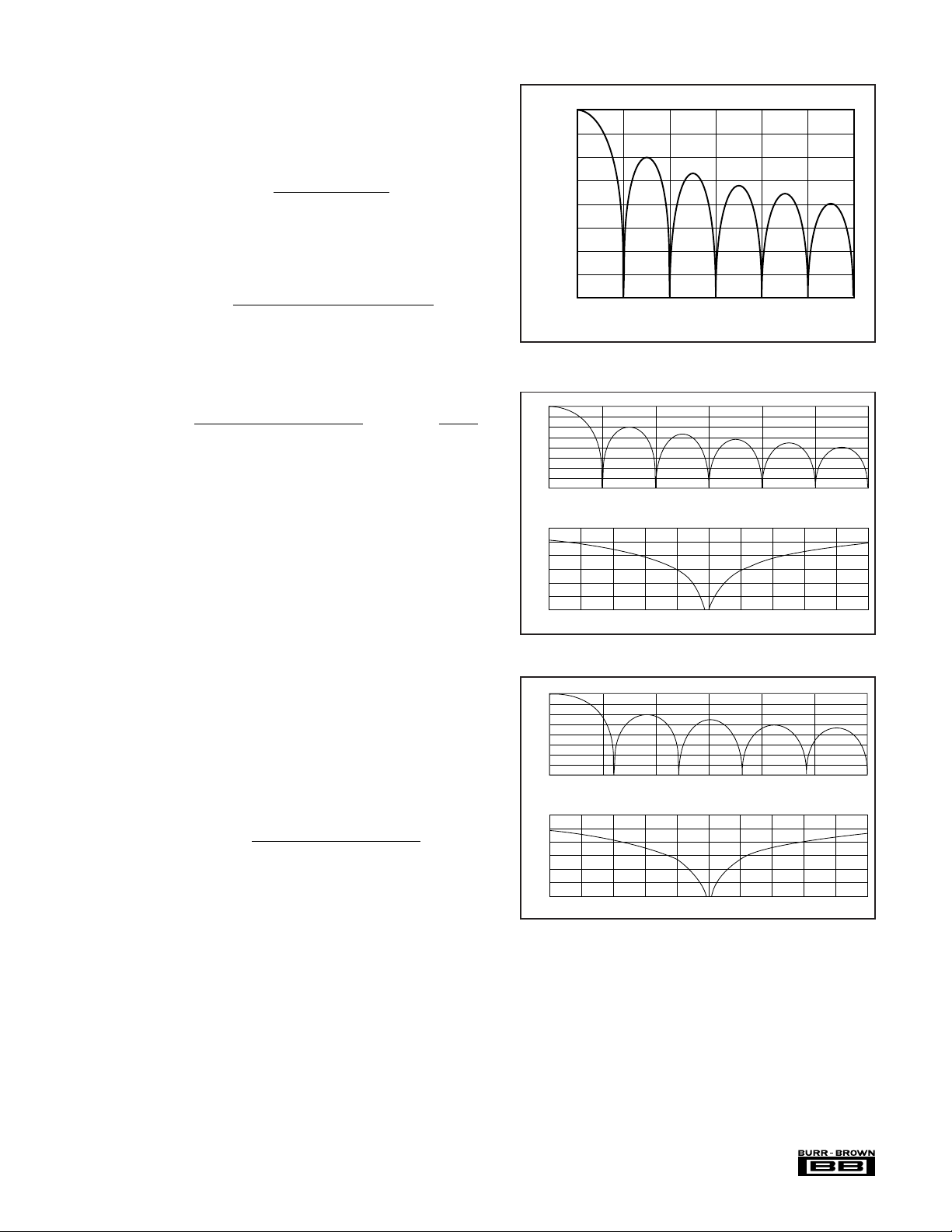
NORMALIZED DIGITAL FILTER RESPONSE
0123456
Frequency (Hz)
FIGURE 1. Normalized Digital Filter Response.
0
–20
–40
–60
–80
–100
Gain (dB)
–120
–140
–160
0 50 100 150 200 250 300
–40
–60
–80
–100
Gain (dB)
–120
–140
–160
45 46 47 48 49 50 51 52 53 54 55
FILTER RESPONSE
Frequency (Hz)
FILTER RESPONSE
Frequency (Hz)
FIGURE 2. Digital Filter Response at a Data Rate of 50Hz.
f
f
DATA
=
XIN
128• Decimation Ratio +1
()
Also, since the conversion result is essentially an average,
the data rate determines where the resulting notches are in
the digital filter. For example, if the output data rate is 1kHz,
then a 1kHz input frequency will average to zero during the
1ms conversion cycle. Likewise, a 2kHz input frequency
will average to zero, etc.
In this manner, the data rate can be used to set specific notch
frequencies in the digital filter response (see Figure 1 for the
normalized response of the digital filter). For example, if the
rejection of power line frequencies is desired, then the data
rate can simply be set to the power line frequency. Figures
2 and 3 show the digital filter response for a data rate of
50Hz and 60Hz, respectively.
•Turbo Mode
FIGURE 3. Digital Filter Response at a Data Rate of 60Hz.
If the effective resolution at a 50Hz or 60Hz data rate is not
adequate for the particular application, then power line frequencies could still be rejected by operating the ADS1212/13
at 25/30Hz, 16.7/20Hz, 12.5/15Hz, etc. If a higher data rate
is needed, then power line frequencies must either be rejected
before conversion (with an analog notch filter) or after
conversion (with a digital notch filter running on the main
controller).
®
11 ADS1212, 1213
Filter Equation
The digital filter is described by the following transfer
function:
|H(f)|=
sin
N •sin
π•f•N
f
MOD
π•f
f
MOD
3
where N is the Decimation Ratio.
3
This filter has a (sin(x)/x)
response and is referred to a sinc
filter. For the ADS1212/13, this type of filter allows the data
rate to be changed over a very wide range (nearly four orders
of magnitude). However, the –3dB point of the filter is 0.262
times the data rate. And, as can be seen in Figures 1 and 2,
the rejection in the stopband (frequencies higher than the
first notch frequency) may only be –40dB.
These factors must be considered in the overall system
design. For example, with a 50Hz data rate, a significant
signal at 75Hz may alias back into the passband at 25Hz.
The analog front end can be designed to provide the needed
attenuation to prevent aliasing, or the system may simply
provide this inherently. Another possibility is increasing the
data rate and then post filtering with a digital filter on the
main controller.
Filter Settling
The number of modulator results used to compute each
conversion result is three times the Decimation Ratio. This
means that any step change (or any channel change for the
ADS1213) will require at least three conversions to fully
settle. However, if the change occurs asynchronously, then at
least four conversions are required to ensure complete settling. For example, on the ADS1213, the fourth conversion
result after a channel change will be valid (see Figure 4).
the effective resolution of the output data at a given data rate,
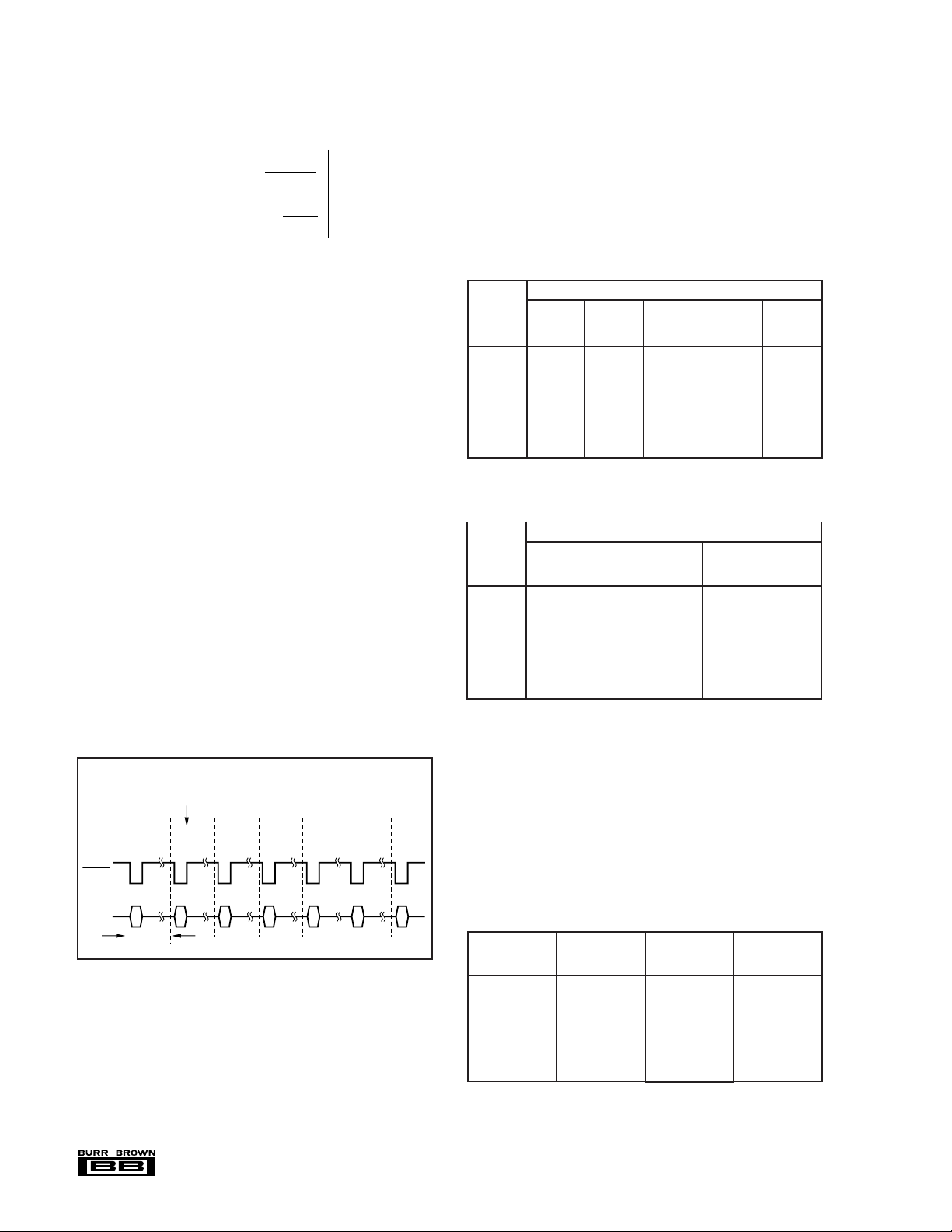
but there is also an increase in power dissipation. For Turbo
Mode Rates 2 and 4, the increase is slight. For rates 8 and
16, the increase is more substantial. See the Typical Performance Curves for more information.
In a Turbo Mode Rate of 16, the ADS1212/13 can offer 16
bits of effective resolution at a 1kHz data rate. A comparison
of effective resolution versus Turbo Mode Rates and output
data rates is shown in Table IV while Table V shows the
corresponding noise level in µVrms.
3
Data Turbo Turbo Turbo Turbo Turbo
Rate Mode Mode Mode Mode Mode
(Hz) Rate 1 Rate 2 Rate 4 Rate 8 Rate 16
10 20 21 21
20 19 20 21 21
40 18 20 21 21 21
50 17 19 20 21 21
60 17 19 20 21 21
100 15 17 19 21 21
250 12 14 16 19 20
1000 12 14 16
Effective Resolution (Bits rms)
TABLE IV. Effective Resolution vs Data Rate and Turbo Mode
Rate. (Gain setting of 1 and 1MHz clock.)
NOISE LEVEL (µVrms)
DATA TURBO TURBO TURBO TURBO TURBO
RATE MODE MODE MODE MODE MODE
(Hz) RATE 1 RATE 2 RATE 4 RATE 8 RATE 16
10 7.6 3.8 3.8
20 15 7.6 3.8 3.8
40 30 7.6 3.8 3.8 3.8
50 60 15 7.6 3.8 3.8
60 60 15 7.6 3.8 3.8
100 240 60 15 3.8 3.8
250 1900 480 120 15 7.6
1000 1900 480 120
TABLE V. Noise Level vs Data Rate and Turbo Mode Rate.
(Gain setting of 1 and 1MHz clock.)
Significant Analog Input Change
ADS1213 Channel Change
Valid
Data
DRDY
Serial
I/O
t
DATA
or
Valid
Data
Data
not
Valid
Data
not
Valid
Data
not
Valid
Valid
Data
Valid
Data
FIGURE 4. Asynchronous ADS1212/13 Analog Input Volt-
age Step or ADS1213 Channel Change to Fully
Settled Output Data.
TURBO MODE
The ADS1212/13 offers a unique Turbo Mode feature which
can be used to increase the modulator sampling rate by 2, 4,
8, or 16 times normal. With the increase of modulator
sampling frequency, there can be a substantial increase in
®
ADS1212, 1213
The Turbo Mode feature allows trade-offs to be made
between the ADS1212/13 X
clock frequency, power dissi-
IN
pation, and effective resolution. If a 0.5MHz clock is available but a 1MHz clock is needed to achieve the desired
performance, a Turbo Mode Rate of 2X will result in the
same effective resolution. Table VI provides a comparison
of effective resolution at various clock frequencies, data
rates, and Turbo Mode Rates.
DATA XIN CLOCK TURBO EFFECTIVE
RATE FREQUENCY MODE RESOLUTION
(Hz) (MH z) RATE (B its rms)
60 2 2 20
60 1 4 20
60 0.5 8 20
100 2 2 19
100 1 4 19
100 0.5 8 19
TABLE VI. Effective Resolution vs Data Rate, Clock
Frequency, and Turbo Mode Rate. (Gain setting of 1.)
12

The Turbo Mode Rate (TMR) is programmed via the Sampling Frequency bits of the Command Register. Due to the
increase in input capacitor sampling frequency, higher Turbo
Mode settings result in lower analog input impedance;
A
Impedance (Ω) = (1MHz/f
IN
)•20E6/(G•TMR)
XIN
where G is the gain setting. Because the modulator rate also
changes in direct relation to the Turbo Mode setting, higher
values result in a lower impedance for the REF
Impedance (Ω) = (1MHz/f
REF
IN
XIN
input:
IN
)•5E6/TMR
The Turbo Mode Rate can be set to 1, 2, 4, 8, or 16. Consult
the graphs shown in the Typical Performance Curves for full
details on the performance of the ADS1212/13 operating in
different Turbo Mode Rates. Keep in mind that higher Turbo
Mode Rates result in fewer available gain settings as shown
in Table II.
PROGRAMMABLE GAIN AMPLIFIER
The programmable gain amplifier gain setting is programmed
via the PGA Gain bits of the Command Register. Changes
in the gain setting (G) of the programmable gain amplifier
results in an increase in the input capacitor sampling frequency. Thus, higher gain settings result in a lower analog
input impedance:
Impedance (Ω) = (1MHz/f
A
IN
)•20E6/(G•TMR)
XIN
where TMR is the Turbo Mode Rate. Because the modulator
speed does not depend on the gain setting, the input impedance seen at REF
does not change.
IN
The PGA can be set to gains of 1, 2, 4, 8, or 16. These gain
settings with their resulting full-scale range and typical
voltage range are shown in Table I. Keep in mind that higher
Turbo Mode Rates result in fewer available gain settings as
shown in Table II.
SOFTWARE GAIN
The excellent performance, flexibility, and low cost of the
ADS1212/13 allow the converter to be considered for designs which would not normally need a 24-bit ADC. For
example, many designs utilize a 12-bit converter and a highgain INA or PGA for digitizing low amplitude signals. For
some of these cases, the ADS1212/13 by itself may be a
solution, even though the maximum gain is limited to 16.
To get around the gain limitation, the digital result can
simply be shifted up by “n” bits in the main controller—
resulting in a gain of “n” times G, where G is the gain
setting. While this type of manipulation of the output data
is obvious, it is easy to miss how much the gain can be
increased in this manner on a 24-bit converter.
For example, shifting the result up by three bits when the
ADS1212/13 is set to a gain of 16 results in an effective gain
of 128. At lower data rates, the converter can easily provide
more than 12 bits of resolution. Even higher gains are
possible. The limitation is a combination of the needed data
rate, desired noise performance, and desired linearity.
CALIBRATION
The ADS1212/13 offers several different types of calibration, and the particular calibration desired is programmed
via the Command Register. In the case of Background
Calibration, the calibration will repeat at regular intervals
indefinitely. For all others, the calibration is performed once
and then normal operation is resumed.
Each type of calibration is covered in detail in their respective section. In general, calibration is recommended immediately after power-on and whenever there is a “significant”
change in the operating environment. The amount of change
which should cause a re-calibration is dependent on the
application, effective resolution, etc. Where high accuracy is
important, re-calibration should be done on changes in
temperature and power supply. In all cases, re-calibration
should be done when the gain, Turbo Mode, or data rate is
changed.
After a calibration has been accomplished, the Offset Calibration Register and the Full-Scale Calibration Register
contain the results of the calibration. The data in these
registers are accurate to the effective resolution of the
ADS1212/13’s mode of operation during the calibration.
Thus, these values will show a variation (or noise) equivalent to a regular conversion result.
For those cases where this error must be reduced, it is
tempting to consider running the calibration at a slower data
rate and then increasing the converter’s data rate after the
calibration is complete. Unfortunately, this will not work as
expected. The reason is that the results calculated at the
slower data rate would not be valid for the higher data rate.
Instead, the calibration should be done repeatedly. After
each calibration, the results can be read and stored. After the
desired number of calibrations, the main controller can
compute an average and write this value into the calibration
registers. The resulting error in the calibration values will be
reduced by the square root of the number of calibrations
which were averaged.
The calibration registers can also be used to provide system
offset and gain corrections separate from those computed by
the ADS1212/13. For example, these might be burned into
2
PROM during final product testing. On power-on, the
E
main controller would load these values into the calibration
registers. A further possibility is a look-up table based on the
current temperature.
Note that the values in the calibration registers will vary from
configuration to configuration and from part to part. There is
no method of reliably computing what a particular calibration
register should be to correct for a given amount of system
error. It is possible to present the ADS1212/13 with a known
amount of error, perform a calibration, read the desired
calibration register, change the error value, perform another
calibration, read the new value and use these values to
interpolate an intermediate value.
13 ADS1212, 1213
®
 Loading...