Burr Brown Corporation DCP012415DP-U, ADS1201U-1K, ADS1201U Datasheet

ADS1201
®
©
1997 Burr-Brown Corporation PDS-1417C Printed in U.S.A. October, 1999
International Airport Industrial Park • Mailing Address: PO Box 11400, Tucson, AZ 85734 • Street Address: 6730 S. Tucson Blvd., Tucson, AZ 85706 • Tel: (520) 746-1111
Twx: 910-952-1111 • Internet: http://www.burr-brown.com/ • Cable: BBRCORP • Telex: 066-6491 • FAX: (520) 889-1510 • Immediate Product Info: (800) 548-6132
High Dynamic Range
DELTA-SIGMA MODULATOR
ADS1201
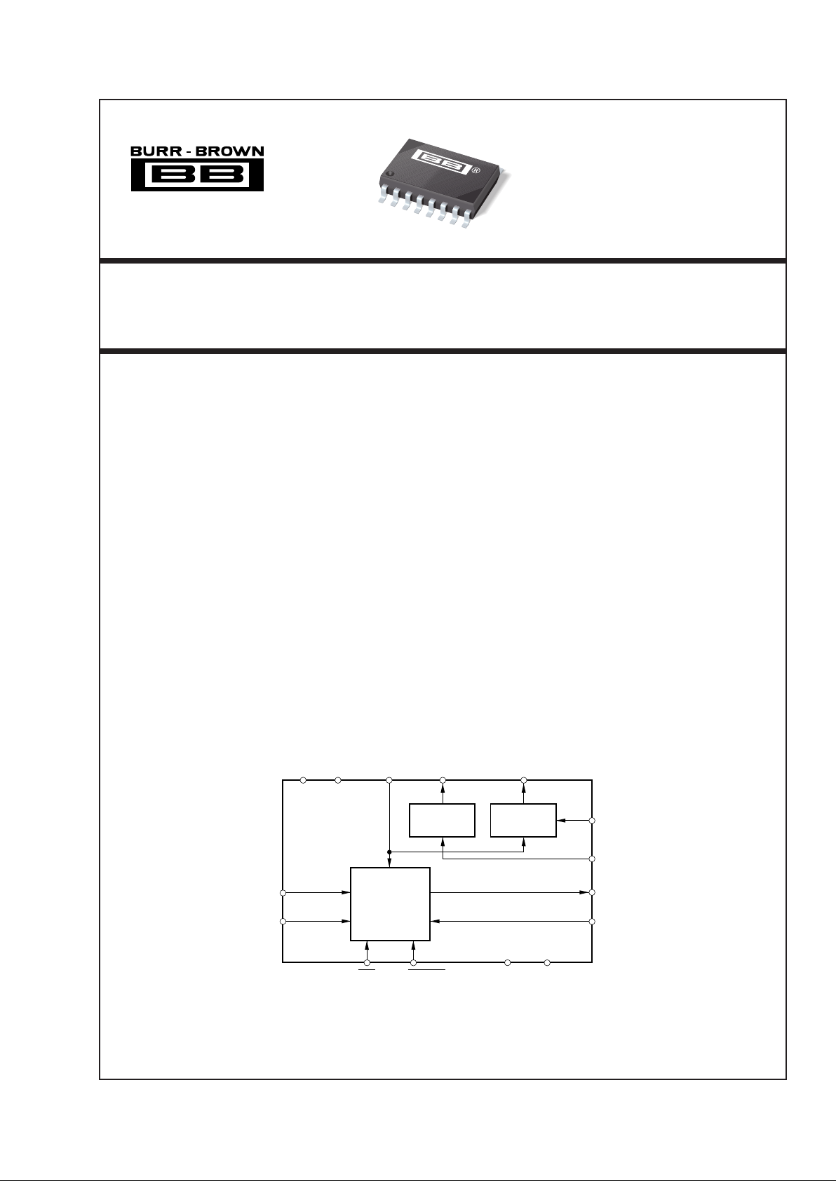
+2.5V
Reference
Bias
Generator
Second-Order
∆Σ
Modulator
AVDDAGND REF
OUT
REF
IN
V
BIAS
CAL GAIN/OFFSET DGNDDV
DD
AINP
A
IN
N
MOUT
BIAS
EN
REF
EN
MCLK
DESCRIPTION
The ADS1201 is a precision, 130dB dynamic range,
delta-sigma (∆Σ) modulator operating from a single
+5V supply. The differential inputs are ideal for direct
connection to transducers or low level signals. With
the appropriate digital filter and modulator rate, the
device can be used to achieve 24-bit analog-to-digital
(A/D) conversion with no missing codes. Effective
resolution of 20 bits can be maintained with a digital
filter bandwidth of 1kHz at a modulator rate of 320kHz.
The ADS1201 is designed for use in high resolution
measurement applications including smart transmitters, industrial process control, weigh scales, chromatography, and portable instrumentation. It is available
in a 16-lead SOIC package.
FEATURES
● 130dB DYNAMIC RANGE
● FULLY DIFFERENTIAL INPUT
● TWO-WIRE INTERFACE
● INTERNAL/EXTERNAL REFERENCE
● ON-CHIP SWITCHES FOR CALIBRATION
APPLICATIONS
● INDUSTRIAL PROCESS CONTROL
● INSTRUMENTATION
● SMART TRANSMITTERS
● PORTABLE INSTRUMENTS
● WEIGH SCALES
● PRESSURE TRANSDUCERS

2
ADS1201
®
At TA = +25°C, AVDD = DVDD = +5V, MCLK = 320kHz, REFEN LOW, BIASEN LOW, and external +2.5V reference, unless otherwise specified.
The information provided herein is believed to be reliable; however, BURR-BROWN assumes no responsibility for inaccuracies or omissions. BURR-BROWN assumes
no responsibility for the use of this information, and all use of such information shall be entirely at the user’s own risk. Prices and specifications are subject to change
without notice. No patent rights or licenses to any of the circuits described herein are implied or granted to any third party. BURR-BROWN does not authorize or warrant
any BURR-BROWN product for use in life support devices and/or systems.
SPECIFICATIONS
ADS1201U
PARAMETER CONDITIONS MIN TYP MAX UNITS
ANALOG INPUT
Absolute Input Voltage Range 0 +5 V
With V
BIAS
(1)
–10 +10 V
Differential Input Voltage Range –5 +5 V
With V
BIAS
(1)
–20 See Note 2 +20 V
Input Impedance 250
(4)
kΩ
Input Capacitance 8pF
Input Leakage Current 550pA
At T
MIN
to T
MAX
1nA
SYSTEM PERFORMANCE
Dynamic Range 10Hz Bandwidth
(5)
130
(6)
dB
60Hz Bandwidth
(5)
115
(6)
120
(6)
dB
1kHz Bandwidth
(5)
115
(6)
dB
Integral Linearity Error 60Hz Bandwidth
(5)
±0.0015 %FSR
1kHz Bandwidth
(5)
±0.0015 %FSR
Offset Error
(2)
See Note 7 µV
Offset Drift
(3)
1 µV/°C
Gain Error
(2)
See Note 7 ppm
Gain Error Drift
(3)
1 µV/°C
Common-Mode Rejection At DC 80 100 dB
Power Supply Rejection 80 dB
REFERENCE
Internal Reference (REF
OUT
) 2.4 2.5 2.6 V
Drift 25 ppm/°C
Noise 50 µVp-p
Load Current Source or Sink –1 1 mA
Output Impedance 2 Ω
External Reference (REF
IN
) 2.0 3.0 V
Load Current 2.5 µA
V
BIAS
Output Using Internal Reference 3.15 3.3 3.45 V
Drift 50 ppm/°C
Load Current 10 mA
DIGITAL INPUT/OUTPUT
Logic Family TTL Compatible CMOS
Logic Levels:
V
IH
(MCLK) IIH = +5µA 2.0 DV
DD
+0.3 V
V
IL
(MCLK) IIL = +5µA –0.3 0.8 V
V
OH
(MOUT) IOH = 2 TTL Loads 2.4 V
V
OL
(MOUT) IOL = 2 TTL Loads 0.4 V
MCLK Frequency 0.02 1 MHz
POWER SUPPLY REQUIREMENTS
Power Supply Voltage Specified Performance 4.75 5.25 V
Supply Current
Analog Current 4.6 mA
Digital Current 0.4 mA
Additional Analog Current
REF
OUT
Enabled No Load 1.6 mA
V
BIAS
Enabled No Load 1 mA
Total Power Dissipation REF
OUT
, V
BIAS
Disabled 25 40 mW
TEMPERATURE RANGE
Specified Performance –40 +85 °C
NOTES: (1) This range is set with external resistors and V
BIAS
(as described in the text). Other ranges are possible. (2) After the on-chip offset and gain
calibration functions have been employed. (3) Re-calibration can reduce these errors. (4) Input impedance changes with MCLK. (5) Assume brick wall digital
filter is used. (6) 20 Log (full scale/r ms noise). (7) After calibration, these errors will be of the order of the effective resolution.

3
®
ADS1201
Analog Input: Current................................................ ±100mA, Momentary
±10mA, Continuous
Voltage ................................... AGND –0.3V to AV
DD
+0.3V
AV
DD
to DVDD...........................................................................–0.3V to 6V
AV
DD
to AGND .........................................................................–0.3V to 6V
DV
DD
to DGND.........................................................................–0.3V to 6V
AGND to DGND ................................................................................ ±0.3V
REF
IN
Voltage to AGND............................................ –0.3V to AVDD +0.3V
Digital Input Voltage to DGND ..................................–0.3V to DV
DD
+0.3V
Digital Output Voltage to DGND ............................... –0.3V to DV
DD
+0.3V
Lead Temperature (soldering, 10s) .............................................. +300°C
Internal Power Dissipation ............................................................. 500mW
NOTE: (1) Stresses above those listed under “Absolute Maximum Ratings” may
cause permanent damage to the device. Exposure to absolute maximum
conditions for extended periods may affect device reliability.
ABSOLUTE MAXIMUM RATINGS
ELECTROSTATIC
DISCHARGE SENSITIVITY
This integrated circuit can be damaged by ESD. Burr-Brown
recommends that all integrated circuits be handled with
appropriate precautions. Failure to observe proper handling
and installation procedures can cause damage.
ESD damage can range from subtle performance degradation
to complete device failure. Precision integrated circuits may
be more susceptible to damage because very small parametric
changes could cause the device not to meet its published
specifications.
PACKAGE SPECIFIED
DRAWING TEMPERATURE PACKAGE ORDERING TRANSPORT
PRODUCT PACKAGE NUMBER RANGE MARKING NUMBER
(1)
MEDIA
ADS1201U SOL-16 211 –40°C to +85°C ADS1201U ADS1201U Rails
"""""ADS1201U/1K Tape and Reel
NOTE: (1) Models with a slash (/) are available only in Tape and Reel in the quantities indicated (e.g., /1K indicates 1000 devices per reel). Ordering 1000 pieces
of “ADS1201U/1K” will get a single 1000-piece Tape and Reel.
PACKAGE/ORDERING INFORMATION
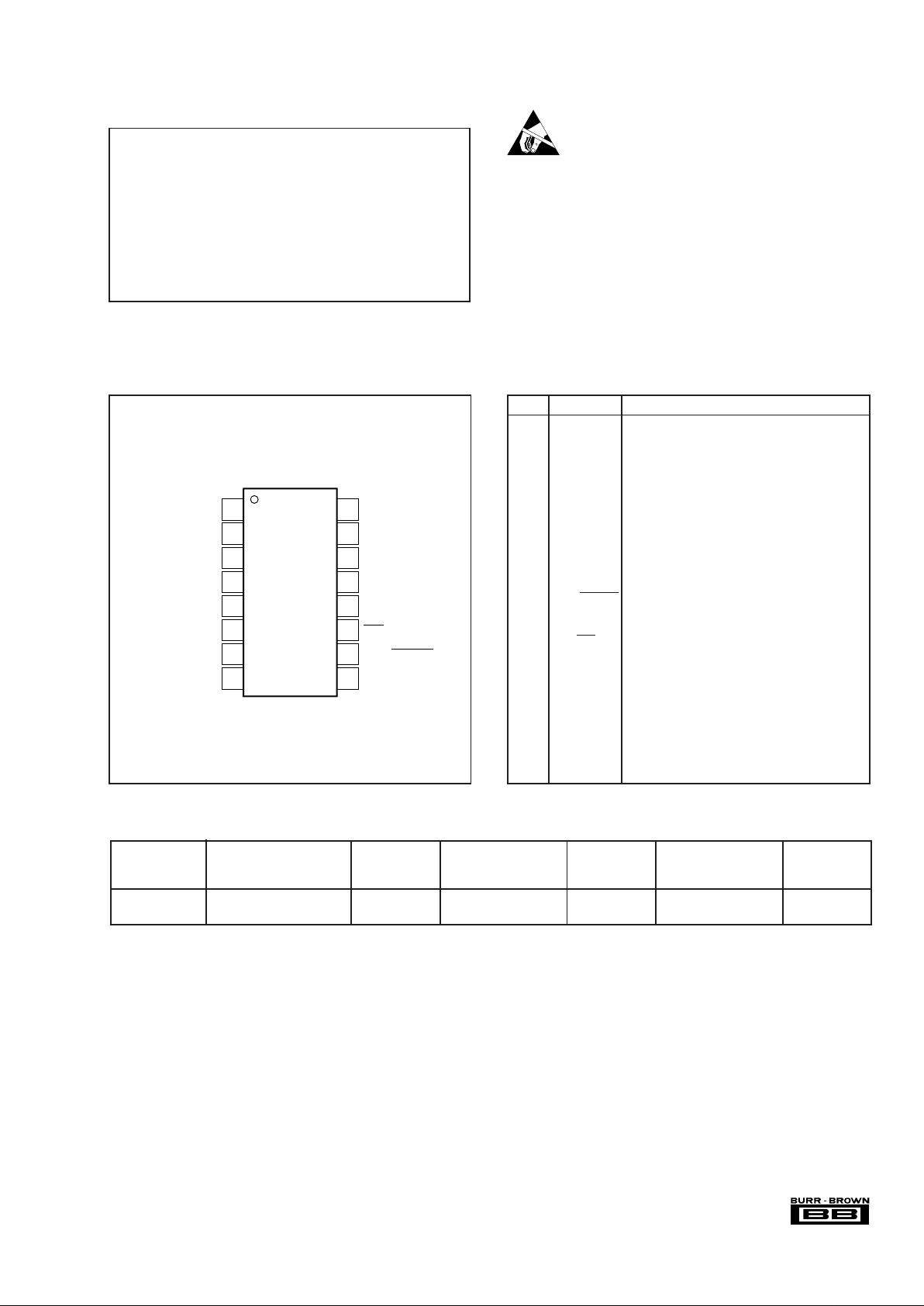
PIN CONFIGURATION
Top View SOIC
1AVDDAnalog Input: Analog Supply, +5V nominal.
2 REF
OUT
Analog Output: Internal Reference Voltage Output:
+2.5V nominal.
3 REF
IN
Analog Input: Reference Voltage Input.
4 NIC Not Internally Connected.
5A
IN
P Analog Input: Noninverting Input.
6A
IN
N Analog Input: Inverting Input.
7 AGND Analog Input: Analog Ground.
8V
BIAS
Analog Output: Bias Voltage Output, nominally
+3.3V (with +2.5V reference).
9 BIAS
EN
Digital Input: Bias Voltage Enable Input (HIGH =
enabled, LOW = disabled).
10
GAIN/OFFSET
Digital Input: Gain/Offset Calibration Select Input
(with CAL LOW; HIGH = gain configuration,
LOW = offset configuration).
11 CAL Digital Input: Calibration Control Input (HIGH =
normal operation, LOW = gain or offset
calibration configuration).
12 DGND Digital Input: Digital Ground.
13 DV
DD
Digital Input: Digital Supply, +5V nominal.
14 MCLK Digital Input: Modulator Clock Input. CMOS
compatible.
15 MOUT Digital Output: Modulator Output.
16 REF
EN
Digital Input: REF
OUT
Voltage Enable Input
(HIGH = enabled, LOW = disabled).
PIN DESCRIPTIONS
PIN NO
NAME DESCRIPTION
ADS1201
1
2
3
4
5
6
7
8
16
15
14
13
12
11
10
9
AV
DD
REF
OUT
REF
IN
NIC
A
IN
P
A
IN
N
AGND
V
BIAS
REF
EN
MOUT
MCLK
DV
DD
DGND
CAL
GAIN/OFFSET
BIAS
EN

4
ADS1201
®
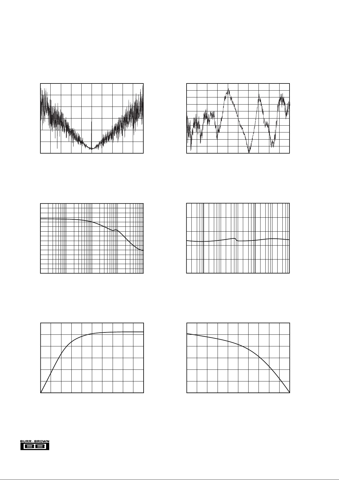
TYPICAL PERFORMANCE CURVES
At TA = +25°C, AVDD = DVDD = +5V, MCLK = 320kHz, REFEN LOW, BIASEN LOW, and external +2.5V reference, unless otherwise specified.
1.2
1
0.8
0.6
0.4
0.2
0
rms NOISE
V
DIN
(V)
–5–4–3–2–1012345
(ppm)
1.5
1.0
0.5
0
–0.5
–1.0
–1.5
–2.0
–2.5
–3.0
–3.5
LINEARITY
V
DIN
(V)
–5–4–3–2–1012345
(ppm)
110
105
100
95
CMRR vs FREQUENCY
Frequency (Hz)
0.1 1 10 100 1000
CMRR (dB)
70
68
66
64
62
60
PSRR vs FREQUENCY
Frequency (Hz)
0.1 1.0 10 100 1k 10k 100k
PSRR (dB)
30
25
20
15
10
5
0
TYPICAL SINK CURRENT
V
OL
(V)
0 0.5 1.0 1.5 2.0 2.5 3.0 3.5 4.0 4.5 5.0
I
OUT
(mA)
30
25
20
15
10
5
0
TYPICAL SOURCE CURRENT
V
OL
(V)
0 0.5 1.0 1.5 2.0 2.5 3.0 3.5 4.0 4.5 5.0
I
OUT
(mA)
 Loading...