Burr Brown Corporation ADC574ATH-BI, ADC574ATH, ADC574ASH-BI, ADC574ASH, ADC574AKP-BI Datasheet
...
®
ADC574A
FPO
Microprocessor-Compatible
ANALOG-TO-DIGITAL CONVERTER
FEATURES
● COMPLETE 12-BIT A/D CONVERTER WITH
REFERENCE, CLOCK, AND 8-, 12-, or 16BIT MICROPROCESSOR BUS INTERFACE
● IMPROVED PERFORMANCE SECOND
SOURCE FOR 574A-TYPE A/D
CONVERTERS
Conversion Time: 25
µs max
Bus Access Time: 150ns max
A
O
Input: Bus Contention During Read
Operation Eliminated
● DUAL IN-LINE PLASTIC, PLCC AND
HERMETIC CERAMIC
● FULLY SPECIFIED FOR OPERATION ON
±12V OR ±15V SUPPLIES
● NO MISSING CODES OVER
TEMPERATURE:
0
°C to +75°C: ADC574AJ and K Grades
–55
°C to +125°C: ADC574ASH, TH
DESCRIPTION
The ADC574A is a 12-bit successive approximation
analog-to-digital converter, utilizing state-of-the-art
CMOS and laser-trimmed bipolar die custom-designed
for freedom from latch-up and for optimum AC performance. It is complete with a self-contained +10V
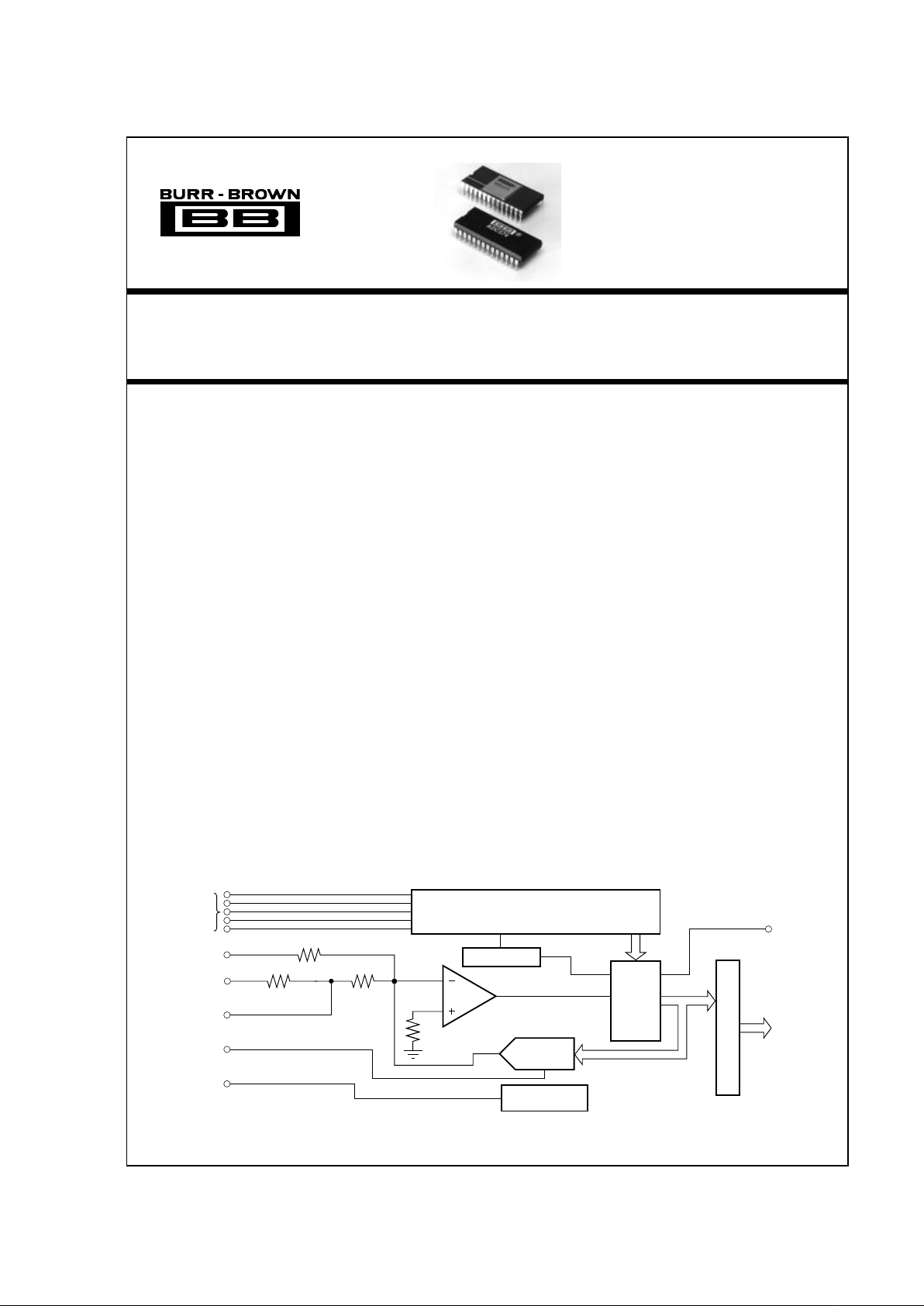
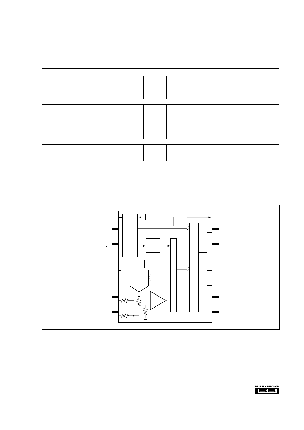
reference, internal clock, digital interface for microprocessor control, and three-state outputs.
The reference circuit, containing a buried zener, is lasertrimmed for minimum temperature coefficient. The
clock oscillator is current-controlled for excellent stability over temperature. Full-scale and offset errors may
be externally trimmed to zero. Internal scaling resistors
are provided for the selection of analog input signal
ranges of 0V to +10V, 0V to +20V, ±5V, and ±10V.
The converter may be externally programmed to provide 8- or 12-bit resolution. The conversion time for 12
bits is factory set for 25µs maximum.
Output data are available in a parallel format from TTLcompatible three-state output buffers. Output data are
coded in straight binary for unipolar input signals and
bipolar offset binary for bipolar input signals.
The ADC574A, available in both industrial and military
temperature ranges, requires supply voltages of +5V
and ±12V or ±15V. It is packaged in a 28-pin plastic
DIP, and a hermetic side-brazed ceramic DIP.
International Airport Industrial Park • Mailing Address: PO Box 11400 • Tucson, AZ 85734 • Street Address: 6730 S. Tucson Blvd. • Tucson, AZ 85706
Tel: (520) 746-1111 • Twx: 910-952-1111 • Cable: BBRCORP • Telex: 066-6491 • FAX: (520) 889-1510 • Immediate Product Info: (800) 548-6132
Successive
Approximation
Register
Control Logic
Comparator
12-Bit D/A
Converter
10V
Control
Inputs
Bipolar
Offset
20V Range
10V Range
Reference
Input
Reference
Output
Three-State Buffers
Status
Parallel
Data
Output
Clock
Reference
© 1984 Burr-Brown Corporation PDS-550G Printed in U.S.A., August, 1993

2
®
ADC574A
SPECIFICATIONS
ELECTRICAL
At TA = +25°C, VCC = +12V or +15V, VEE = –12V or –15V, and V
LOGIC
= +5V unless otherwise specified.
ADC574AJP, JH, SH ADC574AKP, KH, TH
PARAMETER MIN TYP MAX MIN TYP MAX UNITS
RESOLUTION 12 * Bits
INPUTS
ANALOG
Voltage Ranges: Unipolar 0 to +10, 0 to +20 * V
Bipolar ±5, ±10 * V
Impedance: 0 to +10V, ±5V 4.7 5 5.3 * * * kΩ
±10V, 0V to +20V 9.4 10 10.6 * * * kΩ
DIGITAL (CE, CS, R/C, A
O
, 12/8)
Over Temperature Range
Voltages: Logic 1 +2 +5.5 * * V
Logic 0 –0.5 +0.8 * * V
Current –5 0.1 +5 * * * µA
Capacitance 5 * pF
TRANSFER CHARACTERISTICS
ACCURACY
At +25°C
Linearity Error ±1 ±1/2 LSB
Unipolar Offset Error (Adjustable to Zero) ±2 * LSB
Bipolar Offset Error (Adjustable to Zero) ±10 ±4 LSB
Full-Scale Calibration Error
(1)
(Adjustable to Zero) ±0.25 * % of FS
(2)
No Missing Codes Resolution (Diff. Linearity) 11 12 Bits
Inherent Quantization Error ±1/2 * LSB
T
MIN
to T
MAX
Linearity Error: J, K Grades ±1 ±1/2 LSB
S, T Grades ±1 ±3/4 LSB
Full-Scale Calibration Error
Without Initial Adjustment
(1)
: J, K Grades ±0.47 ±0.37 % of FS
S, T Grades ±0.75 ±0.5 % of FS
Adjusted to Zero at +25°C: J, K Grades ±0.22 ±0.12 % of FS
S, T Grades ±0.5 ±0.25 % of FS
No Missing Codes Resolution (Diff. Linearity) 11 12 Bits
TEMPERATURE COEFFICIENTS (T
MIN
to T
MAX
)
(3)
Unipolar Offset: J, K Grades ±10 ±5 ppm/°C
S, T Grades ±5 ±2.5 ppm/°C
Max Change: All Grades ±2 ±1 LSB
Bipolar Offset: All Grades ±10 ±5 ppm/°C
Max Change: J, K Grades ±2 ±1 LSB
S, T Grades ±4 ±2 LSB
Full-Scale Calibration: J, K Grades ±45 ±25 ppm/°C
S, T Grades ±50 ±25 ppm/°C
Max Change: J, K Grades ±9 ±5 LSB
S, T Grades ±20 ±10 LSB
POWER SUPPLY SENSITIVITY
Change in Full-Scale Calibration
+13.5V < VCC < +16.5V or +11.4V < VCC < + 12.6V
±2 ±1 LSB
–16.5V < VEE < –13.5V or –12.6V < VEE < – 11.4V
±2 ±1 LSB
+4.5V < V
LOGIC
< +5.5V ±1/2 * LSB
CONVERSION TIME
(4)
8-Bit Cycle 10 13 17 * * * µ s
12-Bit Cycle 15 20 25 * • • µs
OUTPUTS
DIGITAL (DB
11
–DB0, STATUS)
(Over Temperature Range)
Output Codes: Unipolar Unipolar Straight Binary (USB)
Bipolar Bipolar Offset Binary (BOB)
Logic Levels: Logic 0 (I
SINK
= 1.6mA) +0.4 * V
Logic 1 (I
SOURCE
= 500µA) +2.4 * V
Leakage, Data Bits Only, High -Z State –5 0.1 +5 * * * µA
Capacitance 5 * pF

3
®
ADC574A
SPECIFICATIONS (CONT)
ELECTRICAL
At TA = +25°C, VCC = +12V or +15V, VEE = –12V or –15V, and V
LOGIC
= +5V unless otherwise specified.
ADC574AJP, JH, SH ADC574AKP, KH, TH
PARAMETERS MIN TYP MAX MIN TYP MAX UNITS
* Same specifications as ADC574AJP, AJH, ASH.
NOTES: (1) With fixed 50Ω resistor from REF OUT to REF IN. This parameter is also adjustable to zero at ±25°C (see Optional External Full Scale and Offset
Adjustments section). (2) FS in this specification table means Full Scale Range. That is, for a ±10V input range, FS means 20V; for a 0 to +10V range, FS means
10V. The term Full Scale for these specifications instead of Full-Scale Range is used to be consistent with other vendors' 574 and 574A type specifications tables.
(3) Using internal reference. (4) See Controlling the ADC574A section for detailed information concerning digital timing. (5) External loading must be constant during
conversion. The reference output requires no buffer amplifier with either ±12V or ±15V power supplies.
PIN CONFIGURATION
+5VDC Supply (V )
12/8
CS
A
R/C
CE
+V
Ref Out
Analog Common
Ref In
V
Bipolar Offset
10V Range
20V Range
Status
DB11 (MSB)
DB10
DB9
DB8
DB7
DB6
DB5
DB4
DB3
DB2
DB1
DB0 (LSB)
Digital Common
1
2
3
4
5
6
7
8
9
10
11
12
13
14
28
27
26
25
24
23
22
21
20
19
18
17
16
15
LOGIC
CC
EE
5kΩ
10kΩ
10V
Reference
12-Bit
D/A
Converter
Successive Approximation Register
Control
Logic
Power-up Reset
Clock
12 Bits
Comparator
12 Bits
Nibble ANibble BNibble C
Three-State Buffers and Control
O
5k
Ω
INTERNAL REFERENCE VOLTAGE
Voltage +9.9 +10.0 +10.1 * * * V
Source Current Available for External Loads
(5)
2.0 * mA
POWER SUPPLY REQUIREMENTS
Voltage: V
CC
+11.4 +16.5 * * V
V
EE
–11.4 –16.5 * * V
V
LOGIC
+4.5 +5.5 * * V
Current: I
CC
3.5 5 * * mA
I
EE
15 20 * * mA
I
LOGIC
915 * *mA
Power Dissipation (±15V Supplies) 325 450 * * mW
TEMPERATURE RANGE (Ambient: T
MIN
, T
MAX
)
Specifications: J, K Grades 0 +75 * * °C
S, T Grades –55 +125 * * °C
Storage –65 +150 * * °C
 Loading...