

Burr Brown PCM61P-J, PCM61P-K, PCM61P-P Datasheet
®
PCM61P
1
©
1989 Burr-Brown Corporation PDS-972E Printed in U.S.A. October, 1993
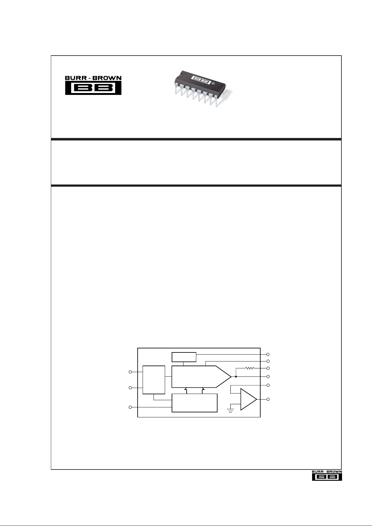
PCM61P
Serial Input 18-Bit Monolithic Audio
DIGITAL-TO-ANALOG CONVERTER
DESCRIPTION
The PCM61P is an 18-bit totally pin compatible performance replacement for the popular 16-bit PCM56P.
With the addition of two extra bits, lower max THD+N
(–92dB; PCM61P-K) can be achieved in audio applications already using the PCM56P. The PCM61P is
complete with internal reference and output op amp and
requires no external parts to function as an 18-bit DAC.
The PCM61P is capable of an 8-times oversampling
rate (single channel) and meets all of its specifications
without an external output deglitcher.
The PCM61P comes in a small, reliable 16-pin plastic
DIP package that has passed operating life tests under
simultaneous high temperature, high humidity and high
pressure testing.
FEATURES
● 18-BIT MONOLITHIC AUDIO D/A
CONVERTER
● LOW MAX THD + N: –92dB Without
External Adjust
● 100% PIN COMPATIBLE WITH INDUSTRY
STD 16-BIT PCM56P
● LOW GLITCH OUTPUT OF
±3V OR ±1mA
● CAPABLE OF 8X OVERSAMPLING RATE
IN V
OUT
MODE
● COMPLETE WITH INTERNAL REFERENCE
AND OUTPUT OP AMP
● RELIABLE PLASTIC 16-PIN DIP PACKAGE
MSB Adj
Ref
R
Serial-To-Parallel
Shift Register
18-Bit
DAC
Control
Logic
VREF
Clock
Data
Latch Enable
F
+
_
SJ
OUT
I
OUT
I
OUT
V
®
International Airport Industrial Park • Mailing Address: PO Box 11400, Tucson, AZ 85734 • Street Address: 6730 S. Tucson Blvd., Tucson, AZ 85706 • Tel: (520) 746-1111 • Twx: 910-952-1111
Internet: http://www.burr-brown.com/ • FAXLine: (800) 548-6133 (US/Canada Only) • Cable: BBRCORP • Telex: 066-6491 • FAX: (520) 889-1510 • Immediate Product Info: (800) 548-6132
PCM61P
®
PCM61P
2
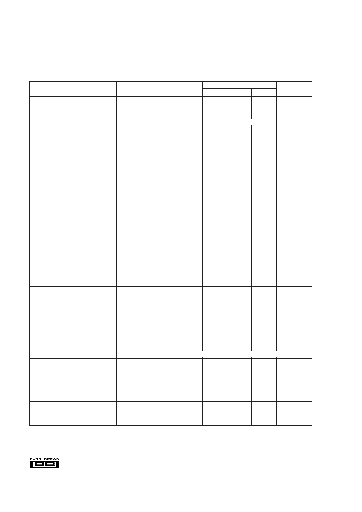
SPECIFICATIONS
ELECTRICAL
All specifications at 25°C, and +VCC = +5V, unless otherwise noted.
NOTES: (1) Binary Two’s Complement coding. (2) Ratio of (Distortion
RMS
+ Noise
RMS
)/Signal
RMS
. (3) D/A converter output frequency/signal level. (4) D/A converter
sample frequency (4 x 44.1kHz; 4 times oversampling). (5) Bipolar zero, using A-weighted filter. (6) This is the combined drift error due to gain, offset, and linearity over
temperature. (7) All positive and all negative supply pins must be tied together respectively.
PCM61P-P, J-P, K
PARAMETER CONDITIONS MIN TYP MAX UNITS
RESOLUTION 18 Bits
DYNAMIC RANGE 108 dB
DIGITAL INPUT
Logic Family TTL/CMOS Compatible
Logic Level: V
IH
+2.4 +V
L
V
V
IL
0 +0.8 V
I
IH
VIH = +2.7V +1 µA
I
IL
VIL = +0.4V –50 µA
Data Format Serial BTC
(1)
Input Clock Frequency 16.9 MHz
DYNAMIC CHARACTERISTICS
Total Harmonic Distortion + N
(2)
Without MSB Adjustments
PCM61P
f = 991Hz (0dB)
(3)
fS = 176.4kHz
(4)
–88 –82 dB
f = 991Hz (–20dB) f
S
= 176.4kHz –74 –68 dB
f = 991Hz (–60dB) f
S
= 176.4kHz –34 –28 dB
PCM61P-J
f = 991Hz (0dB) f
S
= 176.4kHz –94 –88 dB
f = 991Hz (–20dB) f
S
= 176.4kHz –76 –74 dB
f = 991Hz (–60dB) f
S
= 176.4kHz –36 –34 dB
PCM61P-K
f = 991Hz (0dB) f
S
= 176.4kHz –98 –92 dB
f = 991Hz (–20dB) f
S
= 176.4kHz –80 –74 dB
f = 991Hz (–60dB) f
S
= 176.4kHz –40 –34 dB
IDLE CHANNEL SNR 20Hz to 20kHz at BPZ
(5)
112 dB
TRANSFER CHARACTERISTICS
ACCURACY
Gain Error ±2 %FSR
Bipolar Zero Error ±30 mV
Differential Linearity Error ±0.001 %FSR
Total Drift
(6)
0°C to 70°C ±25 ppm of FSR/°C
Bipolar Zero Drift 0°C to 70°C ±4 ppm of FSR/°C
Warm-up Time 1 Minute
MONOTONICITY 16 Bits
ANALOG OUTPUT
Voltage: Output Range ±3V
Output Current ±2mA
Output Impedance 0.1 Ω
Current: Output Range ±30% ±1mA
Output Impedance ±30% 1.2 kΩ
SETTLING TIME To ±0.006% of FSR
Voltage: 6V Step 1.5 µs
1 LSB 1.0 µs
Slew Rate 12 V/µs
Current: 1mA Step 10Ω to 100Ω Load 250 ns
1mA Step 1kΩ Load 350 ns
Glitch Energy Meets all THD+N specs without external deglitching
POWER SUPPLY REQUIREMENTS
(7)
±VCC Supply Voltage ±4.75 ±5 ±13.2 V
Supply Current: +I
CC
+VCC = +5V +10 +17 mA
+I
CC
+VCC = +12V +12 mA
–I
CC
–VCC = –5V –25 –35 mA
–I
CC
–VCC = –12V –27 mA
Power Dissipation ±V
CC
= ±5V 175 260 mW
±V
CC
= ±12V 475 mW
TEMPERATURE RANGE
Specification 0 +70 °C
Operating –30 +70 °C
Storage –60 +100 °C
 Loading...