

Burr Brown PCM56P-L, PCM56U, PCM56U-1K, PCM56P, PCM56P-J Datasheet
...
FEATURES
● SERIAL INPUT
● –92dB MAX THD: FS Input, K Grade
● –74dB MAX THD: –20dB Input, K Grade
● 96dB DYNAMIC RANGE
● NO EXTERNAL COMPONENTS REQUIRED
● 16-BIT RESOLUTION
● 15-BIT MONOTONICITY, TYP
● 0.001% OF FSR TYP DIFFERENTIAL
LINEARITY ERROR
● 1.5
µs SETTLING TIME, TYP: Voltage Out
●
±3V OR ±1mA AUDIO OUTPUT
● EIAJ STC-007-COMPATIBLE
● OPERATES ON
±5V TO ±12V SUPPLIES
● PINOUT ALLOWS I
OUT
OPTION
● PLASTIC DIP OR SOIC PACKAGE
This converter is completely self-contained with a
stable, low noise, internal zener voltage reference;
high speed current switches; a resistor ladder network; and a fast settling, low noise output operational
amplifier all on a single monolithic chip. The
converters are operated using two power supplies that
can range from ±5V to ±12V. Power dissipation with
±5V supplies is typically less than 200mW. Also
included is a provision for external adjustment of the
MSB error (differential linearity error at bipolar zero)
to further improve total harmonic distortion (THD)
specifications if desired. Few external components
are necessary for operation, and all critical
specifications are 100% tested. This helps assure the
user of high system reliability and outstanding overall
system performance.
The PCM56 is packaged in a high-quality 16-pin
molded plastic DIP package or SOIC and has passed
operating life tests under simultaneous high-pressure,
high-temperature, and high-humidity conditions.
DESIGNED FOR AUDIO
PCM56P
PCM56U
®
International Airport Industrial Park • Mailing Address: PO Box 11400 • Tucson, AZ 85734 • Street Address: 6730 S. Tucson Blvd. • Tucson, AZ 85706
Tel: (520) 746-1111 • Twx: 910-952-1111 • Cable: BBRCORP • Telex: 066-6491 • FAX: (520) 889-1510 • Immediate Product Info: (800) 548-6132
DESCRIPTION
The PCM56 is a state-of-the-art, fully monotonic,
digital-to-analog converter that is designed and
specified for digital audio applications. This device
employs ultra-stable nichrome (NiCr) thin-film
resistors to provide monotonicity, low distortion, and
low differential linearity error (especially around
bipolar zero) over long periods of time and over the
full operating temperature.
RF
Audio
Output
Reference
16-Bit
I
OUT
DAC
16-Bit Input Latch
16-Bit Serial-to-Parallel Conversion
Clock LE Data
Serial Input 16-Bit Monolithic
DIGITAL-TO-ANALOG CONVERTER
©
1987 Burr-Brown Corporation PDS-700D Printed in U.S.A. August, 1993
2
®
PCM56
DIGITAL INPUT
Resolution 16 Bits
Digital Inputs
(1)
: V
IH
+2.4 +V
L
V
V
IL
0 +0.8 V
I
IH
, VIN = +2.7V +1.0 µA
I
IL
, VIN = +0.4V –50 µA
Input Clock Frequency 10.0 MHz
TRANSFER CHARACTERISTICS
ACCURACY
Gain Error ±2.0 %
Bipolar Zero Error ±30 mV
Differential Linearity Error ±0.001 % of FSR
(2)
Noise (rms, 20Hz to 20kHz) at Bipolar Zero (V
OUT
models) 6 µV
TOTAL HARMONIC DISTORTION
V
O
= ±FS at f = 991Hz: PCM56P-K –94 –92 dB
PCM56P-J –94 –88 dB
PCM56P, PCM56U –94 –82 dB
PCM56P-L –94 –80 dB
V
O
= –20dB at f = 991Hz: PCM56P-K –75 –74 dB
PCM56P-J –75 –68 dB
PCM56P, PCM56U –75 –68 dB
PCM56P-L –75 –60 dB
V
O
= –60dB at f = 991Hz: PCM56P-K –35 –34 dB
PCM56P-J –35 –28 dB
PCM56P, PCM56U –35 –28 dB
PCM56P-L –35 –20 dB
MONOTONICITY 15 Bits
DRIFT (0°C to +70°C)
Total Drift
(3)
±25 ppm of FSR/°C
Bipolar Zero Drift ±4 ppm of FSR/°C
SETTLING TIME (to ±0.006% of FSR)
Voltage Output: 6V Step 1.5 µs
1LSB 1.0 µs
Slew Rate 10 V/µs
Current Output, 1mA Step: 10Ω to 100Ω Load 350 ns
1kΩ Load
(4)
350 ns
WARM-UP TIME 1Min
OUTPUT
Voltage Output Configuration: Bipolar Range ±3.0 V
Output Current ±2.0 mA
Output Impedance 0.10 Ω
Short Circuit Duration
Current Output Configuration:
Bipolar Range (±30%) ±1.0 mA
Output Impedance (±30%) 1.2 kΩ
POWER SUPPLY REQUIREMENTS
(5)
Voltage: +VS and +V
L
+4.75 +5.00 +13.2 V
–V
S
and –V
L
–4.75 –5.00 –13.2 V
Supply Drain (No Load): +V (+V
S
and +VL = +5V) +10.00 +17.0 mA
–V (–V
S
and –VL = –5V) –25.0 –35.0 mA
+V (+V
S
and +VL = +12V) +12.0 mA
–V (–V
S
and –VL = –12V) –27.0 mA
Power Dissipation: V
S
and VL = ±5V 175 260 mW
V
S
and VL = ±12V 468 mW
TEMPERATURE RANGE
Specification 0 +70 °C
Operation –25 +70 °C
Storage –60 +100 °C
NOTES: (1) Logic input levels are TTL/CMOS-compatible. (2) FSR means full-scale range and is equivalent to 6V (±3V) for PCM56 in the V
OUT
mode. (3) This is the
combined drift error due to gain, offset, and linearity over temperature. (4) Measured with an active clamp to provide a low impedance for approximately 200ns. (5) All
specifications assume +V
S
connected to +VL and –VS connected to –VL. If supplies are connected separately, –VL must not be more negative than –VS supply voltage
to assure proper operation. No similar restriction applies to the value of +V
L
with respect to +VS.
PCM56U, PCM56P-J, -K
PARAMETER MIN TYP MAX UNITS
SPECIFICATIONS
ELECTRICAL
Typical at +25°C, and nominal power supply voltages ±5V, unless otherwise noted.
Indefinite to Common
3
®
PCM56
DC Supply Voltages ......................................................................±16VDC
Input Logic Voltage ............................................................–1V to +V
S
/+V
L
Power Dissipation .......................................................................... 850mW
Operating Temperature..................................................... –25°C to +70°C
Storage Temperature ...................................................... –60°C to +100°C
Lead Temperature (soldering, 10s)................................................ +300°C
ABSOLUTE MAXIMUM RATINGS
PACKAGE INFORMATION
PACKAGE DRAWING
MODEL PACKAGE NUMBER
(1)
PCM56U 16-Pin SOIC 211
PCM56P 16-Pin Plastic DIP 180
PCM56P-J 16-Pin Plastic DIP 180
PCM56P-K 16-Pin Plastic DIP 180
PCM56P-L 16-Pin Plastic DIP 180
NOTE: (1) For detailed drawing and dimension table, please see end of data
sheet, or Appendix D of Burr-Brown IC Data Book.
PIN DESCRIPTION MNEMONIC
P1 Analog Negative Supply –V
S
P2 Logic Common LOG COM
P3 Logic Positive Supply +V
L
P4 No Connection NC
P5 Clock Input CLK
P6 Latch Enable Input LE
P7 Serial Data Input DATA
P8 Logic Negative Supply –V
L
P9 Voltage Output V
OUT
P10 Feedback Resistor RF
P11 Summing Junction SJ
P12 Analog Common ANA COM
P13 Current Output I
OUT
P14 MSB Adjustment Terminal MSB ADJ
P15 MSB Trim-pot Terminal TRIM
P16 Analog Positive Supply +V
S
PIN ASSIGNMENTS
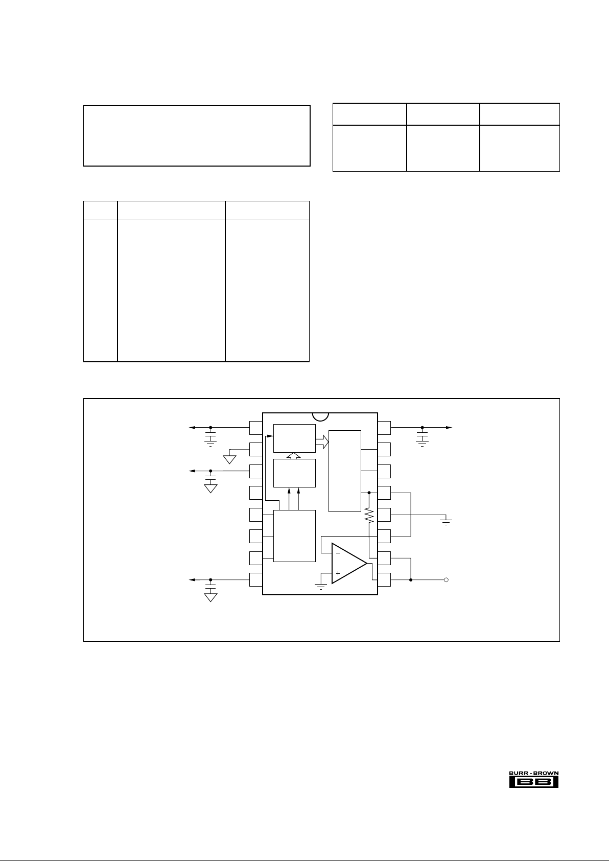
CONNECTION DIAGRAM
16-Bit
DAC Latch
16-Bit Serial
to Parallel
Conversion
Control
Logic and
Level
Shifting
Circuit
1
2
3
4
5
6
7
8
16
15
14
13
12
11
10
9
16-Bit
I
OUT
DAC
–5V
+5V
–5V
1µF
1µF
1µF
Logic
Common
–V
S
+V
L
NC
CLK
LE
Data
–V
L
–V
S
Analog
Common
SJ
RF
V
OUT
(±3.0V)
Trim
(1)
MSB Adjust
(1)
I
OUT
Analog
Output
1µF
+5V
NOTE: (1) MSB error (Bipolar Zero differential linearity error)
can be adjusted to zero using the external circuit shown in Figure 6.
 Loading...