

Burr Brown PCM54HP, PCM54JP, PCM54KP, PCM55HP, PCM55HP-1K Datasheet
...
PCM54
PCM55
FEATURES
● PARALLEL INPUT FORMAT
● 16-BIT RESOLUTION
● 15-BIT MONOTONICITY (typ)
● –92dB TOTAL HARMONIC DISTORTION
(K Grade)
● 3µs SETTLING TIME (Voltage Out)
● 96dB DYNAMIC RANGE
● ±3V or ±1mA AUDIO OUTPUT
● OPERATES ON ±5V (PCM55) TO ±12V
(PCM54) SUPPLIES
● 28-PIN DIP (PCM54)
● 24-LEAD SOIC (PCM55)
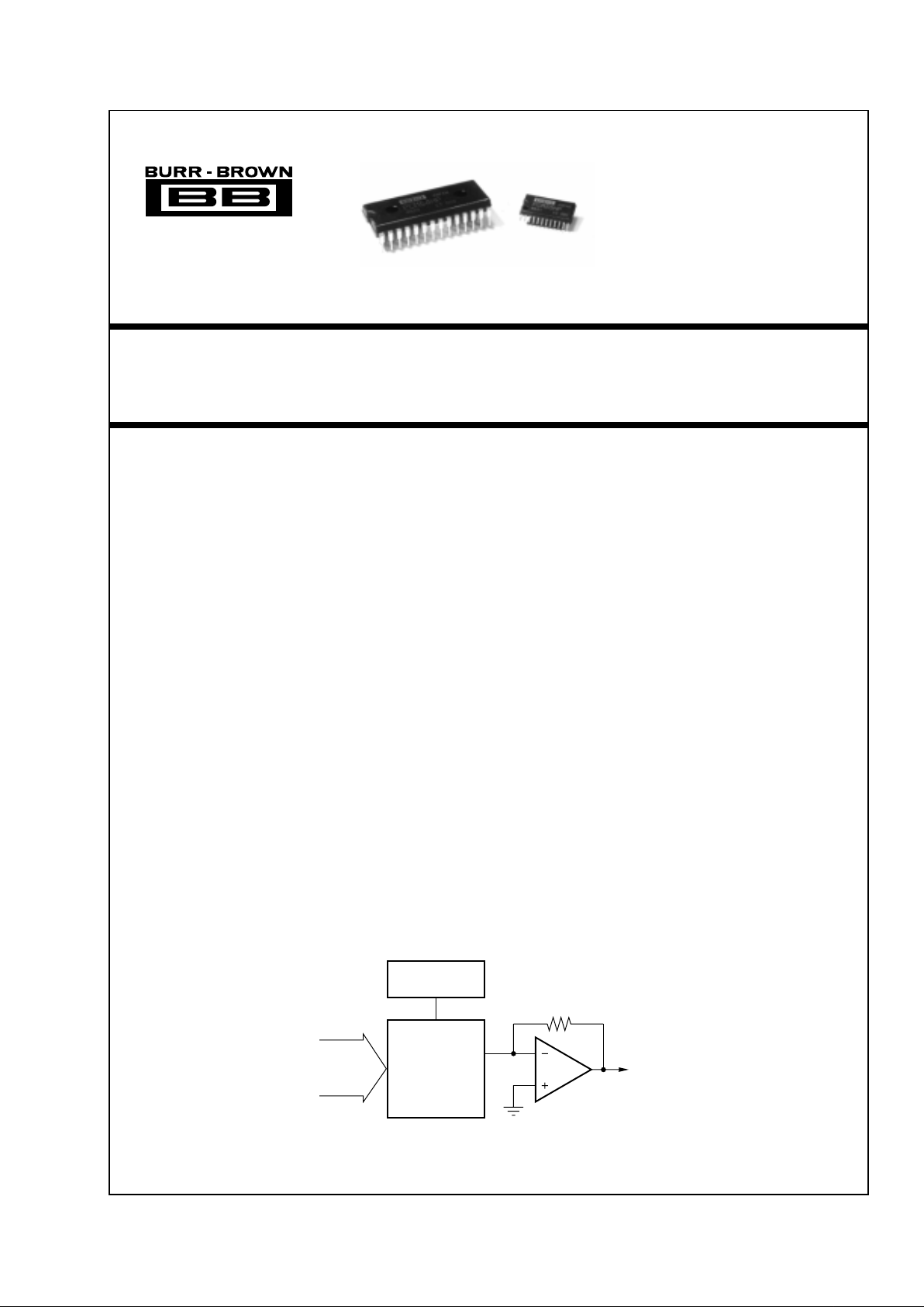
16-Bit Monolithic
DIGITAL-TO-ANALOG CONVERTERS
DESIGNED FOR AUDIO
DESCRIPTION
The PCM54 and PCM55 family of converters are
parallel input, fully monotonic, 16-bit digital-to-analog converters that are designed and specified for
digital audio applications. These devices employ ultra-stable nichrome (NiCr) thin-film resistors to provide monotonicity, low distortion, and low differential
linearity error (especially around bipolar zero) over
long periods of time and over the full operating
temperature.
These converters are completely self-contained with a
stable, low noise, internal, zener voltage reference;
high speed current switches; a resistor ladder
network; and a fast settling, low noise output operational amplifier all on a single monolithic chip. The
converters are operated using two power supplies that
can range from ±5V (PCM55) to ±12V (PCM54).
Power dissipation with ±5V supplies is typically less
than 200mW. Also included is a provision for external adjustment of the MSB error (differential linearity
error at bipolar zero, PCM54 only) to further improve
Total Harmonic Distortion (THD) specifications if
desired.
A current output (I
OUT
) wiring option is provided. This
output typically settles to within ±0.006% of FSR
final value in 350ns (in response to a full-scale change
in the digital input code).
The PCM54 is packaged in 28-pin plastic DIP package. The PCM55 is available in a 24-lead plastic miniflatpak.
16-Bit Ladder
Resistor Network
and
Current Switches
Reference
Voltage
Parallel
Digital
Input
R
F
Output
Operational
Amplifier
Audio Output
(Voltage)
®
International Airport Industrial Park • Mailing Address: PO Box 11400, Tucson, AZ 85734 • Street Address: 6730 S. Tucson Blvd., Tucson, AZ 85706 • Tel: (520) 746-1111 • Twx: 910-952-1111
Internet: http://www.burr-brown.com/ • FAXLine: (800) 548-6133 (US/Canada Only) • Cable: BBRCORP • Telex: 066-6491 • FAX: (520) 889-1510 • Immediate Product Info: (800) 548-6132
©
1985 Burr-Brown Corporation PDS-619B Printed in U.S.A. August, 1998
®
PCM54/55
2
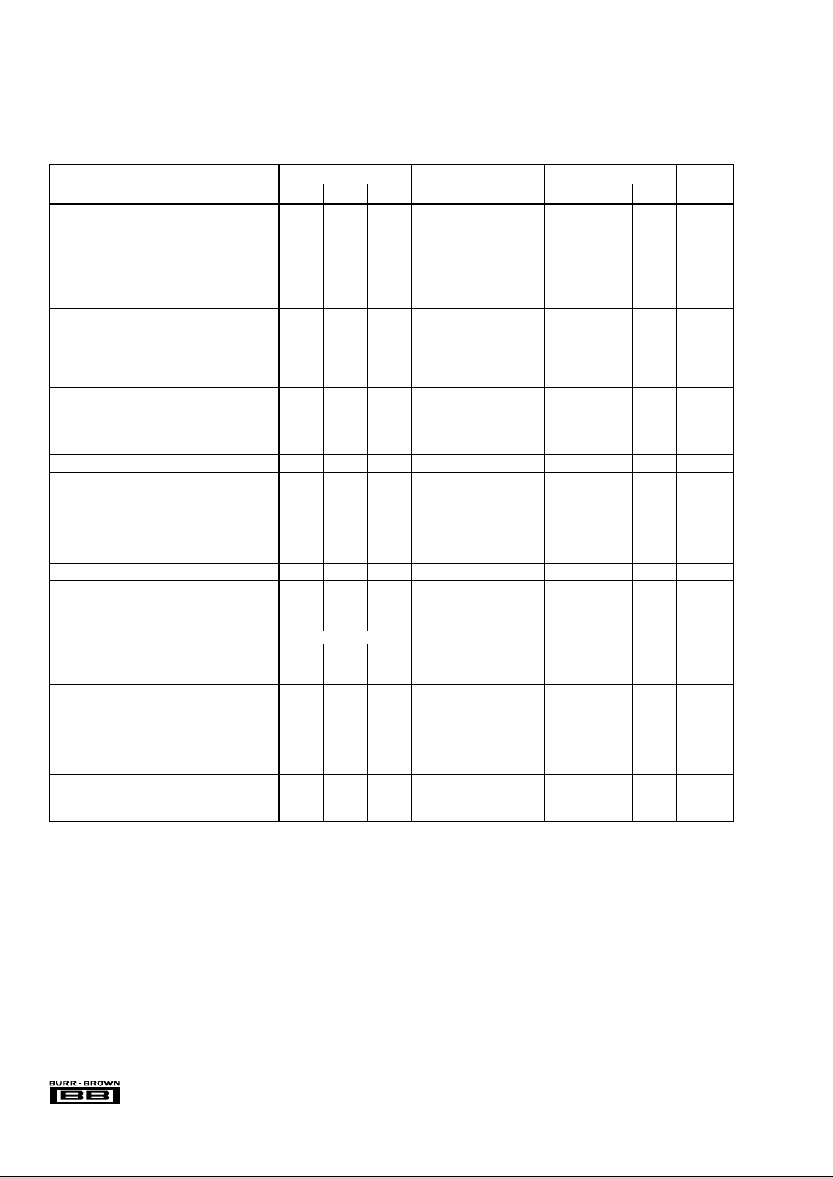
SPECIFICATIONS
ELECTRICAL
At +25°C and ±VCC = 12V, unless otherwise noted.
✽ Specifications same as for PCM54HP.
NOTES: (1) Externally adjustable. If external adjustment is not used, connect a 0.01µF capacitor to Common to reduce noise pickup. (2) FSR means Full-Scale Range
and is 6V for ±3V output. (3) The measurement of total harmonic distortion is highly dependent on the characteristics of the measurement circuit. Burr-Brown may
calculate THD from the measured linearity errors using Equation 2 in the section on “Total Harmonic Distortion,” but specifies that the maximum THD measured with
the circuit shown in Figure 2 will be less than the limits indicated. (4) Measured with an active clamp to provide a low impedance for approximately 200ns. (5) Deglitcher
or sample/hold delay used in THD measurement test circuit. See Figures 2 and 3. (6) Output amplifier disconnected.
PCM54HP, PCM55HP PCM54JP, PCM55JP PCM54KP
PARAMETER MIN TYP MAX MIN TYP MAX MIN TYP MAX UNITS
DIGITAL INPUTS
Resolution 16 ✽✽Bits
Dynamic Range 96 ✽✽dB
Logic Levels (TTL/CMOS Compatible):
V
IH
+2.4 +5.25 ✽✽✽✽V
V
IL
0 +0.8 ✽✽✽✽V
I
IH
, VIN = +2.7V +40 ✽✽µA
I
IL
, VIN = +0.4V –0.5 ✽✽mA
TRANSFER CHARACTERISTICS
ACCURACY
Gain Error ±2 ✽✽%
Bipolar Zero Error ±30 ✽✽mV
Differential Linearity Error at Biploar Zero
(1)
±0.001 ✽✽% FSR
(2)
Noise (rms) (20Hz to 20kHz) at Bipolar Zero 12 ✽✽µV
TOTAL HARMONIC DISTORTION
(3)
(16-Bit Resolution)
V
O
= ±FS at f = 991Hz –94 –82 ✽ –88 ✽✽–92 dB
V
O
= –20dB at f = 991Hz –74 –68 ✽✽✽–80 –74 dB
V
O
= –60dB at f = 991Hz –34 –28 ✽✽✽–40 –34 dB
MONOTONICITY 15 ✽✽Bits
SETTLING TIME (to ±0.006% of FSR)
Voltage Output: 6V Step 3 ✽✽µs
1LSB Step 1 ✽✽µs
Current Output (1mA Step):10Ω to 100Ω Load 350 ✽✽ns
1kΩ Load
(4)
350 ✽✽ns
Deglitcher Delay (THD Test)
(5)
2.5 4 ✽✽ ✽✽ µs
Slew Rate 10 ✽✽V/µs
WARM-UP TIME 1 ✽✽Min
ANALOG OUTPUT
Voltage Output: Bipolar Range ±3 ✽✽V
Output Current ±2 ✽✽mA
Output Impedance 0.1 ✽✽Ω
Short-Circuit Duration Indefinite to Common ✽✽
Current Output:
(6)
Bipolar Range (±30%) ±1 ✽✽mA
Bipolar Output Impedance (±30%) 1.2 ✽✽kΩ
POWER SUPPLY REQUIREMENTS
Voltage: +V
CC
(PCM54) +4.75 +12 +15.75 ✽✽✽✽✽✽ V
–V
CC
(PCM54) –4.75 –12 –15.75 ✽✽✽✽✽✽ V
+V
CC
(PCM55) +4.75 +5 +7.5 ✽✽✽✽✽✽ V
–V
CC
(PCM55) –4.75 –5 –7.5 ✽✽✽✽✽✽ V
Supply Drain: +V
CC
+13 +20 ✽✽ ✽✽mA
–V
CC
–16 –25 ✽✽ ✽✽mA
TEMPERATURE RANGE
Operating 0 +70 ✽✽✽✽°C
Storage –55 +100 ✽✽✽✽°C
The information provided herein is believed to be reliable; however, BURR-BROWN assumes no responsibility for inaccuracies or omissions. BURR-BROWN
assumes no responsibility for the use of this information, and all use of such information shall be entirely at the user’s own risk. Prices and specifications are subject
to change without notice. No patent rights or licenses to any of the circuits described herein are implied or granted to any third party. BURR-BROWN does not
authorize or warrant any BURR-BROWN product for use in life support devices and/or systems.
®
PCM54/55
3
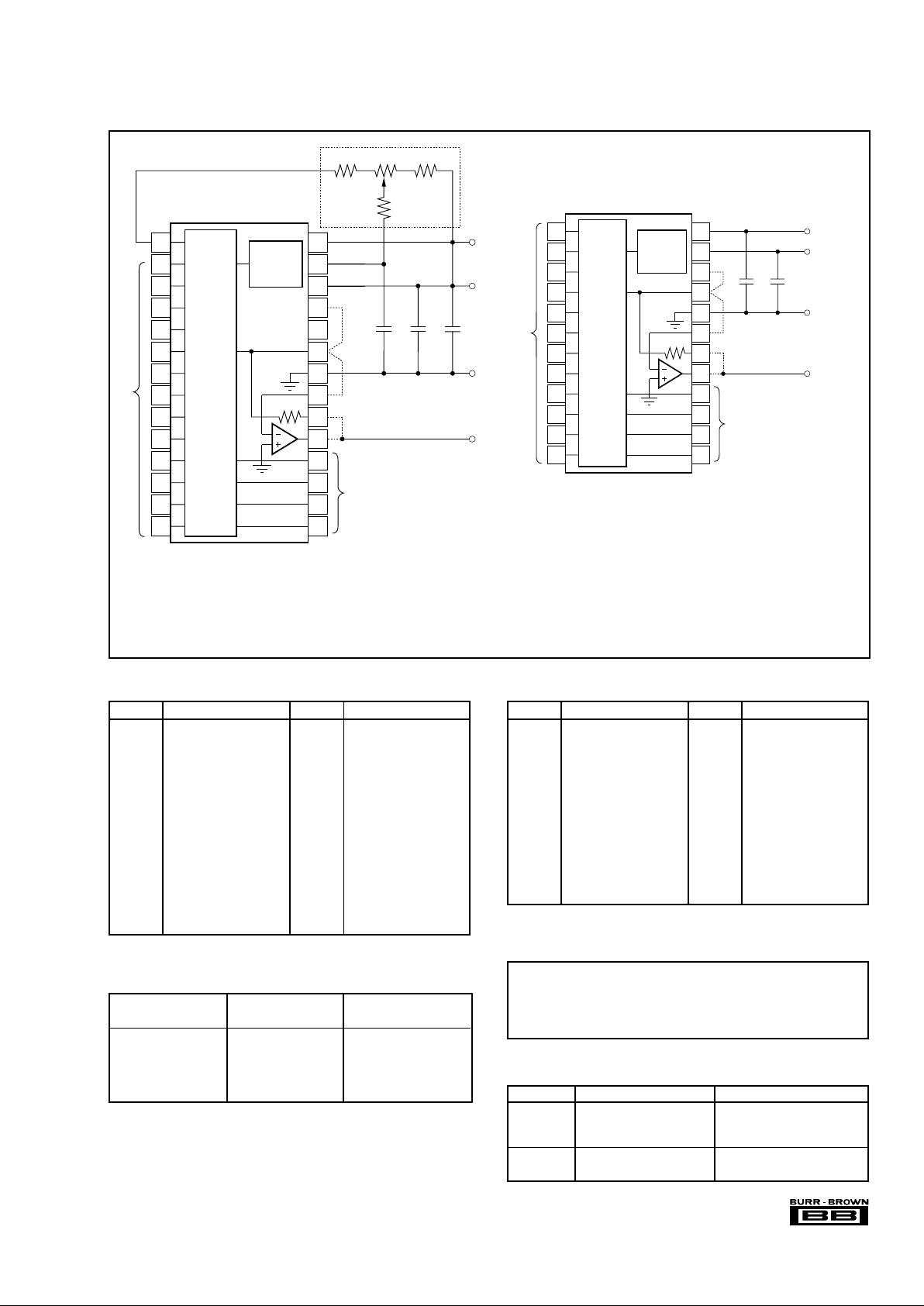
CONNECTION DIAGRAMS
PIN PCM54-DIP PIN PCM54-DIP
1 Trim 15 Bit 13
2 Bit 1 (MSB) 16 Bit 14
3 Bit 2 17 Bit 15
4 NC 18 Bit 16 (LSB)
5 Bit 3 19 V
OUT
6 Bit 4 20 R
FB
7 Bit 5 21 SJ
8 Bit 6 22 Common
9 Bit 7 23 I
OUT
10 Bit 8 24 NC
11 Bit 9 25 I
BPO
12 Bit 10 26 +V
CC
13 Bit 11 27 MSB Adjust
14 Bit 12 28 –V
CC
PIN ASSIGNMENTS
PIN PCM55-SOIC PIN PCM55-SOIC
1 Bit 1 (MSB) 13 Bit 13
2 Bit 2 14 Bit 14
3 Bit 3 15 Bit 15
4 Bit 4 16 Bit 16
5 Bit 5 17 V
OUT
6 Bit 6 18 Feedback Resistor
7 Bit 7 19 Summing Junction
8 Bit 8 20 Common
9 Bit 9 21 Current Output
10 Bit 10 22 Bipolar Offset
11 Bit 11 23 +V
CC
12 Bit 12 24 –V
CC
PIN ASSIGNMENTS
DC Supply Voltage ...................................................................... ±18VDC
Input Logic Voltage ............................................................... –1V to +5.5V
Power Dissipation ..................................PCM54 800mW, PCM55 400mW
Storage Temperature...................................................... –55°C to +100°C
Lead Temperature, (soldering, 10s) .............................................. +300°C
ABSOLUTE MAXIMUM RATINGS
ORDERING INFORMATION
PACKAGE INFORMATION
PACKAGE DRAWING
PRODUCT PACKAGE NUMBER
(1)
PCM54HP 28-Pin DIP 215
PCM54JP 28-Pin DIP 215
PCM54KP 28-Pin DIP 215
PCM55HP 24-Lead SOIC 178
PCM55JP 24-Lead SOIC 178
NOTE: (1) For detailed drawing and dimension table, please see end of data
sheet, or Appendix C of Burr-Brown IC Data Book.
PRODUCT THD at FS PACKAGE
PCM54HP 0.008 28-Pin DIP
PCM54JP 0.004 28-Pin DIP
PCM54KP 0.0025 28-Pin DIP
PCM55HP 0.008 24-Lead SOIC
PCM55JP 0.004 24-Lead SOIC
1
2
3
4
5
6
7
8
9
10
11
12
13
14
28
27
26
25
24
23
22
21
20
19
18
17
16
15
0.1µF
PCM54
16-Bit
Ladder
Resistor
Network
and
Switches
Zener
Voltage
Reference
Data
Inputs
1µF
1µF
(2)
(3)
+
+
Common
+V
CC
Audio
V
OUT
100kΩ
560kΩ 330kΩ
1MΩ
(1)
–V
CC
(Optional)
Data Inputs
24
23
22
21
20
19
18
17
16
15
14
13
1µF
PCM55
16-Bit
Ladder
Resistor
Network
and
Switches
Zener
Voltage
Reference
Data
Inputs
1µF
(2)
+
Common
+V
CC
Audio
V
OUT
(1)
–V
CC
Data Inputs
1
2
3
4
5
6
7
8
9
10
11
12
+
(2)
NOTES: (1) MSB error (BPZ differential linearity error) can be adjusted to zero
using this external circuit. (2) Connect to bipolar operation (+V
CC
≥ 8.5V for
unipolar operation). (3) Connect for V
OUT
operation. When V
OUT
amp is not being
used (I
OUT
mode), terminate with an external 3kΩ feedback resistor between pin
19 and pin 21, and a 1kΩ resistor between pin 21 and pin 22 to reduce possible
noise effects.
NOTES: (1) Connect for bipolar operation. (+V
CC
≥ 8.5V for unipolar operation.)
(2) Connect for V
OUT
operation. When V
OUT
amp is not being used (I
OUT
mode),
terminate with an external 3kΩ feedback resistor between pin 17 and pin 19, and
a 1kΩ resistor between pin 19 and pin 20 to reduce possible noise effects.
 Loading...