

Burr Brown PCM3501E, PCM3501E-2K Datasheet
®
1 PCM3501
FEATURES
● 16-BIT DELTA-SIGMA DAC AND ADC
● DIFFERENTIAL INPUT AND OUTPUT
● DESIGNED FOR MODEM ANALOG FRONT END:
Supports up to 56kbps Operation
● ANALOG PERFORMANCE:
Sampling Frequency: 7.2kHz to 26kHz
Dynamic Range: 88dB (typ) at fS = 8kHz, fIN = 1kHz
● SYSTEM CLOCK: 512f
S
● MASTER OR SLAVE OPERATION
● ON-CHIP CRYSTAL OSCILLATOR CIRCUIT
● ADC-TO-DAC LOOP-BACK MODE
● TIME SLOT MODE SUPPORTS UP TO
FOUR CODECs ON A SINGLE SERIAL
INTERFACE
DESCRIPTION
The PCM3501 is a low cost, 16-bit CODEC designed
for modem Analog Front End (AFE) and speech processing applications. The PCM3500’s low power operation from +2.7V to +3.6V power supplies, along
with an integrated power-down mode, make it ideal for
portable applications.
The PCM3501 integrates all of the functions needed for
a modem or voice CODEC, including delta-sigma
© 1999 Burr-Brown Corporation PDS-1569A Printed in U.S.A. December, 1999
PCM3501
®
Low Voltage, Low Power, 16-Bit, Mono
VOICE/MODEM CODEC
APPLICATIONS
● SOFTWARE MODEMS FOR:
Personal Digital Assistant
Notebook and Hand-Held PCs
Set-Top Box
Digital Television
Embedded Systems
● PORTABLE VOICE RECORDER/PLAYER
● SPEECH RECOGNITION/SYNTHESIS
● TELECONFERENCING PRODUCTS
TM
digital-to-analog and analog-to-digital converters, input anti-aliasing filter, digital high-pass filter for DC
blocking, and an output low-pass filter. The synchronous serial interface provides for a simple, or glue-free
interface to popular DSP and RISC processors. The
serial interface also supports Time Division Multiplexing (TDM), allowing up to four CODECs to share a
single 4-wire serial bus.
International Airport Industrial Park • Mailing Address: PO Box 11400, Tucson, AZ 85734 • Street Address: 6730 S. Tucson Blvd., Tucson, AZ 85706 • Tel: (520) 746-1111
Twx: 910-952-1111 • Internet: http://www.burr-brown.com/ • Cable: BBRCORP • Telex: 066-6491 • FAX: (520) 889-1510 • Immediate Product Info: (800) 548-6132
● POWER-DOWN MODE: 60µA (typ)
● SINGLE +2.7V TO +3.6V POWER SUPPLY
● SMALL PACKAGE: 24-Lead SSOP
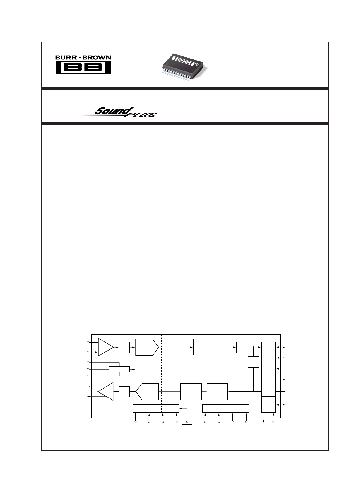
PCM3501
Interpolation
Digital Filter
Mode Control
Decimation
Digital Filter
Reference
AAF HPF
M/S
HPFD TSC
XTIXTOLOOP
V
REF
1
V
COM
V
REF
2
V
IN+
V
IN–
Serial I/O Interface
PDWN
Power
DGND
AGND V
DD
V
CC
Loop
FS
BCK
DIN
DOUT
FSO
SCKIO
Clock
Gen/
OSC
∆Σ
Modulator
(ADC)
∆Σ
Modulator
SMF
V
OUT+
V
OUT–
Multi-Level
DAC

®
2
PCM3501
SPECIFICATIONS
All specifications at TA = +25°C, VDD = V
CC
= 3.3V, fS = 8kHz, and nominal system clock (XTI) = 512fS, and differntial input and output mode, unless otherwise noted.
Measurement band is 100Hz to 0.425f
S
.
NOTES: (1) Pins 6, 7, 8, 9, 10, 15, 17, 18, 19, 20 (M/S, TSC, BCK, FS, DIN, SCKIO, XTI, HPFD, LOOP, PDWN). (2) Pins 8, 9, 10, 15, 17 (BCK, FS, DIN, SCKIO,
XTI (Schmitt-Trigger input). (3) Pins 6, 7, 18, 19, 20 (M/S, TSC, HPFD, LOOP, PDWN; (Schmitt-Trigger input with internal pull-down). (4) Pins 8, 9, 11, 12, 15,
16 (BCK, FS, DOUT, FSO, SCKIO, XTO). (5) If V
COM
load impedance (R
COM
) is lower than 100kΩ, the user needs to connect external resistors to AGND and
V
CC
with resistance of R
COM
/10 or lower. (6) fIN = 1kHz, Audio Precision System II, RMS mode with 3.4kHz LPF, 100Hz HPF.
MSB-First, Binary Two’s Complement
PCM3501E
PARAMETER CONDITIONS MIN TYP MAX UNITS
RESOLUTION 16 Bits
DATA FORMAT
Serial Data Interface Format DSP Format
Serial Data Bit Length 16 Bits
Serial Data Format
Sampling Frequency, f
S
ADC and DAC 7.2 8 26 kHz
System Clock Frequency, 512f
S
3.686 4.096 13.312 MHz
DIGITAL INPUT/OUTPUT
Logic Family CMOS
Input Logic Level: V
IH
(1)
0.7 • V
DD
VDC
V
IL
(1)
0.3 • V
DD
VDC
Input Logic Current: I
IN
(2)
±1 µA
I
IN
(3)
100 µA
Output Logic Level: V
OH
(4)
I
OUT
= –1mA V
DD
– 0.3 VDC
V
OL
(4)
I
OUT
= +1mA 0.3 VDC
REFERENCE
Voltage Common: V
COM
VIN = BPZ, V
OUT
= BPZ 0.5V
CC
V
V
COM
Load Impedance: R
COM
(5)
100 kΩ
ADC CHARACTERISTICS
DC ACCURACY
Input Voltage (Differential) V
IN
= VIN+ – VIN– 1.2V
CC
Vp-p
Gain Error ±2 ±5 % of FSR
Offset Error HPF OFF ±2 % of FSR
Input Resistance 50 kΩ
AC ACCURACY
(6)
THD+N fIN = 1kHz, VIN = –0.5dB –85 –80 dB
Dynamic Range 82 88 dB
Signal-to-Noise Ratio 82 88 dB
Crosstalk DAC Channel Idle, 0dB Input 78 82 dB
Passband Ripple HPF ON, 0.0002f
S
to 0.425f
S
±0.05 dB
HPF OFF, 0f
S
to 0.425f
S
±0.05 dB
Roll-Off HPF ON, at 0.00002f
S
–3 dB
HPF ON, at 0.56f
S
–30 dB
Stopband Rejection 0.58f
S
to f
S
–65 dB
Group Delay 18/f
S
4m sec
DAC CHARACTERISTICS
DC ACCURACY
Output Voltage (Differential) V
OUT
= V
OUT
+ – V
OUT
– 1.2 V
CC
Vp-p
Gain Error ±1 ±5 % of FSR
Offset Error ±1 % of FSR
Load Resistance 10 kΩ
AC ACCURACY
(6)
THD+N fIN = 1kHz, V
OUT
= 0dB –90 –82 dB
Dynamic Range 84 92 dB
Signal-to-Noise Ratio 84 94 dB
Crosstalk ADC Channel Idle, –0.5dB Input 84 92 dB
Passband Ripple 0f
S
to 0.425f
S
±0.4 dB
Group Delay 12/f
S
4m sec
POWER SUPPLY REQUIREMENTS
Voltage Range V
CC
, V
DD
2.7 3.3 3.6 VDC
Supply Current in operation mode V
CC
= VDD =3.3V 9 12 mA
Total Supply Current in Power-Down Mode V
CC
= VDD = 3.3V, XTI Stopped 60 µA
Total Power Dissipation V
CC
= VDD = 3.3V 30 40 mW
TEMPERATURE RANGE
Operating –25 +85 °C
Storage –55 +125 °C
Thermal Resistance,
θ
JA
24-pin SSOP 100 °C/W
®
3 PCM3501
The information provided herein is believed to be reliable; however, BURR-BROWN assumes no responsibility for inaccuracies or omissions. BURR-BROWN assumes no
responsibility for the use of this information, and all use of such information shall be entirely at the user’s own risk. Prices and specifications are subject to change without notice.
No patent rights or licenses to any of the circuits described herein are implied or granted to any third party. BURR-BROWN does not authorize or warrant any BURR-BROWN
product for use in life support devices and/or systems.
Supply Voltage, +VDD, +V
CC
(1)
.......................................................... +6.5V
Supply Voltage Differences
(2)
........................................................... ±0.1V
GND Voltage Differences
(3)
....................................................................................... ±0.1V
Digital Input Voltage................................................... –0.3V to V
DD
+ 0.3V
Input Current (any pins except supply) ........................................... ±10mA
Power Dissipation .......................................................................... 300mW
Operating Temperature Range ......................................... –25°C to +85°C
Storage Temperature...................................................... –55°C to +125°C
Junction Temperature ...................................................................... 150°C
Lead Temperature (soldering, 5s).................................................. +260°C
(reflow, 10s) ................................................................................ +235°C
ABSOLUTE MAXIMUM RATINGS
ELECTROSTATIC
DISCHARGE SENSITIVITY
This integrated circuit can be damaged by ESD. Burr-Brown
recommends that all integrated circuits be handled with
appropriate precautions. Failure to observe proper handling
and installation procedures can cause damage.
ESD damage can range from subtle performance degradation to complete device failure. Precision integrated circuits
may be more susceptible to damage because very small
parametric changes could cause the device not to meet its
published specifications.
PACKAGE SPECIFIED
DRAWING TEMPERATURE PACKAGE ORDERING TRANSPORT
PRODUCT PACKAGE NUMBER RANGE MARKING NUMBER
(1)
MEDIA
PCM3501E 24-Lead SSOP 338 –25°C to +85°C PCM3501E PCM3501E Rails
" " " " " PCM3501E/2K Tape and Reel
NOTE: (1) Models with a slash (/) are available only in Tape and Reel in the quantities indicated (e.g., /2K indicates 2000 devices per reel). Ordering 2,000 pieces
of “PCM3501E/2K” will get a single 2000-piece Tape and Reel.
PACKAGE/ORDERING INFORMATION
NOTES: (1) VCC, VDD. (2) Among VCC, VDD. (3) Among AGND, DGND.
®
4
PCM3501
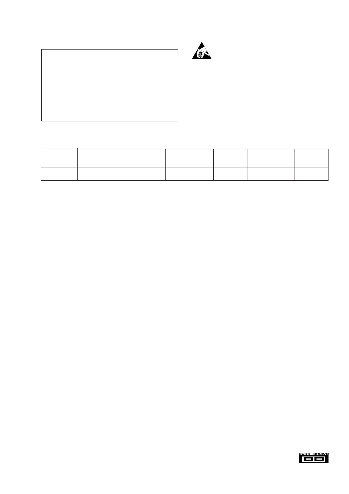
PIN CONFIGURATION
Top View SSOP
PIN NAME I/O DESCRIPTION
1V
COM
OUT Common-Mode Voltage (0.5V
CC)
. This pin should be connected to ground through a capacitor.
2V
REF
1 — Decouple Pin for Reference Voltage 1 (0.99VCC). This pin should be connected to ground through a capacitor.
3V
REF
2 — Decouple Pin for Reference Voltage 2 (0.2VCC). This pin should be connected to ground through a capacitor.
4V
IN+
IN Non-Inverting input to on-chip AFE.
5V
IN–
IN Inverting input to on-chip AFE.
6 M/S IN Master/Slave Select. This pin is used to determine the operating mode for the serial interface. A logic ‘0’ on this pin selects the Slave
Mode. A logic ‘1’ on this pin selects the Master Mode.
(2)
7 TSC IN Time Slot Mode Control. This pin is used to select the time slot operating mode. A logic ‘0’ on this pin disables Time Slot Mode. A
logic ‘1’ on this pin enables Time Slot Mode.
(2)
8 BCK I/O Bit Clock. This pin serves as the bit (or shift) clock for the serial interface. This pin is an input in Slave Mode and an output in Master
Mode.
(1)
9 FS I/O Frame Sync. This pin serves as the frame synchronization clock for the serial interface. This pin is an input in Slave Mode and an
output in Master Mode.
(1)
10 DIN IN Serial Data Input. This pin is used to write 16-bit data to the DAC.
(1)
11 DOUT OUT Serial Data Output. The ADC outputs 16-bit data on this pin.
(3)
12 FSO OUT Frame Sync Output. Active only when Time Slot Mode is enabled. This pin is set to a high impedance state when Time Slot mode
is disabled (TSC = 0).
13 V
DD
— Digital Power Supply. Used to power the digital section of the ADC and DAC, as well as the serial interface and mode control logic.
This pin is not internally connected to V
CC
.
14 DGND — Digital Ground. Internally connected through the substrate to analog ground.
15 SCKIO I/O System Clock Input/Output. This pin is a system clock output when using the crystal oscillator or XTI as the system clock input; when
XTI is connected to ground, this pin is a system clock input.
(1)
16 XTO OUT Crystal Oscillator Output.
17 XTI IN Crystal Oscillator Input or an External System Clock Input.
18 HPFD IN High-Pass Filter Disable. When this pin is set to a logic ‘1’, the HPF function in the ADC is disabled.
(2)
19 LOOP IN ADC-to-DAC Loop-Back Control. When this pin is set to logic ‘1’, the ADC data is fed to the DAC input.
(2)
20 PDWN IN Power Down and Reset Control. When this pin is logic ‘0’, Power-Down Mode is enabled. The PCM3500 is reset on the rising edge
of this signal.
(2)
21 V
OUT–
OUT Inverting output.
22 V
OUT+
OUT Non-inverting output.
23 AGND — Analog Ground. This is the ground for the internal analog circuitry.
24 V
CC
— Analog Power Supply. Used to power the analog circuitry of the ADC and DAC.
NOTES: (1) Schmitt-Trigger input. (2) Schmitt-Trigger input with an internal pull-down resistor. (3) Tri-state output in Time Slot Mode.
PIN ASSIGNMENTS
V
COM
V
REF
1
V
REF
2
V
IN+
V
IN–
M/S
TSC
BCK
FS
DIN
DOUT
FSO
V
CC
AGND
V
OUT+
V
OUT–
PDWN
LOOP
HPFD
XTI
XTO
SCKIO
DGND
V
DD
1
2
3
4
5
6
7
8
9
10
11
12
24
23
22
21
20
19
18
17
16
15
14
13
PCM3501
®
5 PCM3501
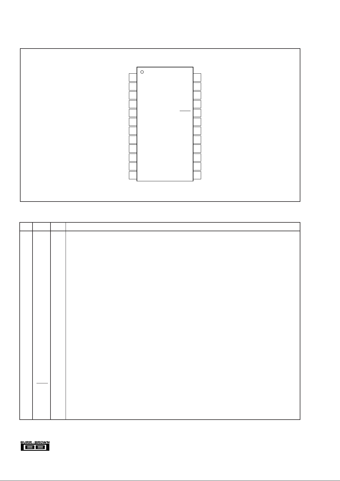
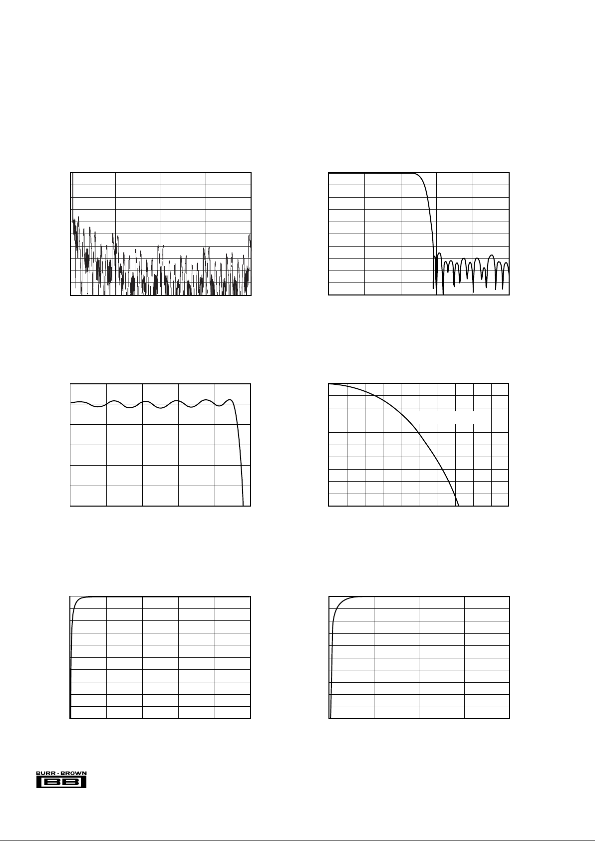
TYPICAL PERFORMANCE CURVES
INTERPOLATION FILTER
PASSBAND RIPPLE CHARACTERISTICS
0.2
0.0
–0.2
–0.4
–0.6
–0.8
–1.0
0 0.1 0.2 0.3 0.4 0.5
Amplitude (dB)
Normalized Frequency (• fS Hz)
OUTPUT FILTER FREQUENCY RESPONSE
STOPBAND CHARACTERISTICS
Frequency (Hz)
Amplitude (dB)
0
–10
–20
–30
–40
–50
–60
–70
–80
–90
–100
100 1k 10k 100k 1M 10M
ANALOG FILTER
DAC SECTION
DIGITAL FILTER
OUTPUT FILTER FREQUENCY RESPONSE
PASSBAND CHARACTERISTICS
Frequency (Hz)
Amplitude (dB)
0
–0.1
–0.2
–0.3
–0.4
–0.5
–0.6
–0.7
–0.8
–0.9
–1.0
100101 1k 10k 100k
Amplitude (dB)
INTERPOLATION FILTER FREQUENCY RESPONSE
Normalized Frequency (• f
S
)
0
–10
–20
–30
–40
–50
–60
–70
–80
–90
–100
0
1
23
4
®
6
PCM3501
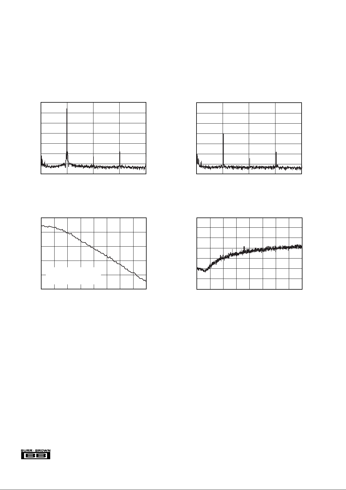
TYPICAL PERFORMANCE CURVES (Cont.)
TA = +25°C, VCC = VDD = +3.3V, fS = 8kHz, and f
SIGNAL
= 1kHz, unless otherwise specified.
DAC OUTPUT SPECTRUM (–0dB, N = 8192)
Frequency (kHz)
Amplitude (dB)
0
–20
–40
–60
–80
–100
–120
–140
12340
DAC OUTPUT SPECTRUM (–60dB, N = 8192)
Frequency (kHz)
Amplitude (dB)
0
–20
–40
–60
–80
–100
–120
–140
12340
DAC OUT-OF-BAND NOISE SPECTRUM
(BPZ, N = 2048)
Frequency (kHz)
Amplitude (dB)
0
–20
–40
–60
–80
–100
–120
–140
8 162432 404856640
DAC SECTION
DAC OUTPUT SPECTRA
TOTAL HARMONIC DISTORTION + NOISE
vs SIGNAL LEVEL
Signal Level (dB)
THD+N (dB)
0
–20
–40
–60
–80
–100
–84 –72 –60 –48 –36 –24 –12 0–96
THD+N fluctuates with signal level
as harmonics are limited to second
and third components.
®
7 PCM3501
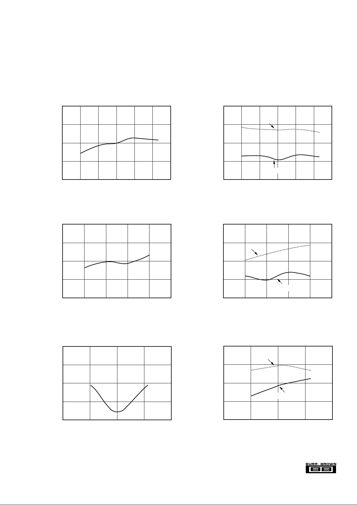
TYPICAL PERFORMANCE CURVES (Cont.)
DAC SECTION
DAC CHARACTERISTICS vs TEMPERATURE, SUPPLY, AND SAMPLING FREQUENCY
THD+N at –0dB (dB)
TOTAL HARMONIC DISTORTION + NOISE
vs TEMPERATURE
(T
A
= –25°C to +85°C)
Temperature (°C)
–88
–90
–92
–94
–96
–25 0 25 50 75 100–50
Dynamic Range and SNR (dB)
DYNAMIC RANGE AND SIGNAL-TO-NOISE RATIO
vs TEMPERATURE
(T
A
= –25°C to +85°C)
Temperature (°C)
100
98
96
94
92
–25 0 25 50 75 100–50
Dynamic Range
SNR
THD+N at –0dB (dB)
TOTAL HARMONIC DISTORTION + NOISE
vs SUPPLY VOLTAGE
(V
CC
= VDD = +2.7V to +3.6V)
Supply Voltage (V)
–88
–90
–92
–94
–96
2.7 3.0 3.3 3.6 3.92.4
THD+N at –0dB (dB)
TOTAL HARMONIC DISTORTION + NOISE
vs SAMPLING FREQUENCY
(f
S
= 8kHz to 26kHz)
f
S
(kHz)
–88
–90
–92
–94
–96
81624320
BW = 3.4kHz
VOUT+
Dynamic Range and SNR (dB)
DYNAMIC RANGE AND SIGNAL-TO-NOISE RATIO
vs SAMPLING FREQUENCY
(f
S
= 8kHz to 26kHz)
f
S
(kHz)
100
98
96
94
92
81624320
BW = 3.4kHz
Dynamic Range
SNR
Dynamic Range and SNR (dB)
DYNAMIC RANGE AND SIGNAL-TO-NOISE RATIO
vs SUPPLY VOLTAGE
(V
CC
= VDD = +2.7V to +3.6V)
Supply Voltage (V)
100
98
96
94
92
2.7 3.0 3.3 3.6 3.92.4
Dynamic Range
SNR
®
8
PCM3501
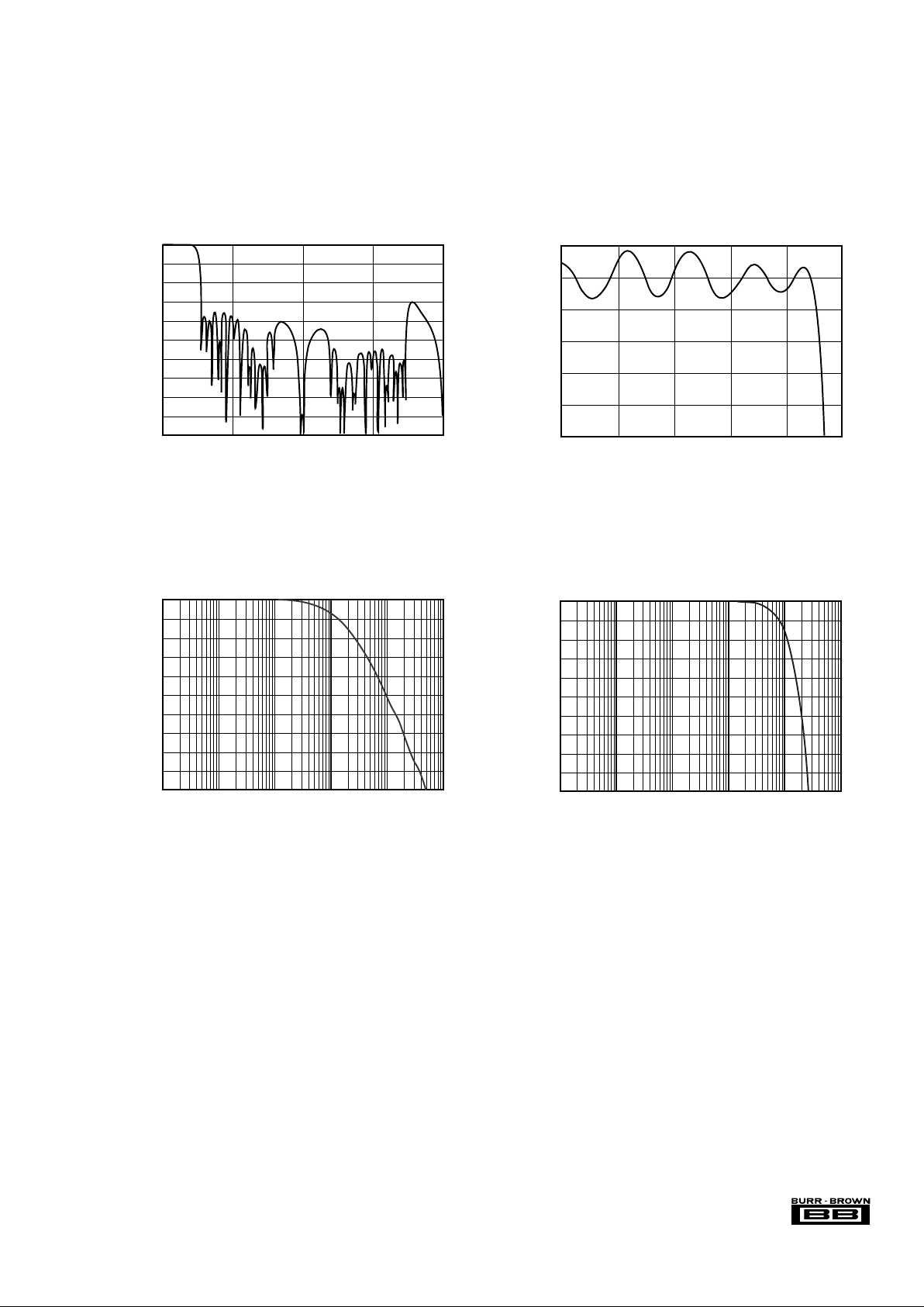
TYPICAL PERFORMANCE CURVES
ADC SECTION
DIGITAL FILTER
DECIMATION FILTER FREQUENCY RESPONSE
Normalized Frequency (• f
S
Hz)
Amplitude (dB)
0
–20
–40
–60
–80
–100
–120
–140
–160
–180
–200
81624320
DECIMATION FILTER
STOPBAND ATTENUATION CHARACTERISTICS
Normalized Frequency (• f
S
Hz)
Amplitude (dB)
0
–10
–20
–30
–40
–50
–60
–70
–80
–90
–100
0.2 0.4 0.6 0.8 1.00
DECIMATION FILTER
PASSBAND RIPPLE CHARACTERISTICS
Normalized Frequency (• f
S
Hz)
Amplitude (dB)
0.2
0.0
–0.2
–0.4
–0.6
–0.8
–1.0
0.1 0.2 0.3 0.4 0.50
DECIMATION FILTER TRANSITION
BAND CHARACTERISTICS
Normalized Frequency (• f
S
Hz)
Amplitude (dB)
0
–1
–2
–3
–4
–5
–6
–7
–8
–9
–10
0.45 0.46 0.47 0.48 0.49 0.50 0.51 0.52 0.53 0.54 0.55
–4.13dB at 0.5 • f
S
HIGH-PASS FILTER FREQUENCY RESPONSE
STOPBAND CHARACTERISTICS
Normalized Frequency (• f
S
/1000 Hz)
Amplitude (dB)
0
–10
–20
–30
–40
–50
–60
–70
–80
–90
–100
0.1 0.2 0.3 0.4 0.50
HIGH-PASS FILTER FREQUENCY RESPONSE
PASSBAND CHARACTERISTICS
Normalized Frequency (• f
S
/1000 Hz)
Amplitude (dB)
0.0
–0.1
–0.2
–0.3
–0.4
–0.5
–0.6
–0.7
–0.8
–0.9
–1.0
12340
 Loading...