

Burr Brown PCM3000E, PCM3000E-2K, PCM3001E, PCM3001E-2K Datasheet
®
1 PCM3000/3001
49%
FPO
PCM3000
PCM3001
®
PCM3000E
PCM3001E
Stereo Audio CODEC
18-BITS, SERIAL INTERFACE
TM
FEATURES
● MONOLITHIC 18-BIT ∆Σ ADC AND DAC
● 16- OR 18-BIT INPUT/OUTPUT DATA
● STEREO ADC:
Single-ended Voltage Input
64X Oversampling
High Performance:
–88dB THD+N
94dB SNR
94dB Dynamic Range
Digital High-Pass Filter
● STEREO DAC:
Single-ended Voltage Output
Analog Low Pass Filter
64X Oversampling
High Performance:
–90dB THD+N
98dB SNR
97dB Dynamic Range
● SPECIAL FEATURES (PCM3000):
Digital De-emphasis
Digital Attenuation (256 Steps)
Soft Mute
Analog Loop Back
● SAMPLE RATE: Up to 48kHz
● SYSTEM CLOCK: 256fS, 384fS, 512f
S
● SINGLE +5V POWER SUPPLY
● SMALL PACKAGE: SSOP-28
DESCRIPTION
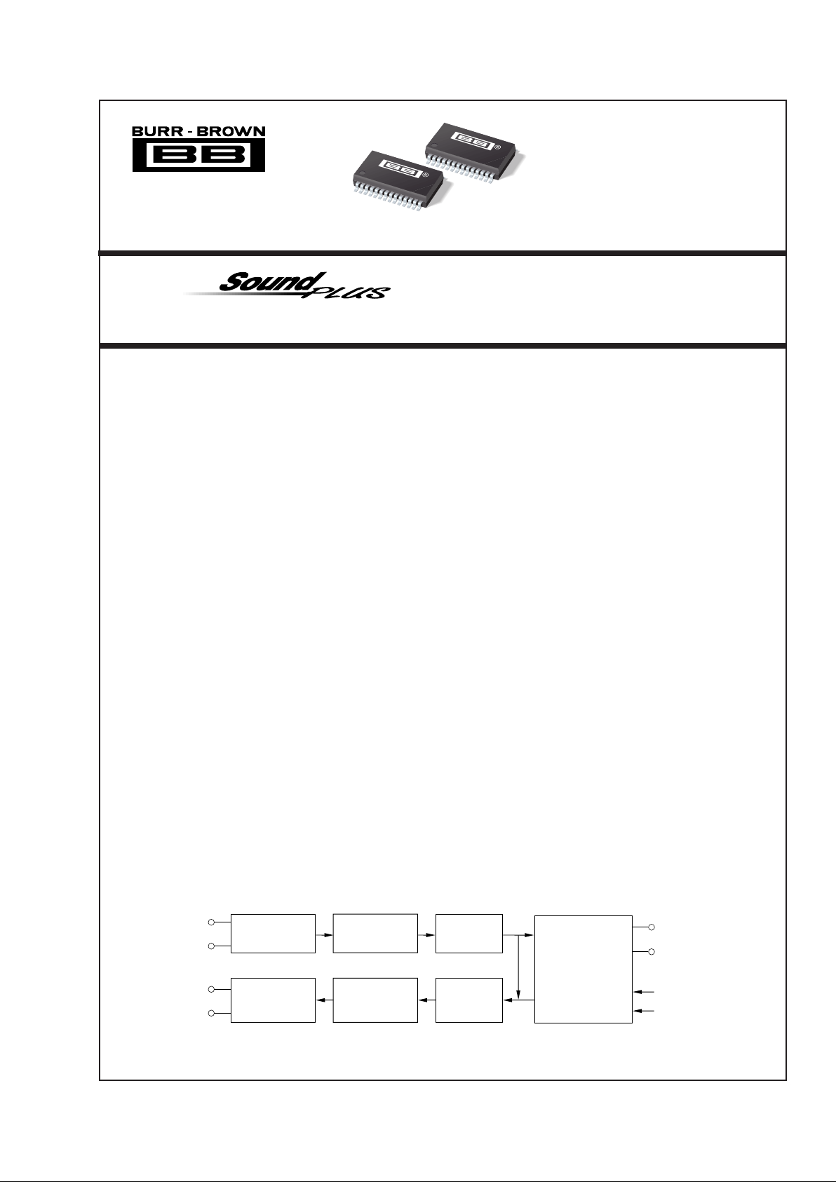
The PCM3000/3001 is a low cost single chip stereo
audio CODEC (analog-to-digital and digital-to-analog
converter) with single-ended analog voltage input and
output.
Both ADCs and DACs employ delta-sigma modulation with 64X oversampling. The ADCs include a
digital decimation filter and the DACs include an 8X
oversampling digital interpolation filter. The DACs
also include digital attenuation, de-emphasis, infinite
zero detection and soft mute to form a complete
subsystem. The PCM3000/3001 operates with leftjustified, right-justified, I2S or DSP data formats.
PCM3000 can be programmed with a 3-wire serial
interface for special features and data formats.
PCM3001 can be pin-programmed for data formats.
Fabricated on a highly advanced CMOS process, the
PCM3000/3001 is suitable for a wide variety of costsensitive consumer applications where good performance is required. Applications include sampling keyboards, digital mixers, mini-disc recorders, hard-disk
recorders, karaoke systems, DSP-based car stereo,
DAT recorders, and video conferencing.
© 1996 Burr-Brown Corporation PDS-1342E Printed in U.S.A., January, 2000
International Airport Industrial Park • Mailing Address: PO Box 11400, Tucson, AZ 85734 • Street Address: 6730 S. Tucson Blvd., Tucson, AZ 85706 • Tel: (520) 746-1111
Twx: 910-952-1111 • Internet: http://www.burr-brown.com/ • Cable: BBRCORP • Telex: 066-6491 • FAX: (520) 889-1510 • Immediate Product Info: (800) 548-6132
For most current data sheet and other product
information, visit www.burr-brown.com
Lch In
Rch In
Analog Front-End
Delta-Sigma
Modulator
Digital
Decimation
Filter
Serial Interface
and
Mode Control
Digital Out
Digital In
Mode Control
System Clock
Lch Out
Rch Out
Low Pass Filter
and
Output Buffer
Multi-Level
Delta-Sigma
Modulator
Digital
Interpolation
Filter
®
2
PCM3000/3001
SPECIFICATIONS
All specifications at +25°C, VDD = V
CC
= +5V, fS = 44.1kHz, SYSCLK = 384fS, CLKIO Input, 18-bit data, unless otherwise noted.
The information provided herein is believed to be reliable; however, BURR-BROWN assumes no responsibility for inaccuracies or omissions. BURR-BROWN assumes no
responsibility for the use of this information, and all use of such information shall be entirely at the user’s own risk. Prices and specifications are subject to change without notice.
No patent rights or licenses to any of the circuits described herein are implied or granted to any third party. BURR-BROWN does not authorize or warrant any BURR-BROWN
product for use in life support devices and/or systems.
NOTES: (1) Pins 16, 17, 18, 22, 25, 26, 27, 28: LRCIN, BCKIN, DIN, CLKIO, MC/FMT2, MD/FMT1, ML/FMT0, RSTB. (2) Pins 16, 17, 18, 22: LRCIN, BCKIN, DIN,
CLKIO (Schmitt Trigger Input). (3) Pins 25, 26, 27, 28: MC/FMT2, MD/FMT1, ML/FMT0, RSTB (Schmitt Trigger Input, 70kΩ Internal Pull-Up Resistor). (4) Pin 20:
XTI. (5) Pins 19, 22: DOUT,CLKIO. (6) Pin 21: XTO. (7) Refer to Application Bulletin AB-148 for information relating to operation at lower sampling frequencies.
(8) High Pass Filter disabled (PCM3000 only) to measure DC offset. (9) f
IN
= 1kHz, using Audio Precision System II, rms mode with 20kHz LPF, 400Hz HPF used
for performance calculation. (10) With no load on XTO and CLKIO.
PCM3000E/3001E
PARAMETER CONDITIONS MIN TYP MAX UNITS
DIGITAL INPUT/OUTPUT
Input Logic
Input Logic Level: V
IH
(1)
2.0 VDC
V
IL
(1)
0.8 VDC
Input Logic Current: I
IN
(2)
±1 µA
Input Logic Current: I
IN
(3)
–120 µA
Input Logic Level: V
IH
(4)
0.64 • V
DD
VDC
V
IL
(4)
0.28 • V
DD
VDC
Input Logic Current: I
IN
(4)
±40 µA
Output Logic
Output Logic Level: V
OH
(5)
I
OUT
= –1.6mA 4.5 VDC
V
OL
(5)
I
OUT
= +3.2mA 0.5 VDC
Output Logic Level: V
OH
(6)
I
OUT
= –3.2mA 4.5 VDC
V
OL
(6)
I
OUT
= +3.2mA 0.5 VDC
CLOCK FREQUENCY
Sampling Frequency (f
S
) 32
(7)
44.1 48 kHz
System Clock Frequency 256f
S
8.1920 11.2896 12.2880 MHz
384f
S
12.2880 16.9344 18.4320 MHz
512f
S
16.3840 22.5792 24.5760 MHz
ADC CHARACTERISTICS
RESOLUTION 18 Bits
DC ACCURACY
Gain Mismatch Channel-to-Channel ±1.0 ±5.0 % of FSR
Gain Error ±2.0 ±5.0 % of FSR
Gain Drift ±20 ppm of FSR/°C
Bipolar Zero Error High-Pass Filter Off
(8)
±1.7 %of FSR
Bipolar Zero Drift High-Pass Filter Off
(8)
±20 ppm of FSR/°C
DYNAMIC PERFORMANCE
(9)
THD+N: VIN = –0.5dB f = 1kHz –88 –80 dB
V
IN
= –60dB f = 1kHz –31 dB
Dynamic Range f = 1kHz, A-Weighted 90 94 dB
Signal-to-Noise Ratio f = 1kHz, A-Weighted 90 94 dB
Channel Separation 88 92 dB
DIGITAL FILTER PERFORMANCE
Passband 0.454f
S
Hz
Stopband 0.583f
S
Hz
Passband Ripple ±0.05 dB
Stopband Attenuation –65 dB
Delay Time (Latency) 17.4/f
S
sec
DIGITAL HIGH PASS FILTER RESPONSE
–3dB Frequency 0.019f
S
mHz
ANALOG INPUT
Voltage Range 0dB (Full Scale) 2.9 Vp-p
Center Voltage 2.1 V
Input Impedance 15 kΩ
ANTI-ALIASING FILTER
–3dB Frequency C
EXT
= 470pF 170 kHz
®
3 PCM3000/3001
PCM3000E/3001E
PARAMETER CONDITIONS MIN TYP MAX UNITS
SPECIFICATIONS (cont.)
All specifications at +25°C, VDD = V
CC
= 5V, fS = 44.1kHz, SYSCLK = 384fS, CLKIO Input, 18-bit data, unless otherwise noted.
Supply Voltage
+V
DD
, +VCC1, +VCC2 ...................................................................... +6.5V
Supply Voltage Differences...............................................................±0.1V
GND Voltage Differences..................................................................±0.1V
Digital Input Voltage......................................................–0.3 to V
DD
+ 0.3V
Analog Input Voltage.........................................–0.3 to V
CC1, VCC
2 + 0.3V
Power Dissipation .......................................................................... 300mW
Input Current ................................................................................... ±10mA
Operating Temperature Range ......................................... –25°C to +85°C
Storage Temperature...................................................... –55°C to +125°C
Lead Temperature (soldering, 5s).................................................. +260°C
(reflow, 10s) ..................................................... +235°C
Thermal Resistance,
θ
JA
.............................................................. 100°C/W
ABSOLUTE MAXIMUM RATINGS
ELECTROSTATIC
DISCHARGE SENSITIVITY
This integrated circuit can be damaged by ESD. Burr-Brown
recommends that all integrated circuits be handled with
appropriate precautions. Failure to observe proper handling
and installation procedures can cause damage.
ESD damage can range from subtle performance degradation to complete device failure. Precision integrated circuits
may be more susceptible to damage because very small
parametric changes could cause the device not to meet its
published specifications.
DAC CHARACTERISTICS
RESOLUTION 18 Bits
DC ACCURACY
Gain Mismatch Channel-to-Channel ±1.0 ±5.0 % of FSR
Gain Error ±1.0 ±5.0 % of FSR
Gain Drift ±20 ppm of FSR/°C
Bipolar Zero Error ±1.0 % of FSR
Bipolar Zero Drift ±20 ppm of FSR/°C
DYNAMIC PERFORMANCE
(9)
THD+N: V
OUT
= 0dB (Full Scale) –90 –80 dB
V
OUT
= –60dB –34 dB
Dynamic Range EIAJ A-Weighted 90 97 dB
Signal-to-Noise Ratio (Idle Channel) EIAJ A-Weighted 92 98 dB
Channel Separation 90 95 dB
DIGITAL FILTER PERFORMANCE
Passband 0.445f
S
Hz
Stopband 0.555f
S
Hz
Passband Ripple ±0.17 dB
Stopband Attenuation –35 dB
Delay Time 11.1/f
S
sec
ANALOG OUTPUT
Voltage Range 0.62 • V
CC
Vp-p
Center Voltage 0.5 • V
CC
VDC
Load Impedance AC Load 5 kΩ
ANALOG LOW PASS FILTER
Frequency Response f = 20kHz –0.16 dB
POWER SUPPLY REQUIREMENTS
Voltage Range: V
CC
4.5 5 5.5 VDC
V
DD
4.5 5 5.5 VDC
Supply Current: +I
CC
, +I
DD
(10)
VCC = VDD = 5V 32 50 mA
Power Dissipation V
CC
= VDD = 5V 160 250 mW
TEMPERATURE RANGE
Operation –25 +85 °C
Storage –55 +125 °C
PACKAGE SPECIFIED
DRAWING TEMPERATURE PACKAGE ORDERING TRANSPORT
PRODUCT PACKAGE NUMBER RANGE MARKING NUMBER
(1)
MEDIA
PCM3000E SSOP-28 324 –25°C to +85°C PCM3000E PCM3000E Rails
" " " " " PCM3000E/2K Tape and Reel
PCM3001E SSOP-28 324 –25°C to +85°C PCM3001E PCM3001E Rails
" " " " " PCM3001E/2K Tape and Reel
NOTES: (1) Models with a slash (/) are available only in Tape and Reel in the quantities indicated (e.g., /2K indicates 2000 devices per reel). Ordering 2000 pieces
of “PCM3000E/2K” will get a single 2000-piece Tape and Reel.
PACKAGE/ORDERING INFORMATION
®
4
PCM3000/3001
VINL
V
CC
1
AGND1
V
REF
L
V
REF
R
V
IN
R
C
IN
PR
C
IN
NR
C
IN
NL
C
IN
PL
VCOM
V
OUT
R
AGND2
V
CC
2
RSTB
FMT0
FMT1
FMT2
DGND
V
DD
CLKIO
XTO
XTI
DOUT
DIN
BCKIN
LRCIN
V
OUT
L
1
2
3
4
5
6
7
8
9
10
11
12
13
14
28
27
26
25
24
23
22
21
20
19
18
17
16
15
VINL
V
CC
1
AGND1
V
REF
L
V
REF
R
V
IN
R
C
IN
PR
C
IN
NR
C
IN
NL
C
IN
PL
VCOM
V
OUT
R
AGND2
V
CC
2
RSTB
ML
MD
MC
DGND
V
DD
CLKIO
XTO
XTI
DOUT
DIN
BCKIN
LRCIN
V
OUT
L
1
2
3
4
5
6
7
8
9
10
11
12
13
14
28
27
26
25
24
23
22
21
20
19
18
17
16
15
PIN CONFIGURATION—PCM3000
Top View SSOP
PIN CONFIGURATION—PCM3001
Top View SSOP
PIN NAME I/O DESCRIPTION
1V
IN
L IN ADC Analog Input, Lch
2V
CC
1 — ADC Analog Power Supply
3 AGND1 — ADC Analog Ground
4V
REF
L — ADC Input Reference, Lch
5V
REF
R — ADC Input Reference, Rch
6V
IN
R IN ADC Analog Input, Rch
7C
IN
PR — ADC Anti-alias Filter Capacitor (+), Rch
8C
IN
NR — ADC Anti-alias Filter Capacitor (–), Rch
9C
IN
NL — ADC Anti-alias Filter Capacitor (–), Lch
10 C
IN
PL — ADC Anti-alias Filter Capacitor (+), Lch
11 VCOM — DAC Output Common
12 V
OUT
R OUT DAC Analog Output, Rch
13 AGND2 — DAC Analog Ground
14 V
CC
2 — DAC Analog Power Supply
15 V
OUT
L OUT DAC Analog Output, Lch
16 LRCIN IN Sample Rate Clock Input (f
S
)
(2)
17 BCKIN IN Bit Clock Input
(2)
18 DIN IN Data Input
(2)
19 DOUT OUT Data Output
20 XTI IN Oscillator Input
21 XTO OUT Oscillator Output
22 CLKIO I/O Buffered Output of Oscillator or External Clock
Input
(2)
23 V
DD
— Digital Power Supply
24 DGND — Digital Ground
25 MC/FMT2 IN Serial Control Bit Clock (PCM3000)/Data
Format Control 2 (PCM3001)
(1, 2)
26 MD/FMT1 IN Serial Control Data (PCM3000)/Data Format
Control 1 (PCM3001)
(1, 2)
27 ML/FMT0 IN Serial Control Strobe Pulse/Data Format
Control 0 (PCM3001)
(1, 2)
28 RSTB IN Reset
(1, 2)
NOTES: (1) With 70kΩ typical internal pull-up resistor. (2) Schmitt trigger input.
PIN ASSIGNMENTS PCM3000/3001
®
5 PCM3000/3001
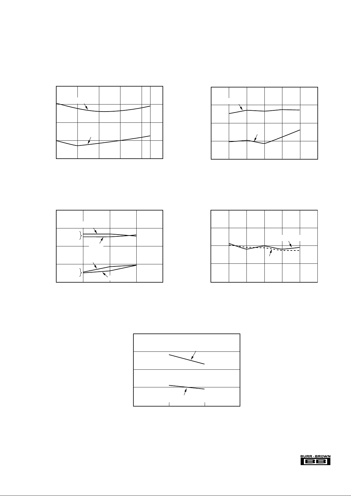
TYPICAL PERFORMANCE CURVES
ADC SECTION
At TA = +25°C, V
CC
= V
DD
= +5V, fIN = 1.0kHz, fS = 44.1kHz, 18-bit data, VIN = 2.9Vp-p, and SYSCLK = 384fS, unless otherwise noted.
THD+N vs TEMPERATURE
Temperature (°C)
THD+N at 0dB (%)
0.01
0.008
0.006
0.004
0.002
–25 0 25 50 75 85 100
THD+N at –60dB (%)
4.0
3.0
2.0
1.0
0
–60dB
0dB
THD+N vs POWER SUPPLY
V
CC
(V)
THD+N at 0dB (%)
0.01
0.008
0.006
0.004
0.002
4.5 4.75 5.0 5.25 5.5
THD+N at –60dB (%)
4.0
3.0
2.0
1.0
0
–60dB
0dB
THD+N vs SYSTEM CLOCK
and SAMPLING FREQUENCY
System Clock
THD+N at 0dB (%)
0.01
0.008
0.006
0.004
0.002
256f
S
384f
S
512f
S
THD+N at –60dB (%)
4.0
3.0
2.0
1.0
0
44.1kHz
44.1kHz
48kHz
48kHz
–60dB
0dB
SNR and DYNAMIC RANGE vs POWER SUPPLY
V
CC
(V)
SNR (dB)
98
96
94
92
90
4.5 4.75 5.0 5.25 5.50
Dynamic Range (dB)
98
96
94
92
90
SNR
Dynamic Range
THD+N vs OUTPUT DATA RESOLUTION
Resolution
THD+N at 0dB (%)
THD+N at –60dB (%)
0.01
0.008
0.006
0.004
0.002
16-Bit 18-Bit
4.0
3.0
2.0
1.0
0
0dB
–60dB
®
6
PCM3000/3001
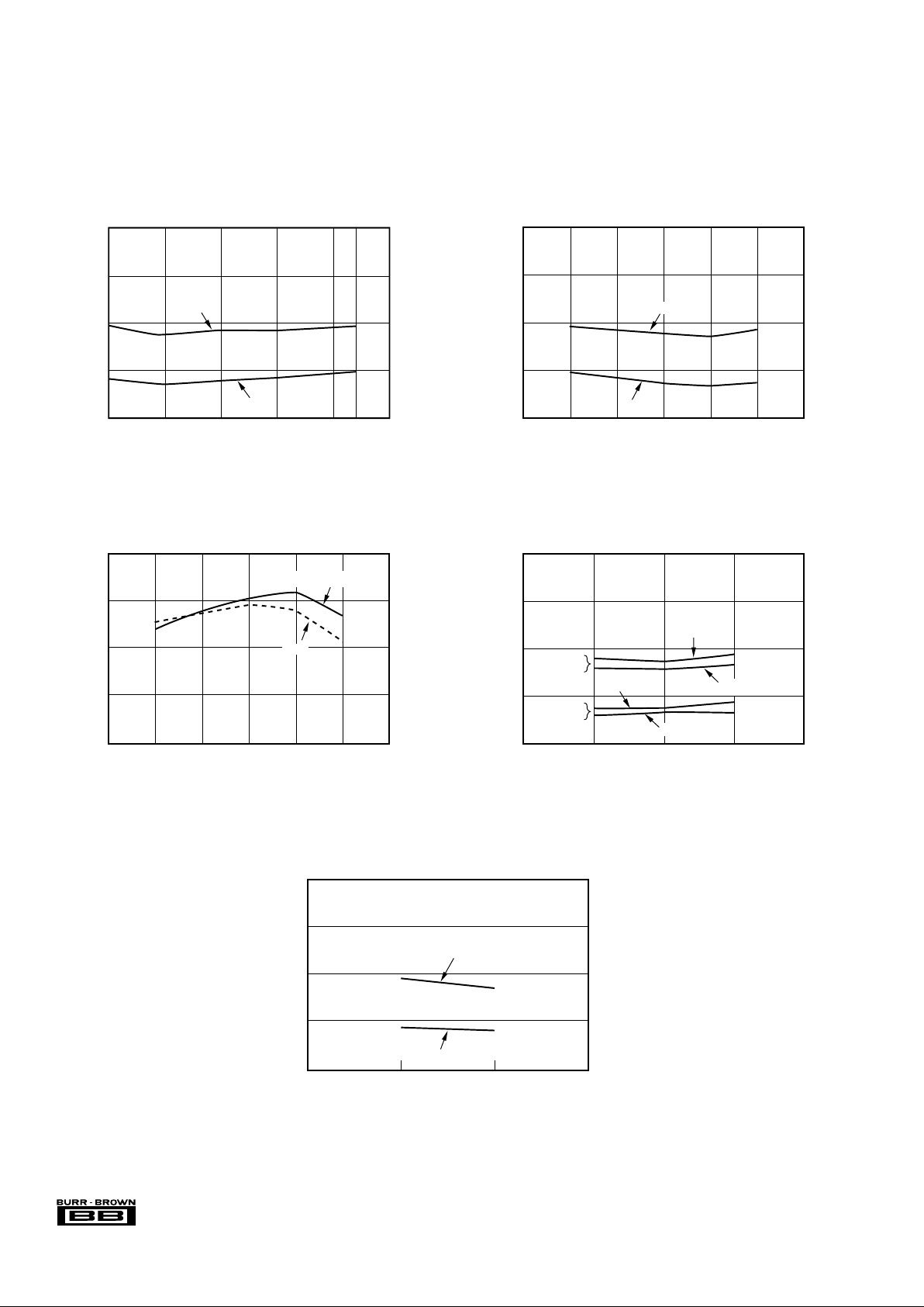
TYPICAL PERFORMANCE CURVES
DAC SECTION
At TA = +25°C, V
CC
= V
DD
= +5V, fIN = 1.0kHz, fS = 44.1kHz, 18-bit data, and SYSCLK = 384fS, unless otherwise noted.
THD+N vs TEMPERATURE
Temperature (°C)
THD+N at 0dB (%)
0.01
0.008
0.006
0.004
0.002
–25 0 25 50 75 85 100
THD+N at –60dB (%)
4.0
3.0
2.0
1.0
0
–60dB
0dB
THD+N vs POWER SUPPLY
V
CC
(V)
THD+N at 0dB (%)
0.01
0.008
0.006
0.004
0.002
4.5 4.75 5.0 5.25 5.5
THD+N at –60dB (%)
4.0
3.0
2.0
1.0
0
–60dB
0dB
SNR and DYNAMIC RANGE vs POWER SUPPLY
V
CC
(V)
SNR (dB)
100
98
96
94
92
4.5 4.75 5.0 5.25 5.50
Dynamic Range (dB)
100
98
96
94
92
Dynamic Range
SNR
THD+N vs SYSTEM CLOCK
and SAMPLING FREQUENCY
System Clock
THD+N at 0dB (%)
0.01
0.008
0.006
0.004
0.002
256f
S
384f
S
512f
S
THD+N at –60dB (%)
4.0
3.0
2.0
1.0
0
44.1kHz
44.1kHz
48kHz
48kHz
–60dB
0dB
THD+N vs INPUT DATA RESOLUTION
Resolution
THD+N at 0dB (%)
THD+N at –60dB (%)
0.01
0.008
0.006
0.004
0.002
16-Bit 18-Bit
4.0
3.0
2.0
1.0
0
0dB
–60dB
®
7 PCM3000/3001
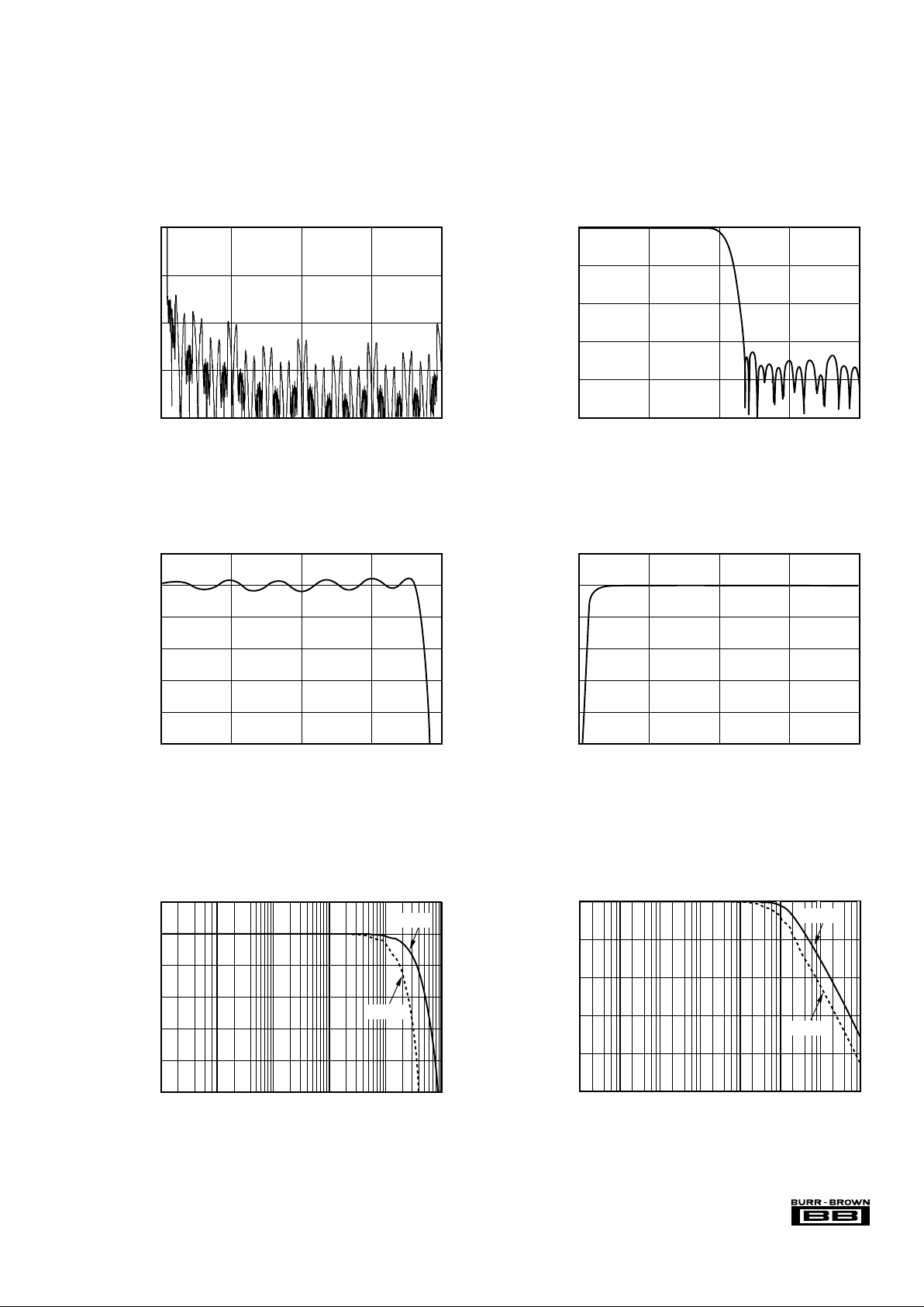
HIGH PASS FILTER RESPONSE
Normalized Frequency (x f
S
/1000 Hz)
Amplitude (dB)
0.2
0.0
–0.2
–0.4
–0.6
–0.8
–1.0
12340
TYPICAL PERFORMANCE CURVES
At TA = +25°C, V
CC
= V
DD
= +5V, and SYSCLK = 384fS, unless otherwise noted.
ADC DIGITAL FILTER
STOPBAND ATTENUATION CHARACTERISTICS
Normalized Frequency (x f
S
Hz)
Amplitude (dB)
0
–20
–40
–60
–80
–100
0.25 0.50 0.75 1.000
PASSBAND RIPPLE CHARACTERISTICS
Normalized Frequency (x f
S
Hz)
Amplitude (dB)
0.2
0.0
–0.2
–0.4
–0.6
–0.8
–1.0
0.125 0.250 0.375 0.5000
OVERALL CHARACTERISTICS
Normalized Frequency (x f
S
Hz)
Amplitude (dB)
0
–50
–100
–150
–200
81624320
ANTI-ALIASING FILTER PASSBAND
FREQUENCY RESPONSE (C
EXT
= 470pF, 1000pF)
Frequency (Hz)
Amplitude (dB)
0.2
0.0
–0.2
–0.4
–0.6
–0.8
–1.0
10 100 1k 10k 100k0
470pF
1000pF
ANTI-ALIASING FILTER OVERALL
FREQUENCY RESPONSE (C
EXT
= 470pF, 1000pF)
Frequency (Hz)
Amplitude (dB)
0
–10
–20
–30
–40
–50
10 100 1k 10k 100k 1M 10M0
470pF
1000pF
ANTI-ALIASING FILTER
 Loading...