

Burr Brown PCM2702E, PCM2702E-2K Datasheet
1
®
PCM2702
®
PCM2702
16-Bit Stereo
DIGITAL-TO-ANALOG CONVERTER
with Interface
FEATURES
● INTEGRATED USB INTERFACE:
Full-Speed Transceiver Supports 12Mbps
Data Transfer.
Fully Compliant with the USB 1.0 Specifi-
cation.
Adaptive Mode for Isochronous Transfer.
Self-Powered Device.
● ACCEPTS 16-BIT STEREO AND MONO
USB AUDIO DATA STREAMS.
● ANALOG PERFORMANCE (VCC = 5V):
Dynamic Range: 100dB (typ at 16-bit)
SNR: 105dB (typ)
THD+N: 0.002% (typ at 16-bit)
Full-Scale Output: 3.1Vp-p
● 8X OVERSAMPLING DIGITAL FILTER:
Passband: 0.454f
S
Stopband: 0.546f
S
Passband Ripple: ±0.002dB
Stopband Attenuation: –82dB
● SAMPLING RATE (FS): 32kHz, 44.1kHz,
48kHz
● ON-CHIP CLOCK GENERATOR
WITH SINGLE 12MHz CLOCK SOURCE
● MULTI-FUNCTIONS:
Digital Attenuator:
0dB to –64dB, 1dB/step
Soft Mute
Zero Flag
Suspend Flag
Playback Flag
● DUAL POWER SUPPLIES:
+5V for Analog portion
+3.3V for Digital portion
● PACKAGE: SSOP-28
DESCRIPTION
The PCM2702 is a single chip digital-to-analog converter offering two D/A output channels and an integrated USB 1.0 compliant interface controller. The
newly developed SpAct™ (Sampling Period Adaptive
Controlled Tracking) system recovers a stable, lowjitter clock for internal PLL and DAC operation from
the USB interface audio data.
The PCM2702 is based upon Burr-Brown’s Enhanced
Multi-level Delta-Sigma Modulator, an 8x
oversampling digital interpolation filter, and an analog
output low-pass filter.
The PCM2702 can accept a 48kHz, 44.1kHz and
32kHz sampling rates, using either 16-bit stereo or
monaural audio data. Digital attenuation and softmute features are included, and are controlled via USB
audio class request.
Patents Pending.
SpAct™ is a trademark of Burr-Brown Corporation.
©
2000 Burr-Brown Corporation PDS-1584A Printed in U.S.A. May, 2000
International Airport Industrial Park • Mailing Address: PO Box 11400, Tucson, AZ 85734 • Street Address: 6730 S. Tucson Blvd., Tucson, AZ 85706 • Tel: (520) 746-1111
Twx: 910-952-1111 • Internet: http://www.burr-brown.com/ • Cable: BBRCORP • Telex: 066-6491 • FAX: (520) 889-1510 • Immediate Product Info: (800) 548-6132
For most current data sheet and other product
information, visit www.burr-brown.com
APPLICATIONS
●
STAND-ALONE USB AUDIO SPEAKERS
●
CRT/LCD INTEGRATED USB AUDIO SPEAKERS
●
USB AUDIO AMPLIFIERS
●
OTHER USB AUDIO APPLICATIONS
PCM2702
2
®
PCM2702
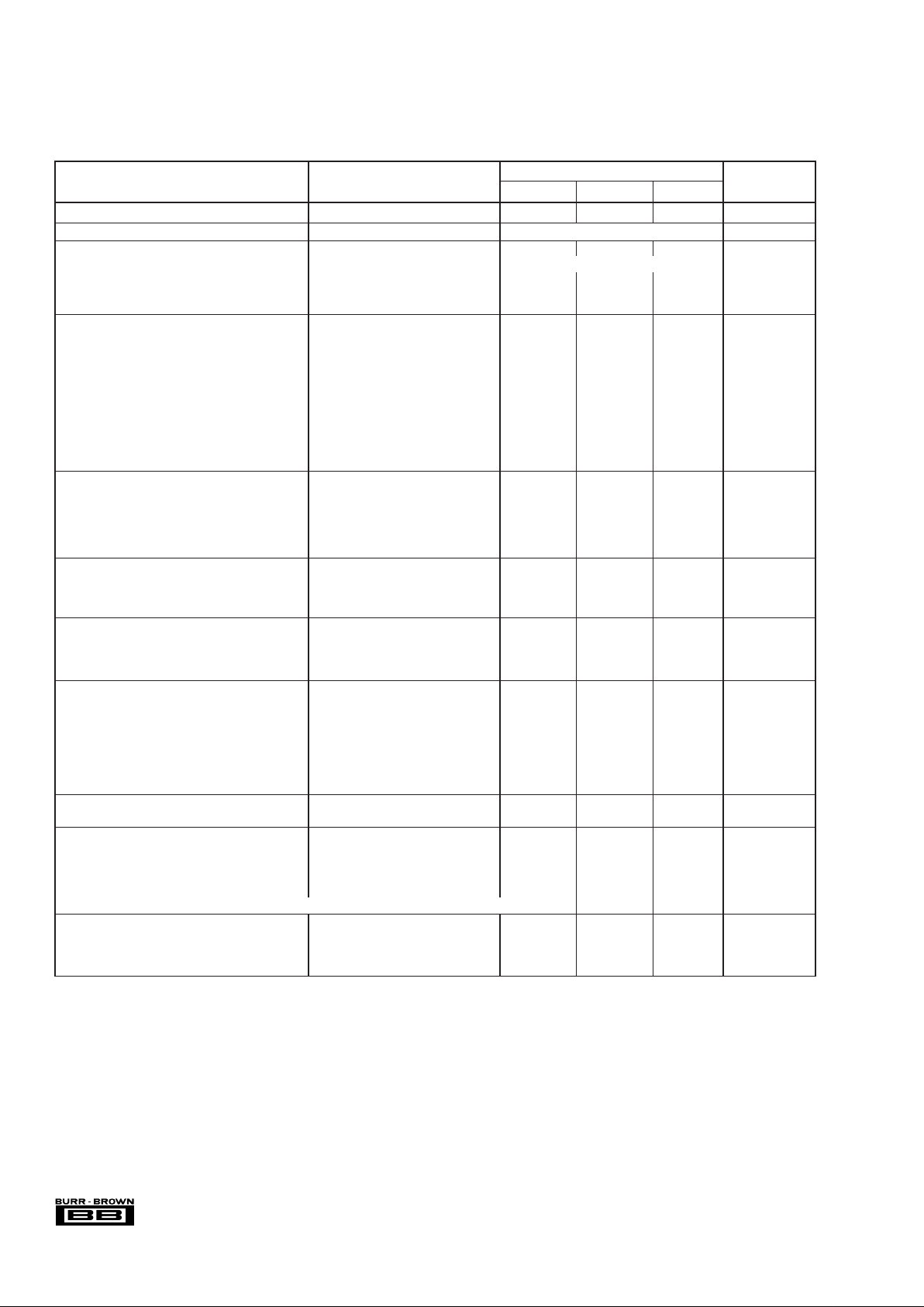
SPECIFICATIONS
At TA = +25°C, VCC = VCCL = VCCR = VCCP = 5.0V, VDD = VDDC = 3.3V, fS = 44.1MHz, signal frequency = 1kHz and 16-bit data, unless otherwise specified.
PCM2702E
PARAMETER CONDITIONS MIN TYP MAX UNITS
RESOLUTION 16 Bits
HOST INTERFACE Supports USB revision 1.0, Full Speed
DIGITAL FORMAT
Audio Data Format USB ISOCHRONOUS OUT
Audio Data Bit Length 16
Audio Data Channel 1, 2
Sampling Frequency (f
S
) 32, 44.1, 48
DIGITAL INPUT/OUTPUT
Input Logic Level V
IH
(1)
2.0 VDC
V
IL
(1)
0.8 VDC
V
IH
(2)
0.7 V
DD
VDC
V
IL
(2)
0.7 V
DD
VDC
Input Logic Current I
IH
(1)
VIN = V
DD
+65 +100 µA
I
IL
(1)
VIN = 0V ±10 µA
I
IH
(2)
VIN = V
DD
±10 µA
I
IL
(2)
VIN = 0V ±10 µA
Output Logic Level V
OH
(3)
IOH = –1mA 2.8 VDC
V
OL
(3)
IOL = +1mA 0.5 VDC
DYNAMIC PERFORMANCE
(4)
THD+N at V
OUT
= 0dB 0.002 0.005 %
THD+N at V
OUT
= –60dB 1.2 %
Dynamic Range EIAJ, A-Weighted 96 100 dB
SIgnal-to-Noise Ratio EIAJ, A-Weighted 100 105 dB
Channel Seperation 98 103 dB
DC ACCURACY
Gain Error ±1.0 ±3.0 % of FSR
Gain Mismatch, Channel-to-Channel ±1.0 ±3.0 % of FSR
Bipolar Zero Error V
OUT
= 0.5 VCC at BPZ ±30 ±60 mV
ANALOG OUTPUT
Output Voltage Full-Scale(–0dB) 62% of V
CC
Vp-p
Center Voltage 50% of V
CC
VDC
Load Impedance AC-Load 5 kΩ
DIGITAL FILTER PERFORMANCE
Passband ±0.002dB 0.454f
S
Passband –3dB 0.490f
S
Stopband 0.546f
S
Passband Ripple ±0.002 dB
Stopband Attenuation Stopband = 0.546f
S
–75 dB
Stopband Attenuation Stopband = 0.567f
S
–82 dB
Delay Time 34/f
S
11 s
ANALOG FILTER PERFORMANCE
Frequency Response at 20kHz ≠0.02 dB
POWER SUPPLY REQUIREMENTS
Voltage Range V
DD
, VDDC +3.0 +3.3 +3.6 VDC
V
CC
, VCCL, VCCR, VCCP +4.5 +5.0 +5.5 VDC
Supply Current I
DD
VDD = VDDC = 3.3V 22 30 mA
I
CCVCC
= VCCL = VCCR = VCCP = 5.0V 18 25 mA
Power Dissipation
VDD = VDDC = 3.3V, and VCC = VCCL = VCCR = VCCP = 5.0V
165 225 mW
TEMPERATURE RANGE
Operation Temperature 070°C
Storage Temperature –55 +125 °C
Thermal Resistance,
θ
JA
SSOP-28 100 °C/W
NOTES: (1) Pins 8, 13, 14, 15, 16: V
BUS
, TEST3 TEST2 TEST1, TEST0. (2) Pin1: XTI. (3) Pins 10, 11, 12, 28: PLYBCK, SSPND, ZERO, XTO. (4) The dynamic
performance is based upon ideal host signal quality, and may vary according to the system. Dynamic performance specifications are tested using a Shibasoku #725
THD Meter with 400Hz HPF, 30kHz LPF, Average Mode, and 20kHz Bandwidth limiting. The load connected to the analog output is 5kΩ, or larger, via AC coupling.
The information provided herein is believed to be reliable; however, BURR-BROWN assumes no responsibility for inaccuracies or omissions. BURR-BROWN
assumes no responsibility for the use of this information, and all use of such information shall be entirely at the user’s own risk. Prices and specifications are subject
to change without notice. No patent rights or licenses to any of the circuits described herein are implied or granted to any third party. BURR-BROWN does not
authorize or warrant any BURR-BROWN product for use in life support devices and/or systems.
3
®
PCM2702
Supply Voltage
(2)
.............................................................................................................. +6.5V
Supply Voltage
(3)
.............................................................................................................. +4.0V
Supply Voltage Differences
(4)
.................................................................................. ±0.1V
Supply Voltage Differences
(5)
.................................................................................. ±0.1V
Ground Voltage Differences
(6)
................................................................................. ±0.1V
Digital Input Voltage
(7)
................................................................. –0.3V to V
DD
+ 0.3V
Digital Input Voltage
(8)
................................................................................ –0.3V to 6.5V
Analog Input Voltage ................................................ –0.3V to V
CC
+ 0.3V
Input Current (any pins except supplies) ....................................... ±10mA
Operating Temperature .................................................. –25°C to +85°C
Storage Temperature ..................................................... –55°C to +125°C
Junction Temperature .................................................................... +150°C
Lead Temperature (soldering, 5s) ................................................. +260°C
Package Temperature (IR reflow, peak, 10s) ............................... +235°C
NOTES: (1) Stresses above those listed under Absolute Maximum Ratings
may cause permanent damage to the device. Exposure to absolute maximum
conditions for extended periods may affect device reliability.
(2) V
CC
, VCCL, VCCR, VDDP. (3) VDD, VDDC. (4) Among VCC, VCCL, VCCR, VCCP.
(5) Among V
DD
, VDDC. (6) Among AGND, AGNDL, AGNDR, AGNDP, DGND,
DGNDC, and DGNDU. (7) XTI, D+, D–, PLYBCK, SSPND, ZERO, XTO.
(8) V
BUS
, TEST#, TEST2, TEST1, TEST0.
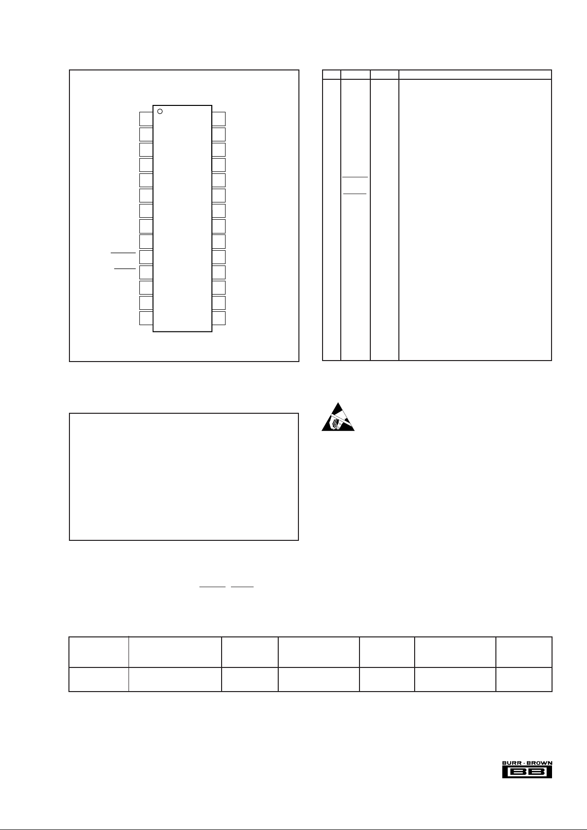
ABSOLUTE MAXIMUM RATINGS
(1)
ELECTROSTATIC
DISCHARGE SENSITIVITY
This integrated circuit can be damaged by ESD. Burr-Brown
recommends that all integrated circuits be handled with
appropriate precautions. Failure to observe proper handling
and installation procedures can cause damage.
ESD damage can range from subtle performance degradation to complete device failure. Precision integrated circuits
may be more susceptible to damage because very small
parametric changes could cause the device not to meet its
published specifications.
PACKAGE SPECIFIED
DRAWING TEMPERATURE PACKAGE ORDERING TRANSPORT
PRODUCT PACKAGE NUMBER RANGE MARKING NUMBER
(1)
MEDIA
PCM2702E SSOP-28 324 0°C to +70°C PCM2702E PCM2702E Rails
"""""PCM2702E/2K Tape and Reel
NOTE: (1) Models with a slash (/) are available only in Tape and Reel in the quantities indicated (e.g., /2K indicates 2000 devices per reel). Ordering 2000 pieces
of “PCM2702E/2K” will get a single 2000-piece Tape and Reel.
PACKAGE /ORDERING INFORMATION
PIN NAME TYPE DESCRIPTIONS
1 XTI IN Crystal Oscillator Input.
(1)
2VDDC — Digital Power Supply for Clock Generator,
+3.3V.
3 DGNDC — Digital Ground for Clock Generator.
4V
DD
— Digital Power Supply, +3.3V.
5 DGND — Digital Ground.
6 D+ IN/OUT USB Differential Input/Output Plus.
7 D– IN/OUT USB Differential Input/Output Minus.
8V
BUS
IN USB Bus Power (this pin NEVER consumes
USB bus power).
(2)
9 DGNDU — Digital Ground for USB Transceiver.
10 PLYBCK OUT Playback flag, active LOW (LOW: playback,
HIGH: idle).
11 SSPND OUT Suspend flag, active LOW (LOW: suspend,
HIGH: operational).
12 ZERO OUT Zero flag (LOW: Normal, HIGH: ZERO.)
13 TEST3 IN Test pin 3. Connect to digital ground.
(2)
14 TEST2 IN Test pin 2. Connect to digital ground.
(2)
15 TEST1 IN Test pin 1. Connect to digital ground.
(2)
16 TEST0 IN Test pin 0. Connect to digital ground.
(2)
17 VCCR — Analog Supply for R-channel, +5V.
18 AGNDR — Analog Ground for R-channel.
19 V
OUT
R OUT Analog Output for R-channel.
20 AGND — Analog Ground.
21 V
COM
— DC Common-Mode Voltage for DAC.
22 V
CC
— Analog Supply, +5V.
23 V
OUT
L OUT Analog Output for L-channel.
24 AGNDL — Analog Ground for L-channel.
25 V
CC
L — Analog Supply for L-channel, +5V.
26 AGNDP — Analog Ground for PLL.
27 V
CC
P — Analog Supply for PLL, +5V.
28 XTO OUT Crystal Oscillator Output.
NOTES: (1) 3.3 V tolerant. (2) Schmitt trigger input with internal pull-down,
5V tolerant.
XTI
V
DD
C
DGNDC
V
DD
DGND
D+
D–
V
BUS
DGNDU
PLYBCK
SSPND
ZERO
TEST3
TEST2
XTO
V
CC
P
AGNDP
V
CC
L
AGNDL
V
OUT
L
V
CC
V
COM
AGND
V
OUT
R
AGNDR
V
CC
R
TEST0
TEST1
1
2
3
4
5
6
7
8
9
10
11
12
13
14
28
27
26
25
24
23
22
21
20
19
18
17
16
15
PCM2702
Top View SSOP
4
®
PCM2702
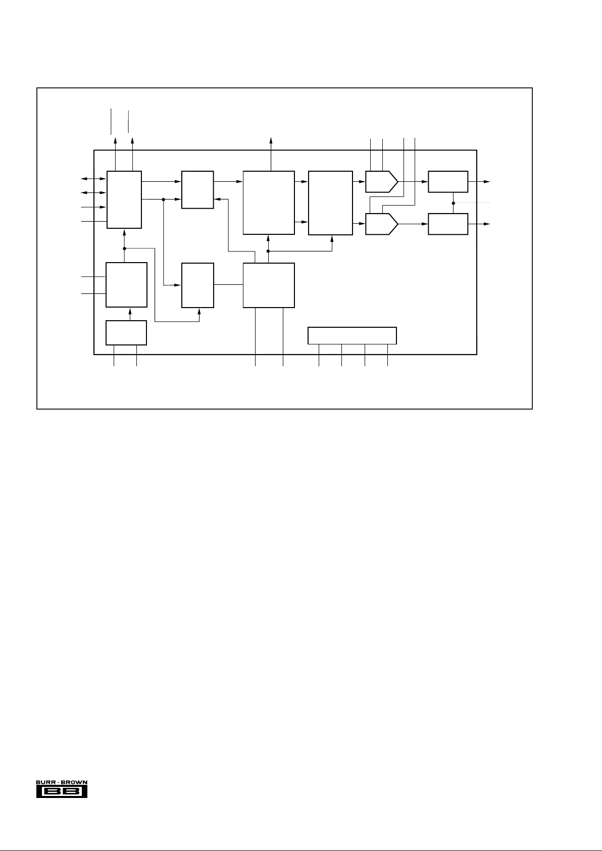
BLOCK DIAGRAM
DAC
DAC
SpAct™
Audio
Clock
Generator
8x
Oversampling
Digital Filter
Multi-
Level
DeltaSigma
Modulator
USB
I/F
Low-Pass
Filter
Low-Pass
Filter
Power Supply
Crystal
OSC
FIFO
mclk
System Clock
wrclk
USB
Packet
Data
Audio
Data
V
OUT
L
V
COM
V
OUT
R
rdclk
USB
Clock
Generator
PLYBCK
VDDP DGNDPXTI XTO VCCAGND VDDDGND
D+
D–
V
BUS
VDDC
DGNDU
DGNDC
SSPND
ZERO
V
CC
L
AGNDL
V
CC
R
AGNDR
 Loading...