

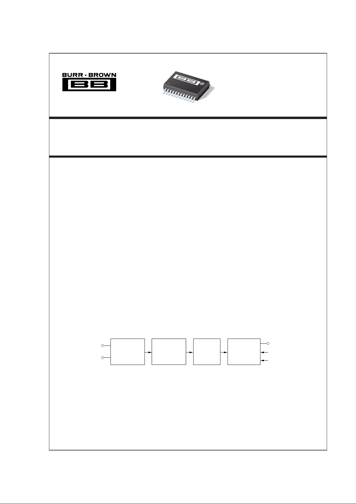
Burr Brown PCM1800E, PCM1800E-2K Datasheet
®
1 PCM1800
49%
FPO
PCM1800
®
FEATURES
● DUAL 20-BIT MONOLITHIC ∆Σ ADC
● SINGLE-ENDED VOLTAGE INPUT
● 64X OVERSAMPLING DECIMATION FILTER:
Passband Ripple:
±0.05dB
Stopband Attenuation: –65dB
● HIGH PERFORMANCE:
THD+N: -88dB (typ)
SNR: 95dB (typ)
Dynamic Range: 95dB (typ)
Internal High Pass Filter
● PCM AUDIO INTERFACE:
Master/Slave Modes
4 Data Formats
● SAMPLING RATE: 32kHz, 44.1kHz, 48kHz
● SYSTEM CLOCK: 256f
S
, 384fS, or 512f
S
● SINGLE +5V POWER SUPPLY
● SMALL 24-PIN SSOP PACKAGE
DESCRIPTION
PCM1800 is a low cost, single chip stereo analog-todigital converter with single-ended analog voltage
inputs. The PCM1800 uses a delta-sigma modulator
with 64X oversampling, including a digital decimation filter and serial interface which supports both
Master and Slave Modes and four data formats.
PCM1800 is suitable for a wide variety of cost-sensitive consumer applications where high performance is
required.
PCM1800 is fabricated on a highly advanced CMOS
process.
© 1997 Burr-Brown Corporation PDS-1387 Printed in U.S.A. August, 1997
International Airport Industrial Park • Mailing Address: PO Box 11400, Tucson, AZ 85734 • Street Address: 6730 S. Tucson Blvd., Tucson, AZ 85706 • Tel: (520) 746-1111 • Twx: 910-952-1111
Internet: http://www.burr-brown.com/ • FAXLine: (800) 548-6133 (US/Canada Only) • Cable: BBRCORP • Telex: 066-6491 • FAX: (520) 889-1510 • Immediate Product Info: (800) 548-6132
Single-Ended Analog Input 20-Bit Stereo
ANALOG-TO-DIGITAL CONVERTER
PCM1800
Analog Input (L)
Analog Input (R)
Analog Front-End
Delta-Sigma
Modulator
Decimation
Digital
Filter
Serial Interface
and
Format Control
Digital Output
Mode/Format Control
System Clock
®
2
PCM1800
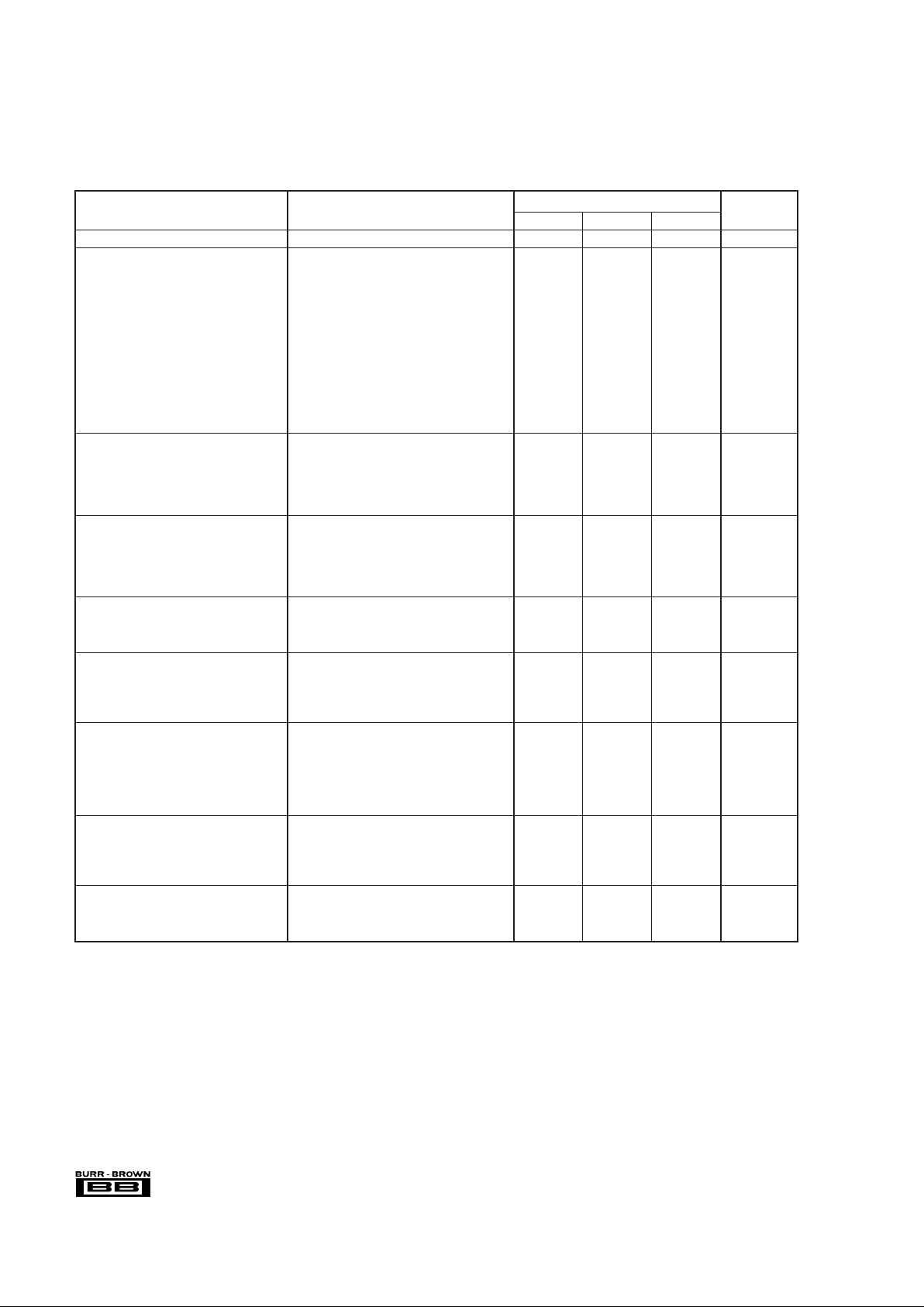
SPECIFICATIONS
All specifications at +25°C, +VDD = +V
CC
= +5V, fS = 44.1kHz, and 20-bit input data, SYSCLK = 384fS, unless otherwise noted.
PCM1800E
PARAMETER CONDITIONS MIN TYP MAX UNITS
RESOLUTION 20 Bits
DIGITAL INPUT/OUTPUT
Input Logic Level:
V
IH
(1)
2.0 V
V
IL
(1)
0.8 V
Input Logic Current:
I
IN
(2)
±1 µA
I
IN
(3)
+100 µA
Output Logic Level:
V
OH
(4)
IOH = –1.6mA 4.5 V
V
OL
(4)
IOL = +3.2mA 0.5 V
Sampling Frequency 32 44.1 48 kHz
System Clock Frequency 256f
S
8.1920 11.2896 12.2880 MHz
384f
S
12.2880 16.9344 18.4320 MHz
512f
S
16.3840 22.5792 24.5760 MHz
DC ACCURACY
Gain Mismatch Channel-to-Channel ±1.0 ±2.5 % of FSR
Gain Error ±2.0 ±5.0 % of FSR
Gain Drift ±20
ppm of FSR/°C
Bipolar Zero Error High Pass Filter Bypass ±2.0 % of FSR
Bipolar Zero Drift High Pass Filter Bypass ±20
ppm of FSR/°C
DYNAMIC PERFORMANCE
(5)
THD+N at FS (–0.5dB) –88 –80 dB
THD+N at –60dB –92 dB
Dynamic Range EIAJ, A-weighted 90 95 dB
Signal-To-Noise Ratio EIAJ, A-weighted 90 95 dB
Channel Separation 88 93 dB
DYNAMIC PERFORMANCE
(5)
Dynamic Range 16-Bit, A-weighted 94 dB
Signal-To-Noise Ratio 16-Bit, A-weighted 94 dB
Channel Separation 16-Bit 92 dB
ANALOG OUTPUT
Input Range FS (V
IN
= 0dB) 2.828 Vp-p
Center Voltage 2.1 V
Input Impedance 30 kΩ
Anti-Aliasing Filter Frequency Response C
EXT
= 470pF, –3dB 170 kHz
DIGITAL FILTER PERFORMANCE
Passband 0.454f
S
Hz
Stopband 0.583f
S
Hz
Passband Ripple ±0.05 dB
Stopband Attenuation –65 dB
Delay Time (Latency) 17.4/f
S
sec
High Pass Frequency Response –3dB 0.019f
S
mHz
POWER SUPPLY REQUIREMENTS
Voltage Range +V
CC
+4.5 +5.0 +5.5 VDC
+V
DD
+4.5 +5.0 +5.5 VDC
Supply Current
(6)
+VCC = +VDD = +5V 18 25 mA
Power Dissipation +V
CC
= +VDD = +5V 90 125 mW
TEMPERATURE RANGE
Operation –25 +85 °C
Storage –55 +125 °C
Thermal Resistance,
θ
JA
100 °C/W
NOTES: (1) Pins 6, 7, 8, 9, 10, 11, 16 and 12, 13, 14: RSTB, BYPAS, FMT0, FMT1, MODE0, MODE1, SYSCLK, and FSYNC, LRCK, BCK under Slave Mode.
(2) Pins 16 and 12, 13, 14: SYSCLK and FSYNC, LRCK, BCK under Slave Mode (Schmitt Trigger input). (3) Pins 6, 7, 8, 9, 10, 11: RSTB, BYPAS, FMT0,
FMT1, MODE0, MODE1 (Schmitt Trigger input, with 100kΩ typical pull-down resistor). (4) Pins 15 and 12, 13, 14: DOUT and FSYNC, LRCK, BCK under Master
Mode. (5) f
IN
= 1kHz, using Audio Precisions System II, rms Mode with 20kHz LPF and 400Hz HPF in calculation. (6) No load on DOUT (pin 15) in the Slave
Mode.
®
3 PCM1800
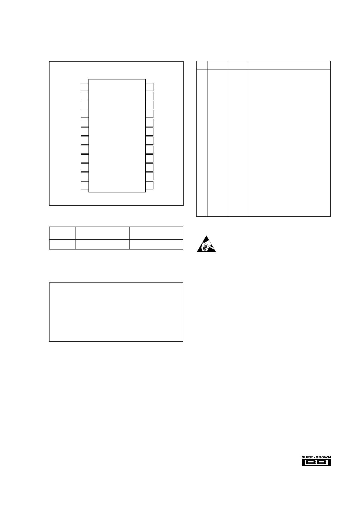
VINL
V
REF
1
REFCOM
V
REF
2
V
IN
R
RSTB
BYPAS
FMT0
FMT1
MODE0
MODE1
FSYNC
AGND
V
CC
CINPL
C
IN
NL
C
IN
PR
C
IN
NR
V
DD
DGND
SYSCLK
DOUT
BCK
LRCK
1
2
3
4
5
6
7
8
9
10
11
12
24
23
22
21
20
19
18
17
16
15
14
13
PCM1800
PIN CONFIGURATION
The information provided herein is believed to be reliable; however, BURR-BROWN assumes no responsibility for inaccuracies or omissions. BURR-BROWN assumes no
responsibility for the use of this information, and all use of such information shall be entirely at the user’s own risk. Prices and specifications are subject to change without notice.
No patent rights or licenses to any of the circuits described herein are implied or granted to any third party. BURR-BROWN does not authorize or warrant any BURR-BROWN
product for use in life support devices and/or systems.
PIN NAME I/O DESCRIPTION
1V
IN
L IN Analog Input, Lch
2V
REF
1 — Reference 1 Decoupling Capacitor
3 REFCOM — Reference Decoupling Common
4V
REF
2 — Reference 2 Decoupling Capacitor
5V
IN
R IN Input Reference, Rch
6 RSTB IN Reset Input, Active LOW
(1)
7 BYPAS IN High Pass Filter Bypass Control
(1)
8 FMT0 IN Audio Data Format 0
(1)
9 FMT1 IN Audio Data Format 1
(1)
10 MODE0 IN Master/Slave Mode Selection 0
(1)
11 MODE1 IN Master/Slave Mode Selection 1
(1)
12 FSYNC IN/OUT Frame Synchronization
13 LRCK IN/OUT Sampling Clock Input/Output (f
S
)
14 BCK IN/OUT Bit Clock Input/Output
15 DOUT OUT Audio Data Output
16 SYSCLK IN System Clock Input, 256f
S
, 384fS, or 512f
S
17 DGND — Digital Ground
18 V
DD
— Digital Power Supply
19 C
IN
NR — Anti-alias Filter Capacitor (–), Rch
20 C
IN
PR — Anti-alias Filter Capacitor (+), Rch
21 C
IN
NL — Anti-alias Filter Capacitor (–), Lch
22 C
IN
PL — Anti-alias Filter Capacitor (+), Lch
23 V
CC
— Analog Power Supply
24 AGND — Analog Ground
NOTE: (1) With 100kΩ typical pull-down resistor.
PIN ASSIGNMENTS
Top View SSOP
Supply Voltage: +V
DD, +VCC
......................................................................................
+6.5V
Supply Voltage Differences............................................................... ±0.1V
GND Voltage Differences.................................................................. ±0.1V
Digital Input Voltage ................................................. –0.3V to (V
DD
+ 0.3V)
Analog Input Voltage................................................ –0.3V to (V
CC
+ 0.3V)
Input Current (any pin except supplies) .......................................... ±10mA
Power Dissipation .......................................................................... 300mW
Operating Temperature Range ......................................... –25°C to +85°C
Storage Temperature ...................................................... –55°C to +125°C
Lead Temperature (soldering, 5s).................................................. +260°C
(reflow, 10s) ..................................................... +235°C
ABSOLUTE MAXIMUM RATINGS
PACKAGE DRAWING
PRODUCT PACKAGE NUMBER
(1)
PCM1800E 24-Pin SSOP 338
NOTE: (1) For detailed drawing and dimension table, please see end of data
sheet, or Appendix C of Burr-Brown IC Data Book.
PACKAGE INFORMATION
ELECTROSTATIC
DISCHARGE SENSITIVITY
This integrated circuit can be damaged by ESD. Burr-Brown
recommends that all integrated circuits be handled with
appropriate precautions. Failure to observe proper handling
and installation procedures can cause damage.
ESD damage can range from subtle performance degradation
to complete device failure. Precision integrated circuits may
be more susceptible to damage because very small parametric
changes could cause the device not to meet its published
specifications.
®
4
PCM1800
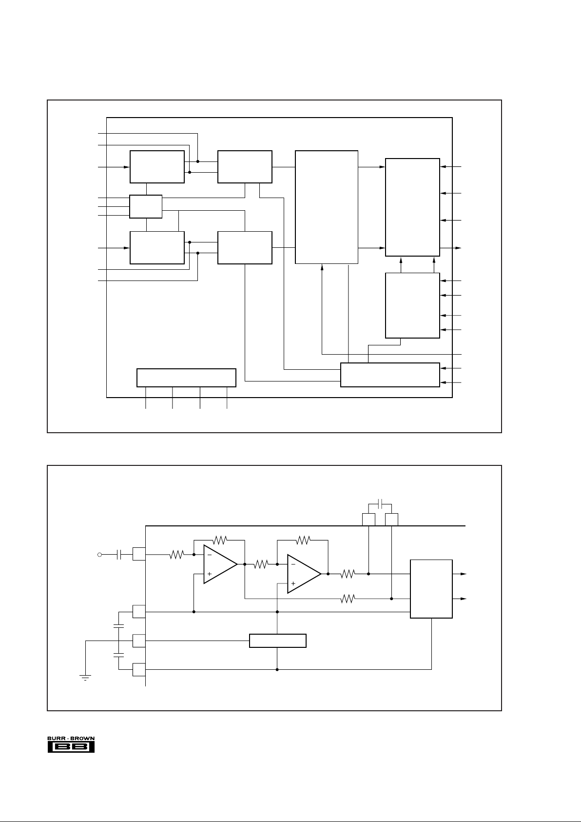
BLOCK DIAGRAM
ANALOG FRONT-END (Single-Channel)
30kΩ
1kΩ
C
EXT
470pF
2122
VINL
V
REF
2
C
IN
PL CINNL
1
4
3
2
1kΩ
Delta-Sigma
Modulator
(+)
(–)
V
REF
REFCOM
V
REF
1
+
+
1.0µF
4.7µF
+
4.7µF
Clock/Timing Control
Reset/Power Control
BYPAS
V
CC
V
DD
AGND
Reference
Mode/Format
Control
Interface
FMT0
FMT1
SYSCLK
RSTB
MODE0
MODE1
Serial Data
Interface
DOUT
BCK
LRCK
FSYNC
C
IN
PL
C
IN
NL
V
IN
L
V
REF
1
V
REF
2
V
IN
R
C
IN
NR
C
IN
PR
Power Supply
DGND
(–)
(+)
x1/64
Decimation
and
High Pass Filter
5th-Order
Delta-Sigma
Modulator
5th-Order
Delta-Sigma
Modulator
ADC
(+)
(–)
Single-End/
Differential
Converter
Single-End/
Differential
Converter
REFCOM
®
5 PCM1800
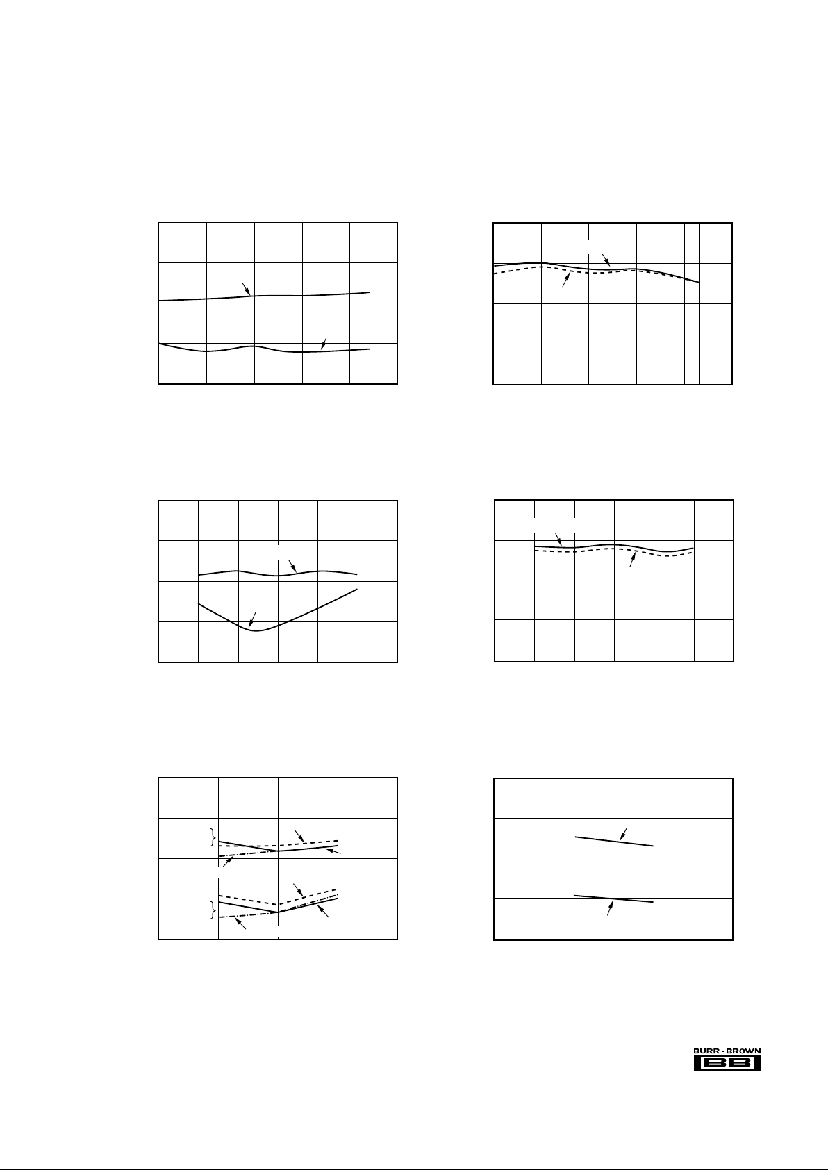
TYPICAL PERFORMANCE CURVES
At TA = +25°C, +VDD = +V
CC
= +5V, fS = 44.1kHz, and 20-bit input data, SYSCLK = 384fS, unless otherwise noted.
THD+N vs POWER SUPPLY
Supply Voltage
(V)
THD+N at –0.5dB (%)
0.010
0.008
0.006
0.004
0.002
4.5 4.75 5.0 5.25 5.5
THD+N at –60dB (%)
4.0
3.0
2.0
1.0
0
–60dB
–0.5dB
SNR and DYNAMIC RANGE vs POWER SUPPLY
Supply Voltage (V)
SNR (dB)
98
96
94
92
90
4.5 4.75 5.0 5.25 5.50
Dynamic Range (dB)
98
96
94
92
90
SNR
Dynamic Range
THD+N vs SYSTEM CLOCK
and SAMPLING FREQUENCY
System Clock
THD+N at –0.5dB (%)
0.010
0.008
0.006
0.004
0.002
256f
S
384f
S
512f
S
THD+N at –60dB (%)
4.0
3.0
2.0
1.0
0
48kHz
44.1kHz
32kHz
48kHz
32kHz
–60dB
–0.5dB
44.1kHz
THD+N vs OUTPUT DATA RESOLUTION
Resolution
THD+N at –0.5dB (%)
THD+N at –60dB (%)
0.010
0.008
0.006
0.004
0.002
16-Bit 20-Bit
4.0
3.0
2.0
1.0
0
–0.5dB
–60dB
THD+N vs TEMPERATURE
Temperature (°C)
THD+N at –0.5dB (%)
0.010
0.008
0.006
0.004
0.002
–25 0 25 50 75 85 100
THD+N at –60dB (%)
4.0
3.0
2.0
1.0
0
–60dB
–0.5dB
SNR, DYNAMIC RANGE vs TEMPERATURE
Temperature (°C)
SNR (dB)
98
96
94
92
90
–25 0 25 50 75 85 100
Dynamic Range (dB)
4.0
3.0
2.0
1.0
0
SNR
Dynamic Range
 Loading...