

Burr Brown PCM1750U, PCM1750U-1K Datasheet
1
®
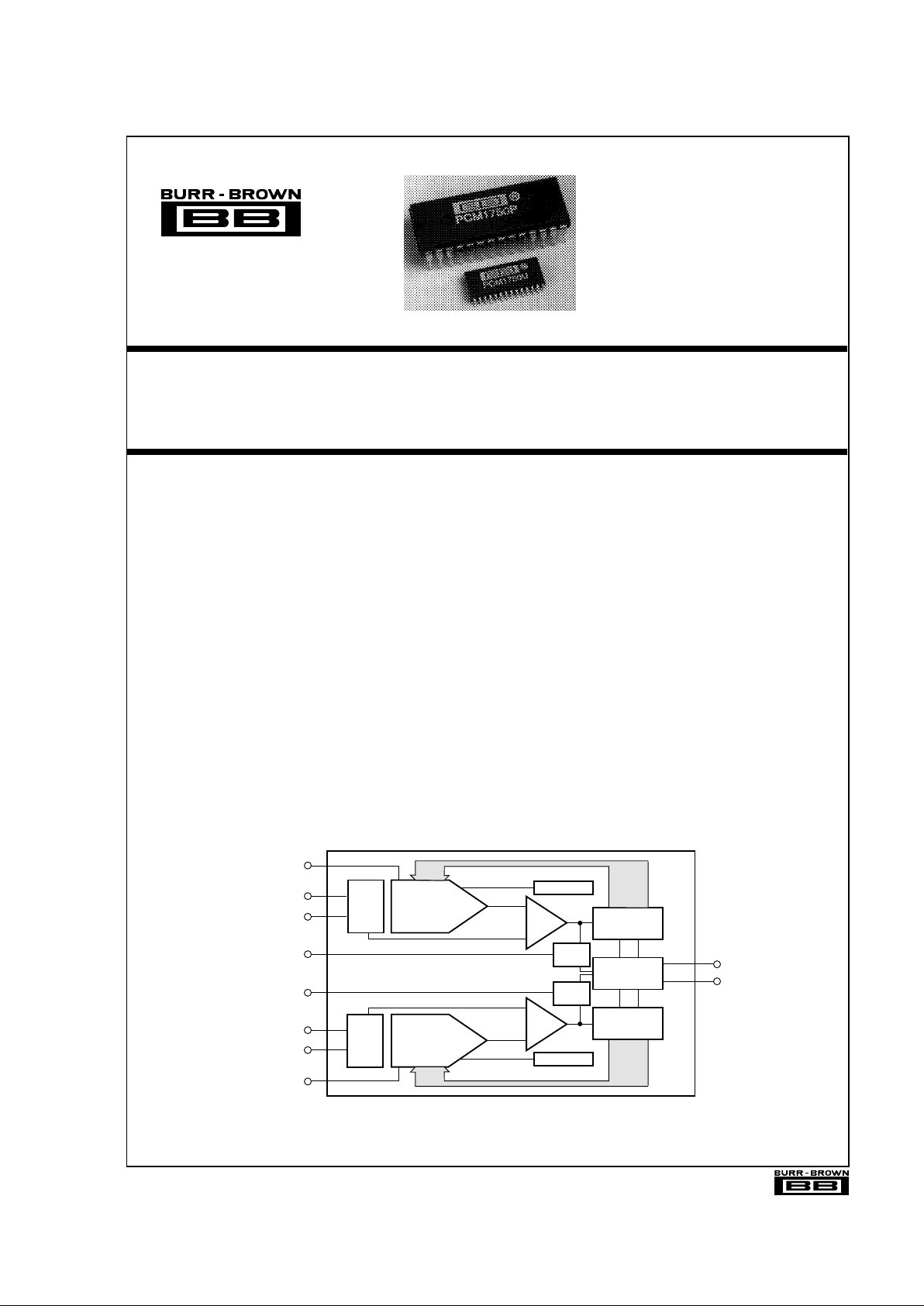
PCM1750
Dual CMOS 18-Bit Monolithic Audio
ANALOG-TO-DIGITAL CONVERTER
DESCRIPTION
The PCM1750 is a low cost, dual 18-bit CMOS
analog-to-digital converter optimized for dynamic signal applications. The PCM1750 features true co-phased
inputs with an internal sample/hold function for each
channel. The PCM1750 also comes complete with an
internal reference. Total power dissipation is less than
300mW max using ±5V voltage supplies. Low maximum Total Harmonic Distortion + Noise (–88dB max)
is 100% tested. The very fast PCM1750 is capable
of 4X x audio bandwidth oversampling rates on both
input channels simultaneously, providing greater freedom to designers in selecting input anti-aliasing filters.
PCM1750 outputs serial data in a format that is compatible with many digital filter chips and comes packaged in a space saving 28-pin plastic DIP or SOIC.
Offset Adj Right
18-Bit SAR
18-Bit SAR
CDAC
Right
S/H
CDAC
Left
S/H
Reference
V Left
S Left
S Right
Comp
Clock
Convert
Offset Adj Left
MSB Adj Right
MSB Adj Left
V Right
IN
IN
Shift Register
Control Logic
OUT
OUT
Comp
Reference
Latch
Latch
FEATURES
● DUAL 18-BIT LOW-POWER CMOS AUDIO
A/D CONVERTER
● FAST 4.5
µs MIN CONVERSION TIME
INCLUDING S/H
● VERY LOW MAX THD+N: –88dB Without
External Adjust
● COMPLETE WITH INTERNAL
REFERENCE AND DUAL S/H FUNCTION
● TWO CO-PHASE SAMPLED,
±2.75V
AUDIO INPUTS
● CAPABLE OF 4X PER CHANNEL
OVERSAMPLING RATE
● RUNS ON
±5V SUPPLIES AND
DISSIPATES 300mW MAX
● COMPACT 28-PIN PLASTIC DIP OR SOIC
International Airport Industrial Park • Mailing Address: PO Box 11400 • Tucson, AZ 85734 • Street Address: 6730 S. Tucson Blvd. • Tucson, AZ 85706
Tel: (520) 746-1111 • Twx: 910-952-1111 • Cable: BBRCORP • Telex: 066-6491 • FAX: (520) 889-1510 • Immediate Product Info: (800) 548-6132
®
PCM1750P
PCM1750U
© 1990 Burr-Brown Corporation PDS-1084B Printed in U.S.A. October, 1993
®
PCM1750 2
SPECIFICATIONS
ELECTRICAL
At 25°C, and ±VA = ±5.0V; +VD = +5.0V, unless otherwise noted. Where relevant, specifications apply to both left and right input/output channels.
NOTES: (1) Binary Two’s Complement coding. (2) The PCM1750 is tested and guaranteed at 5.2µs, however it will operate at 4.5µs. The dynamic performance is not
guaranteed or tested at this conversion rate. (3) Ratio of Signal
RMS
/ (Distortion
RMS
+ Noise
RMS
). (4) A/D converter sample frequency (4 x 48kHz; 4X oversampling per
channel). (5) A/D converter input frequency (signal level). (6) Referred to input signal level. (7) Ratio of (Distortion
RMS
+ Noise
RMS
) / Signal
RMS
. (8) Externally adjustable
to zero error. (9) Differential non-linearity error at bipolar major carry input code. Externally adjustable to zero error. (10) Full scale range (5.50V). (11) Refer to equivalent
circuit in Figure 1. (12) Worst case operating condition. Refer to typical performance curves.
PCM1750P, U
PARAMETER CONDITIONS MIN TYP MAX UNITS
RESOLUTION 18 Bits
DYNAMIC RANGE THD + N at –60dB Referred to Full Scale +88 +90 dB
ANALOG INPUT
Input Range ±2.75 V
Input Capacitance 20 pF
Aperture Delay 10 ns
Aperture Uncertainty (Jitter) 50 ps
rms
Full Power Input Bandwidth 500 kHz
DIGITAL INPUT/OUTPUT
Logic Family CMOS Compatible
Logic Level: V
IH
IIH = ±5µA +3.5 +VD + 0.3 V
V
IL
IIL = ±5µA –0.3 +1.5 V
V
OH
I
SOURCE
= 1.0mA +2.7 +4.7 V
V
OL
I
SINK
= 3.2mA +0.2 +0.4 V
Output Data Format Serial, MSB First, BTC
(1)
Convert Command Positive Edge
Convert Command Pulse Width 81 ns
Conversion Time Throughput Including Sample/Hold
(2)
4.5 5.2 20.8 µs
DYNAMIC CHARACTERISTICS (20Hz to 24kHz; 4X data decimated to 1X)
Signal-to-Noise Ratio
(3)
fs = 192kHz
(4)
; fIN = 1kHz (0dB)
(5)
+88 +90 dB
(6)
Total Harmonic Distortion + N
(7)
Without External Adjustments
f
IN
= 1kHz (0dB) fs = 192kHz –90 –88 dB
f
IN
= 1kHz (–20dB) fs = 192kHz –70 –68 dB
f
IN
= 1kHz (–60dB) fs = 192kHz –30 –28 dB
Channel Separation fs = 192kHz; f
IN
= 1kHz (0dB) and 0V +96 +108 dB
ACCURACY
Gain Error ±2 ±5%
Gain Mismatch Channel to Channel ±0.5 ±2.0 %
BPZ (Bipolar Zero) Error
(8)
±2mV
BPZ Error Mismatch Channel to Channel ±3mV
BPZ Differential Linearity Error
(9)
±0.002 % of FSR
(10)
Linearity Error ±0.003 % of FSR
Warm-up Time 1ms
DRIFT (With Internal Reference)
Gain 0°C to 70°C ±50 ppm/°C
Bipolar Zero 0°C to 70°C ±10 ppm of FSR/°C
DRIFT (Exclusive of Internal Reference)
Gain 0°C to 70°C ±10 ppm/°C
Bipolar Zero 0°C to 70°C ±3 ppm of FSR/°C
REFERENCE
V
REF
Output (Pins 19, 24):
Voltage +2.75 V
Current ±100 µA
Impedance 0.2 Ω
Accuracy ±25 mV
Drift 0°C to 70°C ±50 ppm/°C
V
REF
Input (Pins 18, P25):
Impedance
(11)
363 || 120 Ω || pF
POWER SUPPLY REJECTION % of V
IN
/ % of V
SUPPLY
(12)
0.03 % / %
POWER SUPPLY REQUIREMENTS
±V
A
Supply Voltage Range ±4.75 ±5.00 ±5.25 V
+V
D
Supply Voltage Range +4.75 +5.00 +5.25 V
+I
A
; +ID Combined Supply Current +VA; +VD = +5.0V +28 mA
–I
A
Supply Current –VA = –5.0V –13 mA
Power Dissipation ±V
A
= ±5.0V; +VD = +5.0V 210 300 mW
TEMPERATURE RANGE
Specification 0 +70 °C
Operating –40 +85 °C
Storage –60 +100 °C
3
®
PCM1750
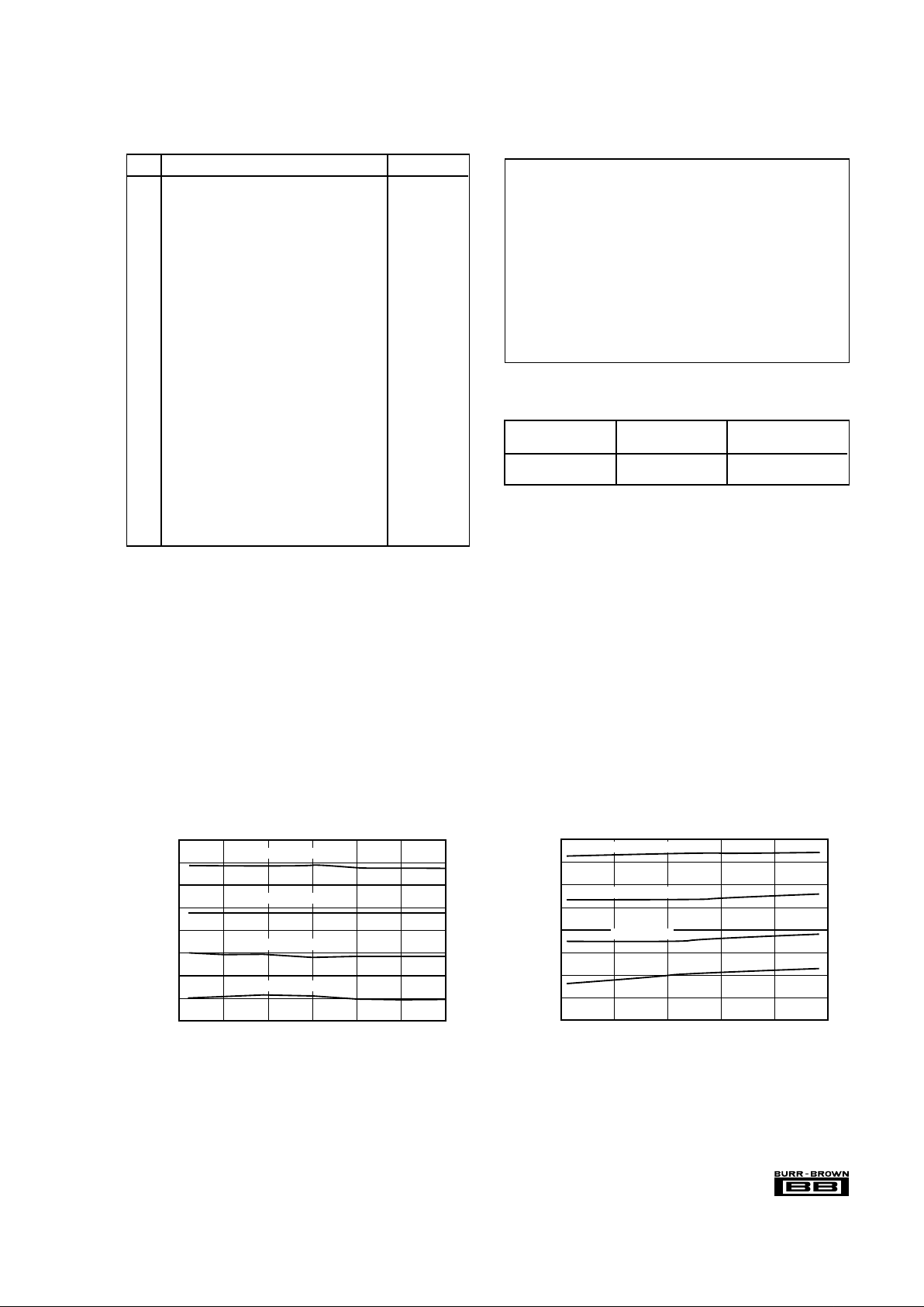
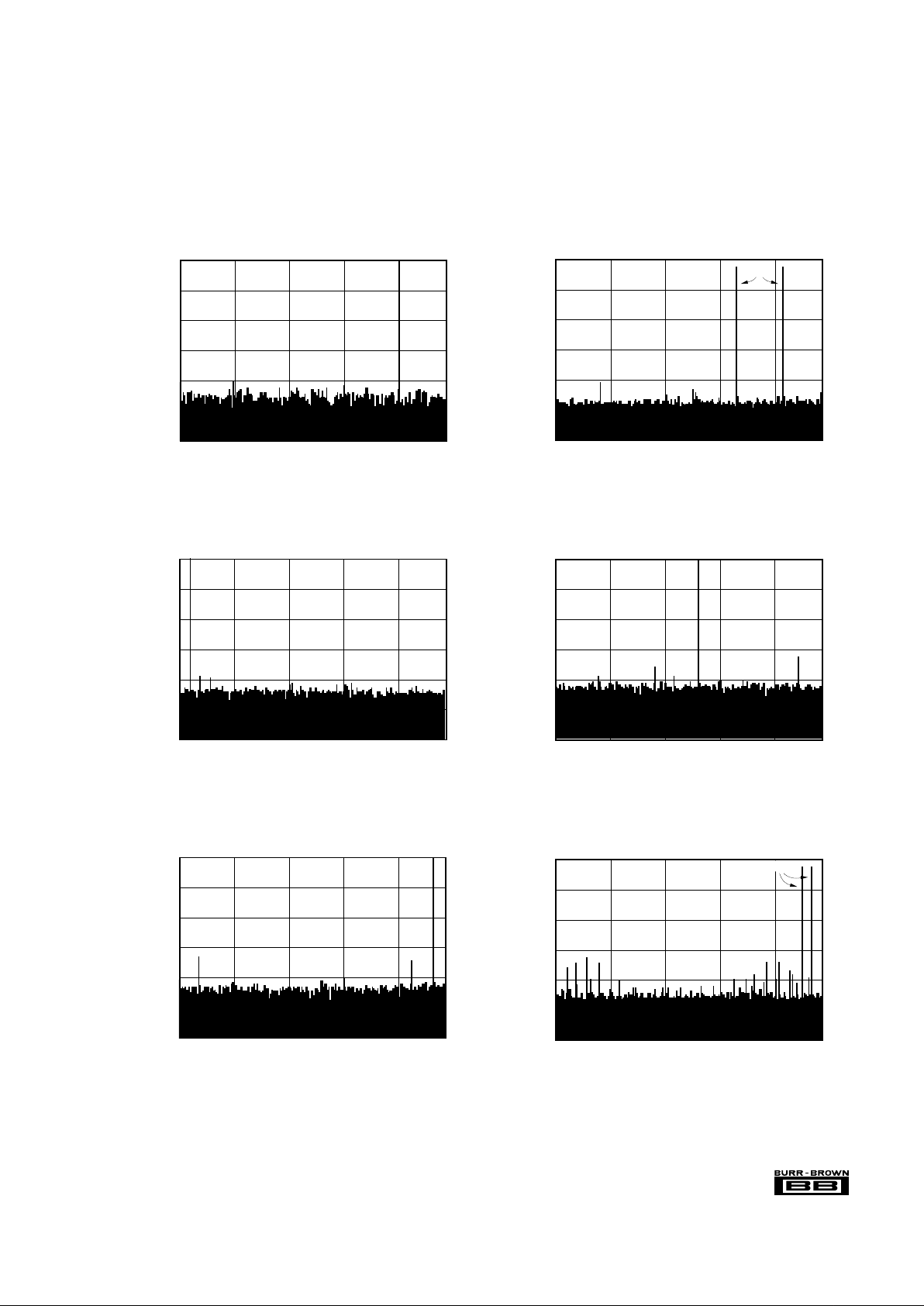
THD+N vs FREQUENCY
(Without 4X Digital Filter)
Frequency (kHz)
–20
–40
–60
–80
–100
0 20406080
100
V = –60dB
IN
V = –40dB
IN
IN
V = 0dB
IN
THD+N (dB)
V = –20dB
THD+N vs FREQUENCY
(With 4X Digital Filter)
–20
–40
–60
–80
–100
0 4 8 12 16 20 24
Frequency (kHz)
THD+N (dB)
V = –60dB
IN
V = –40dB
IN
V = –20dB
IN
V = 0dB
IN
PIN ASSIGNMENTS
PIN DESCRIPTION MNEMONIC
1 –5V Analog Supply Voltage –V
A
2 +5V Analog Supply Voltage +V
A
3 Serial Output (Left Channel) SOUTL
4 External Clock Input CLK
5 +5V Analog Supply Voltage +V
A
6 +5V Digital Voltage Supply +V
D
7 +5V Digital Voltage Supply +V
D
8 Digital Common Connection DCOM
9 Analog Common Connection ACOM
10 Digital Common Connection DCOM
11 Convert Command Input CONVERT
12 Serial Output (Right Channel) SOUTR
13 +5V Analog Supply Voltage +V
A
14 –5V Analog Supply Voltage –V
A
15 Offset Adjust (Right Channel) OFF
ADJR
16 MSB Adjust (Right Channel) MSB
ADJR
17 Analog Voltage Input (Right Channel; ±2.75V) V
INR
18 Reference Voltage Input (Right Channel) VREF
INR
19 Reference Voltage Output (Right Channel) VREF
OUTR
20 Analog Common Connection ACOM
21 Reference Voltage Decouple VREF
CAP
22 Reference Common Connection RCOM
23 Analog Common Connection ACOM
24 Reference Voltage Output (Left Channel) VREF
OUTL
25 Reference Voltage Input (Left Channel) VREF
INL
26 Analog Voltage Input (Left Channel; ±2.75V) V
INL
27 MSB Adjust (Left Channel) MSB
ADJL
28 Offset Adjust (Left Channel) OFF
ADJL
Analog Input Voltage (VIN) .................................. –VA –0.3V to +VA + 0.3V
+V
A
; +VD to ACOM/DCOM............................................................0 to +7V
–V
A
to ACOM/DCOM .................................................................... 0 to –7V
–V
A
to +VA; +VD.........................................................................0 to +14V
ACOM to DCOM .................................................................................. ±1V
Digital Inputs (pins 4, 11) to DCOM ........................... –0.3V to +V
D
+ 0.3V
Power Dissipation .......................................................................... 400mW
Lead Temperature, (soldering 10s)................................................ +300°C
Max Junction Temperature .............................................................. 165°C
Thermal Resistance,
θ
JA
: Plastic DIP............................................ 80°C/W
Thermal Resistance,
θ
JA
: Plastic SOIC .......................................100°C/W
NOTE: Stresses above those listed under Absolute Maximum Ratings may
cause permanent damage to the device. Exposure to absolute maximum
conditions for extended periods may affect device reliability.
ABSOLUTE MAXIMUM RATINGS
TYPICAL PERFORMANCE CURVES
At 25°C, and ±VA = ±5.0V; +VD = +5V, unless otherwise noted. Where relevant, specifications apply to both left and right input output channels.
PACKAGE INFORMATION
PACKAGE DRAWING
MODEL PACKAGE NUMBER
(1)
PCM1750P 28-Pin Plastic DIP 215
PCM1750U 28-Pin Plastic SOIC 217
NOTE: (1) For detailed drawing and dimension table, please see end of data
sheet, or Appendix D of Burr-Brown IC Data Book.
The information provided herein is believed to be reliable; however, BURR-BROWN assumes no responsibility for inaccuracies or omissions. BURR-BROWN assumes
no responsibility for the use of this information, and all use of such information shall be entirely at the user’s own risk. Prices and specifications are subject to change
without notice. No patent rights or licenses to any of the circuits described herein are implied or granted to any third party. BURR-BROWN does not authorize or warrant
any BURR-BROWN product for use in life support devices and/or systems.
®
PCM1750 4
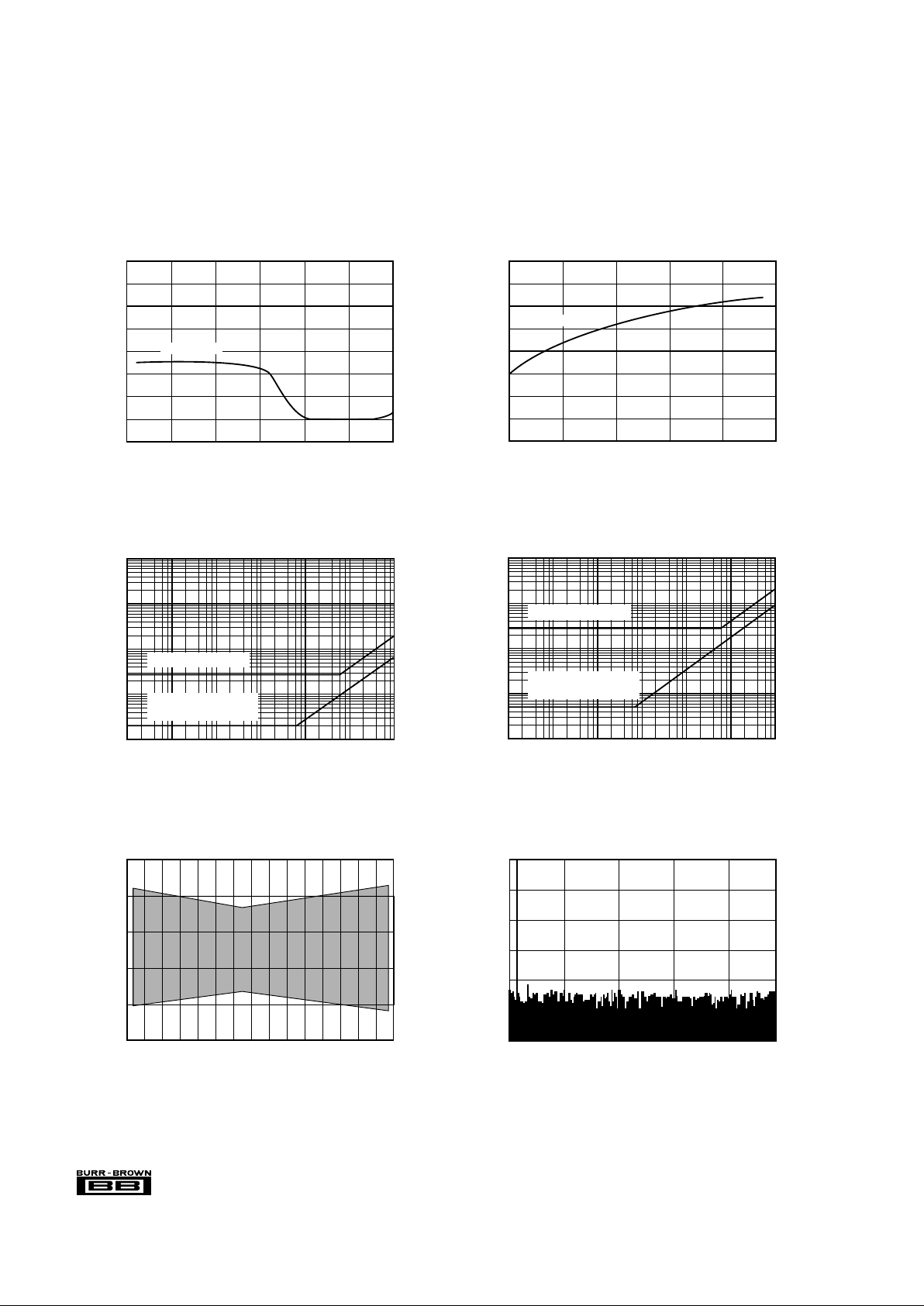
FFT 850Hz (24kHz BW; 2048 POINTS)
0
–25
–50
–75
–100
–125
–150
Amplitude (dB)
0
Frequency (kHz)
510152024
TYPICAL PERFORMANCE CURVES (CONT)
At 25°C, and ±VA = ±5.0V; +VD = +5.0V, unless otherwise noted. Where relevant, specifications apply to both left and right input-output channels.
THD vs FREQUENCY
(Without 4X Digital Filter)
Frequency (kHz)
THD (dB)
–70
–80
–90
–100
–110
0 20406080100
V = 0dB
IN
THD vs FREQUENCY
(With 4X Digital Filter)
Frequency (kHz)
–70
–80
–90
–100
–110
THD (dB)
V = 0dB
IN
0 4 8 12 16 20 24
PSR vs FREQUENCY
(–5V SUPPLY)
1
0.1
0.01
0.001
0.0001
% / %
1 10 100 1k 10k 100k 1M
Frequency (Hz)
% of V /% of V
IN SUPPLY
At BPZ:
% of FSR / % of V
SUPPLY
PSR vs FREQUENCY
(+5V SUPPLIES)
1
0.1
0.01
0.001
0.0001
% / %
1 10 100 1k 10k 100k 1M
Frequency (Hz)
% of V /% of V
IN SUPPLY
At BPZ:
% of FSR / % of V
SUPPLY
V vs TEMPERATURE
(V Outputs)
Temperature in °C
2.80
2.78
2.76
2.74
2.72
2.70
–40 –20 0 20 40 60 80 100
V
REF
(V)
REF
REF
5
®
PCM1750
FFT 88kHz and 92kHz (96kHz BW; 16384 POINTS)
0
–25
–50
–75
–100
–125
–150
Amplitude (dB)
0
Frequency (kHz)
20 40 60 80 96
–6dB
FFT 92kHz (96kHz BW; 2048 POINTS)
0
–25
–50
–75
–100
–125
–150
Amplitude (dB)
0
Frequency (kHz)
20 40 60 80 96
FFT 20kHz (24kHz BW; 2048 POINTS)
0
–25
–50
–75
–100
–125
–150
Amplitude (dB)
0
Frequency (kHz)
510152024
TYPICAL PERFORMANCE CURVES (CONT)
At 25°C, and ±VA; +VD = ±5V, unless otherwise noted. Where relevant, specifications apply to both left and right input-output channels.
FFT 17kHz and 21kHz (24kHz BW; 16384 POINTS)
0
–25
–50
–75
–100
–125
–150
Amplitude (dB)
0
Frequency (kHz)
510152024
–6dB
FFT 3.7kHz (96kHz BW; 2048 POINTS)
0
–25
–50
–75
–100
–125
–150
Amplitude (dB)
0
Frequency (kHz)
20 40 60 80 96
FFT 52kHz (96kHz BW; 2048 POINTS)
0
–25
–50
–75
–100
–125
–150
Amplitude (dB)
0
Frequency (kHz)
20 40 60 80 96
®
PCM1750 6
25k
25k
150k
5k
5k
12a
3b
3a
2b
1b
1a
2T
1T
3T
12T
off
S
C
V
REF
P16, P27
+V (+5V)
P15, P28
.01µF
P19, P24
500
13.25k
A1
A2
Latch
Comparator
Data Out
AZ
CAZ
(MSB)
S
V
C
10PF
1
2
3
IN
REF
5PF
20PF
1
L
V
S
S
3
C
2
C
1
1
CAZ
2
AZ
2
AZ
CAZ
3
3
CAZ
4
AZ
4
47k
A
.01µF
+V (+5V)
A
off
C
R
offb
500
R
12b
R
S
12T
R
R
R
S
3T
C
S
2T
C
S
1T
C
R
R
a
b
R
R
Ω
Ω
Ω
Ω
Ω
Ω
Ω
2a
R
Ω
Ω
100mV
H1 H2
P18, P25
V
Simplified
V Circuit
REFIN
REFIN
+V (+5V)
A
917
Ω
P18, P25
V
REFIN
R
offa
47k
Ω
V
REFOUT
Optional External
Adjustment Circuitry
TDAC
Auto-Zeroed Comparator
CDAC
0 to 120pF
(Code
dependent)
MSB Adj
Off Adj
= 2.75V
600
Ω
13.25k
Ω
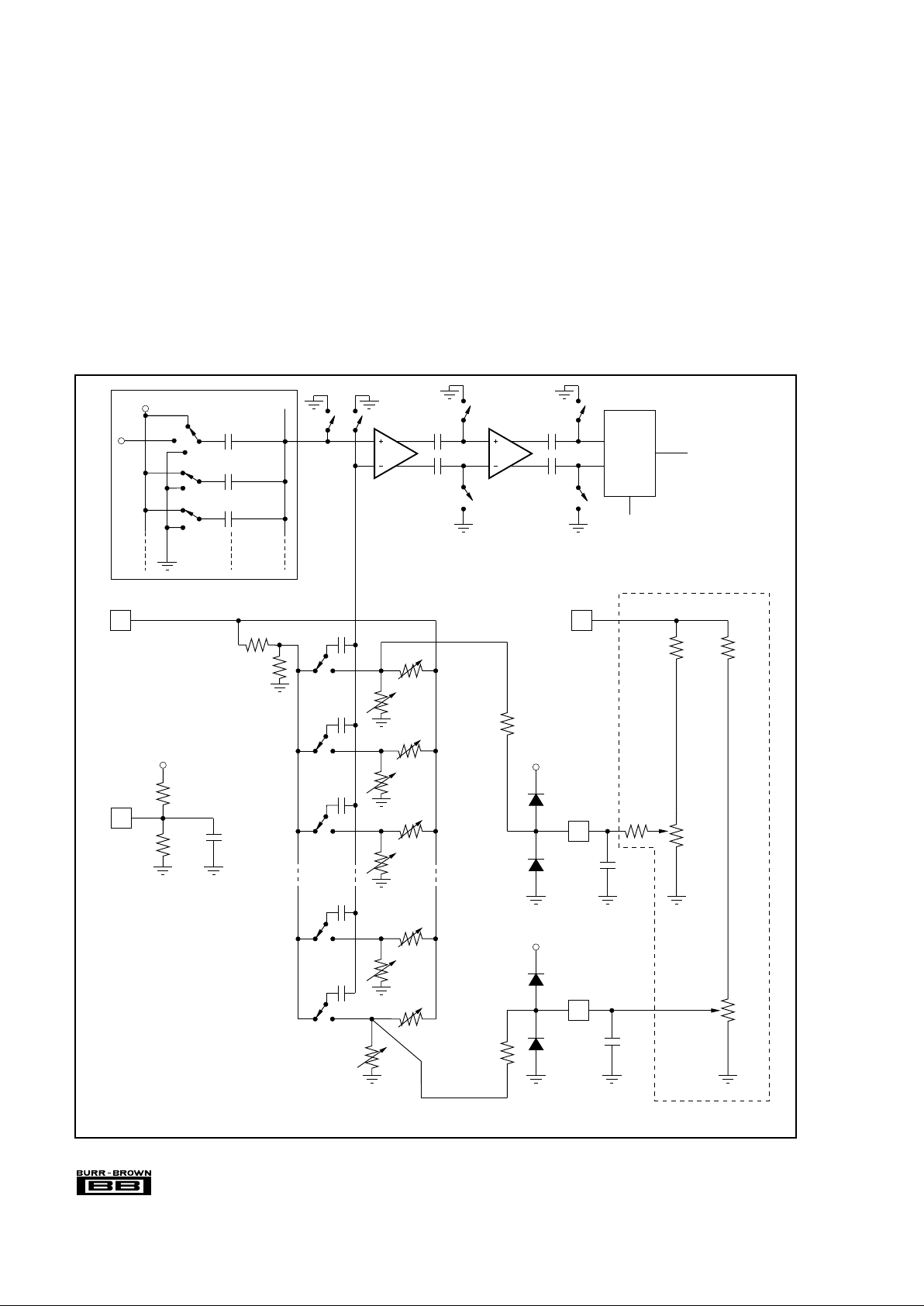
THEORY OF OPERATION
OVERVIEW
The PCM1750 is a dual 18-bit successive approximation
CMOS analog-to-digital converter with serial data outputs
designed especially for digital audio and similar applications. The single-chip converter is fabricated on a 3µ P-well
CMOS process which includes poly-poly capacitors, lasertrimmable nichrome resistors, and two layers of interconnect
metal. The dual converter employs a switched capacitor
architecture which provides separate, simultaneous S/H
(sample/hold) functions for each input channel. The separate
S/H for each channel results in a desired feature called
co-phase sampling which means that both S/H circuits are
switched at the same time into the HOLD mode to capture
their respective input signals simultaneously. This eliminates phasing errors produced by alternative architecture
ADCs which do not sample the two input channels at the
same time.
Switched binary-weighted poly-poly capacitors are used in
CDAC (capacitive digital-to-analog converter) configurations to form the successive approximation converter sec-
FIGURE 1. PCM1750 Simplified Circuit Diagram.
 Loading...